
CHAPTER 8 Defect Tolerance in VLSI Circuits
With the continuing increase in the total number of devices in VLSI circuits (e.g., microprocessors) and in the density of these devices (due to the reduction in their size) has come an increasing need for defect tolerance. Some of the millions of sub-micron devices that are included in a VLSI chip are bound to have imperfections resulting in yield-reducing manufacturing defects, where yield is defined as the percentage of operational chips out of the total number fabricated.
Consequently, increasing attention is being paid to the development and use of defect-tolerance techniques for yield enhancement, to complement existing efforts at the manufacturing stage. Design-stage yield enhancement techniques are aimed at making the integrated circuit defect tolerant, or less sensitive to manufacturing defects, and include incorporating redundancy into the design, modifying the circuit floorplan, and modifying its layout. We concentrate in this chapter on the first two, which are directly related to the focus of this book.
Adding redundant components to the circuit can help in tolerating manufacturing defects and thus increase the yield. However, too much redundancy may reduce the yield since a larger-area circuit is expected to have a larger number of defects. Moreover, the increased area of the individual chip will result in a reduction in the number of chips that can fit in a fixed-area wafer. Successful designs of defect-tolerant chips must therefore rely on accurate yield projections to determine the optimal amount of redundancy to be added. We discuss several statistical yield prediction models and their application to defect-tolerant designs. Then, various yield enhancement techniques are described and their use illustrated.
8.1 Manufacturing Defects and Circuit Faults
Manufacturing defects can be roughly classified into global defects (or gross area defects) and spot defects. Global defects are relatively large-scale defects, such as scratches from wafer mishandling, large-area defects from mask misalignment, and over- and under-etching. Spot defects are random local and small defects from materials used in the process and from environmental causes, mostly the result of undesired chemical and airborne particles deposited on the chip during the various steps of the process.
Both defect types contribute to yield loss. In mature, well-controlled fabrication lines, gross-area defects can be minimized and almost eliminated. Controlling random spot defects is considerably more difficult, and the yield loss due to spot defects is typically much greater than the yield loss due to global defects. This is especially true for large-area integrated circuits, since the frequency of global defects is almost independent of the die size, whereas the expected number of spot defects increases with the chip area. Consequently, spot defects are of greater significance when yield projection and enhancement are concerned and are therefore the focus of this chapter.
Spot defects can be divided into several types according to their location and to the potential harm they may cause. Some cause missing patterns which may result in open circuits, whereas others cause extra patterns that may result in short circuits. These defects can be further classified into intralayer and interlayer defects. Intralayer defects occur as a result of particles deposited during the lithographic processes and are also known as photolithographic defects. Examples of these are missing metal, diffusion or polysilicon, and extra metal, diffusion or polysilicon. Also included are defects in the silicon substrate, such as contamination in the deposition processes. Interlayer defects include missing material in the vias between two metal layers or between a metal layer and polysilicon, and extra material between the substrate and metal (or diffusion or polysilicon) or between two separate metal layers. These interlayer defects occur as a result of local contamination, because of, for example, dust particles.
Not all spot defects result in structural faults such as line breaks or short circuits. Whether or not a defect will cause a fault depends on its location, size, and the layout and density of the circuit (see Figure 8.1). For a defect to cause a fault, it has to be large enough to connect two disjoint conductors or to disconnect a continuous pattern. Out of the three circular missing-material defects appearing in the layout of metal conductors in Figure 8.1, the two top ones will not disconnect any conductor, whereas the bottom defect will result in an open-circuit fault.

FIGURE 8.1 The critical area for missing-metal defects of diameter x. I. Koren and Z. Koren, “Defect Tolerant VLSI Circuits: Techniques and Yield Analysis,”
Proceedings of the IEEE © 1998 IEEE.
We make, therefore, the distinction between physical defects and circuit faults. A defect is any imperfection on the wafer, but only those defects that actually affect the circuit operation are called faults: these are the only ones causing yield losses. Thus, for the purpose of yield estimation, the distribution of faults, rather than that of defects, is of interest.
Some random defects that do not cause structural faults (also termed functional faults) may still result in parametric faults; that is, the electrical parameters of some devices may be outside their desired range, affecting the performance of the circuit. For example, although a missing-material photolithographic defect may be too small to disconnect a transistor, it may still affect its performance. Parametric faults may also be the result of global defects that cause variations in process parameters. This chapter does not deal with parametric faults and concentrates instead on functional faults, against which fault-tolerance techniques can be used.
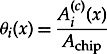
8.2 Probability of Failure and Critical Area
We next describe how the fraction of manufacturing defects that result in functional faults can be calculated. This fraction, also called the probability of failure (POF), depends on a number of factors: the type of the defect, its size (the greater the defect size, the greater the probability that it will cause a fault), its location, and circuit geometry. A commonly adopted simplifying assumption is that a defect is circular with a random diameter x (as shown in Figure 8.1). Accordingly, we denote by θi(x) the probability that a defect of type i and diameter x will cause a fault, and by θi the average POF for type i defects. Once θi(x) is calculated, θi can be obtained by averaging over all defect diameters x. Experimental data lead to the conclusion that the diameter x of a defect has a probability density function, fd(x), given by
 8.1
8.1
where
![]()
is a normalizing constant, x0 is the resolution limit of the lithography process, and xM is the maximum defect size. The values of p and xM can be determined empirically and may depend on the defect type. Typically, p ranges in value between 2 and 3.5. θican now be calculated as
![]() 8.2
8.2
Analogously, we define the critical area,
![]()
, for defects of type i and diameter x as the area in which the center of a defect of type i and diameter x must fall in order to cause a circuit failure, and by
![]()
the average over all defect diameters x of these areas.
![]()
is called the critical area for defects of type i, and can be calculated as
![]() 8.3
8.3
Assuming that given a defect, its center is uniformly distributed over the chip area, and denoting the chip area by Achip, we obtain
 8.4
8.4
and consequently, from Equations 8.2 and 8.3,
 8.5
8.5
Since the POF and the critical area are related through Equation 8.5, any one of them can be calculated first. There are several methods of calculating these parameters. Some methods are geometry based, and they calculate
![]()
first, others are Monte Carlo-type methods, where θi is calculated first.
We illustrate the geometrical method for calculating critical areas through the VLSI layout in Figure 8.1, which shows two horizontal conductors. The critical area for a missing-material defect of size x in a conductor of length L and width w is the size of the shaded area in Figure 8.1, given by
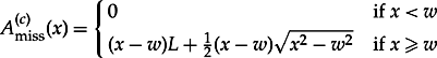 8.6
8.6
The critical area is a quadratic function of the defect diameter, but for L » w, the quadratic term becomes negligible. Thus, for long conductors we can use just the linear term. An analogous expression for
![]()
for extra-material defects in a rectangular area of width s between two adjacent conductors can be obtained by replacing w by s in Equation 8.6.
Other regular shapes can be similarly analyzed, and expressions for their critical area can be derived. Common VLSI layouts consist of many shapes in different sizes and orientations, and it is very difficult to derive the exact expression for the critical area of all but very simple and regular layouts. Therefore, other techniques have been developed, including several more efficient geometrical methods and Monte Carlo simulation methods. One geometrical method is the polygon expansion technique, in which adjacent polygons are expanded by x/2 and the intersection of the expanded polygons is the critical area for short-circuit faults of diameter x.
In the Monte Carlo approach, simulated circles representing defects of different sizes are “placed” at random locations of the layout. For each such “defect,” the circuit of the “defective” IC is extracted and compared with the defect-free circuit to determine whether the defect has resulted in a circuit fault. The POF, θi(x), is calculated for defects of type i and diameter x, as the fraction of such defects that would have resulted in a fault. It is then averaged using Equation 8.2 to produce θi, and
![]()
. An added benefit of the Monte Carlo method is that the circuit fault resulting from a given defect is precisely identified. However, the Monte Carlo approach has traditionally been very time consuming. Only recently have more efficient implementations been developed, allowing this method to be used for large ICs.
Once
![]() (or
(or ![]() )
)
has been calculated for every defect type i, it can be used as follows. Let di denote the average number of defects of type i per unit area; then the average number of manufacturing defects of type i on the chip is Achipdi. The average number on the chip of circuit faults of type i can now be expressed as
![]()
In the rest of this chapter, we will assume that the defect densities are given and the critical areas are calculated. Thus, the average number of faults on the chip, denoted by λ, can be obtained using
![]() 8.7
8.7
where the sum is taken over all possible defect types on the chip.
8.3 Basic Yield Models
To project the yield of a given chip design, we can construct an analytical probability model that describes the expected spatial distribution of manufacturing defects and, consequently, of the resulting circuit faults that eventually cause yield loss. The amount of detail needed regarding this distribution differs between chips that have some incorporated defect tolerance and those which do not. In case of a chip with no defect tolerance, its projected yield is equal to the probability of no faults occurring anywhere on the chip. Denoting by X the number of faults on the chip, the chip yield, denoted by Ychip, is given by
![]() 8.8
8.8
If the chip has some redundant components, projecting its yield requires a more intricate model that provides information regarding the distribution of faults over partial areas of the chip, as well as possible correlations among faults occurring in different subareas. In this section we describe statistical yield models for chips without redundancy; in Section 8.4, we generalize these models for predicting the effects of redundancy on the yield.
8.3.1 The Poisson and Compound Poisson Yield Models
The most common statistical yield models appearing in the literature are the Poisson model and its derivative, the Compound Poisson model. Although other models have been suggested, we will concentrate here on this family of distributions, due to the ease of calculation when using them and the documented good fit of these distributions to empirical yield data.
Let λ denote the average number of faults occurring on the chip; in other words, the expected value of the random variable X. Assuming that the chip area is divided into a very large number, n, of small statistically independent subareas, each with a probability λ/n of having a fault in it, we get the following Binomial probability for the number of faults on the chip:
Prob{X = k} = Prob{k faults occur on chip}
![]() 8.9
8.9
Letting n → ∞ Equation 8.9 results in the Poisson distribution
![]() 8.10
8.10
and the chip yield is equal to
![]() 8.11
8.11
Note that we use here the spatial (area dependent) Poisson distribution rather than the Poisson process in time discussed in Chapter 2.
It has been known since the beginning of integrated circuit manufacturing that Equation 8.11 is too pessimistic and leads to predicted chip yields that are too low when extrapolated from the yield of smaller chips or single circuits. It later became clear that the lower-predicted yield was caused by the fact that defects, and consequently faults, do not occur independently in the different regions of the chip but rather tend to cluster more than is predicted by the Poisson distribution. Figure 8.2 demonstrates how increased clustering of faults can increase the yield. The same number of faults occur in both wafers, but the wafer on the right has a higher yield due to the tighter clustering.

FIGURE 8.2 Effect of clustering on chip yield. I. Koren and Z. Koren, “Defect Tolerant VLSI Circuits: Techniques and Yield Analysis,”
Proceedings of the IEEE © 1998 IEEE.
Clustering of faults implies that the assumption that subareas on the chip are statistically independent, which led to Equation 8.9 and consequently to Equations 8.10 and 8.11, is an oversimplification. Several modifications to Equation 8.10 have been proposed to account for fault clustering. The most commonly used modification is obtained by considering the parameter λ in Equation 8.10 as a random variable rather than a constant. The resulting Compound Poisson distribution produces a distribution of faults in which the different subareas on the chip are correlated and which has a more pronounced clustering than that generated by the pure Poisson distribution.
Let us now demonstrate this compounding procedure. Let λ be the expected value of a random variable L with values ![]() and a density function fL(
and a density function fL(![]() ), where fL(
), where fL(![]() ) d
) d![]() denotes the probability that the chip fault average lies between λ and
denotes the probability that the chip fault average lies between λ and ![]() + d
+ d![]() . Averaging (or compounding) Equation 8.10 with respect to this density function results in
. Averaging (or compounding) Equation 8.10 with respect to this density function results in
![]() 8.12
8.12
and the chip yield is
![]() 8.13
8.13
The function fL(λ) in this expression is known as the compounder or mixing function. Any compounder must satisfy the conditions
![]()
The most commonly used mixing function is the Gamma density function with the two parameters λ and
![]()
![]() 8.14
8.14
![]()
(see Section 2.2). Evaluating the integral in Equation 8.12 with respect to Equation 8.14 results in the widely used Negative Binomial yield formula
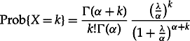 8.15
8.15
and
![]() 8.16
8.16
This last model is also called the large-area clustering Negative Binomial model. It implies that the whole chip constitutes one unit and that subareas within the same chip are correlated with regard to faults. The Negative Binomial yield model has two parameters and is therefore flexible and easy to fit to actual data. The parameter λ is the average number of faults per chip, whereas the parameter λ is a measure of the amount of fault clustering. Smaller values of λ indicate increased clustering. Actual values for λ typically range between 0.3 and 5. When λ → ∞, Expression 8.16 becomes equal to Equation 8.11, which represents the yield under the Poisson distribution, characterized by a total absence of clustering. (Note that the Poisson distribution does not guarantee that the defects will be randomly spread out: all it says is that there is no inherent clustering. Clusters of defects can still form by chance in individual instances.)
8.3.2 Variations on the Simple Yield Models
The large-area clustering compound Poisson model described above makes two crucial assumptions: the fault clusters are large compared with the size of the chip, and they are of uniform size. In some cases, it is clear from observing the defect maps of manufactured wafers that the faults can be divided into two classes—heavily clustered and less heavily clustered (see Figure 8.3)—and clearly originate from two sources: systematic and random. In these cases, a simple yield model as described above will not be able to successfully describe the fault distribution. This inadequacy will be more noticeable when attempting to evaluate the yield of chips with redundancy. One way to deal with this is to include in the model a gross yield factor Y0 that denotes the probability that the chip is not hit by a gross defect. Gross defects are usually the result of systematic processing problems that affect whole wafers or parts of wafers. They may be caused by misalignment, over- or under-etching or out-of-spec semiconductor parameters such as threshold voltage. It has been shown that even fault clusters with very high fault densities can be modeled by Y0. If the Negative Binomial yield model is used, then introducing a gross yield factor Y0 results in
FIGURE 8.3 A wafer defect map. I. Koren and Z. Koren, “Defect Tolerant VLSI Circuits: Techniques and Yield Analysis,”
Proceedings of the IEEE © 1998 IEEE.
![]() 8.17
8.17
As chips become larger, this approach becomes less practical since very few faults will hit the entire chip. Instead, two fault distributions, each with a different set of parameters, may be combined. X, the total number of faults on the chip, can be viewed as X = X1 + X2, where X1 and X2 are statistically independent random variables, denoting the number of faults of type 1 and of type 2, respectively, on the chip. The probability function of X can be derived from
 8.18
8.18
and
![]() 8.19
8.19
If X1 and X2 are modeled by a Negative Binomial distribution with parameters λ1, α1, and λ2, α2, respectively, then
![]() 8.20
8.20
Another variation on the simple fault distributions may occur in very large chips, in which the fault clusters appear to be of uniform size but are much smaller than the chip area. In this case, instead of viewing the chip as one entity for statistical purposes, it can be viewed as consisting of statistically independent regions called blocks. The number of faults in each block has a Negative Binomial distribution, and the faults within the area of the block are uniformly distributed. The large-area Negative Binomial distribution is a special case in which the whole chip constitutes one block. Another special case is the small-area Negative Binomial distribution, which describes very small independent fault clusters. Mathematically, the medium-area Negative Binomial distribution can be obtained, similarly to the large-area case, as a Compound Poisson distribution, where the integration in Equation 8.12 is performed independently over the different regions of the chip. Let the chip consist of B blocks with an average of ![]() faults. Each block will have an average of
faults. Each block will have an average of ![]() /B faults, and according to the Poisson distribution, the chip yield will be
/B faults, and according to the Poisson distribution, the chip yield will be
![]() 8.21
8.21
where
![]()
is the yield of one block.
When each factor in Equation 8.21 is compounded separately with respect to Equation 8.14, the result is
![]() 8.22
8.22
It is also possible that each region on the chip has a different sensitivity to defects, and thus, block λi has the parameters λi, αi, resulting in
 8.23
8.23
It is important to note that the differences among the various models described in this section become more noticeable when they are used to project the yield of chips with built-in redundancy.
To estimate the parameters of a yield model, the “window method” is regularly used in the industry. Wafer maps that show the location of functioning and failing chips are analyzed using overlays with grids or windows. These windows contain some adjacent chip multiples (e.g., 1, 2, and 4), and the yield for each such multiple is calculated. Values for the parameters Y0, λ, and α are then determined by means of curve fitting.
8.4 Yield Enhancement Through Redundancy
In this section we describe several techniques to incorporate redundancy in the design of VLSI circuits to increase the yield. We start by analyzing the yield enhancement due to redundancy, and then present schemes to introduce redundancy into memory and logic designs.
8.4.1 Yield Projection for Chips with Redundancy
In many integrated circuit chips, identical blocks of circuits are often replicated. In memory chips, these are blocks of memory cells, which are also known as subarrays. In digital chips they are referred to as macros. We will use the term modules to include both these designations.
In very large chips, if the whole chip is required to be fault-free, the yield will be very low. The yield can be increased by adding a few spare modules to the design and accepting those chips that have the required number of fault-free modules. However, adding redundant modules increases the chip area and reduces the number of chips that will fit into the wafer area. Consequently, a better measure for evaluating the benefit of redundancy is the effective yield, defined as
![]() 8.24
8.24
The maximum value of
![]()
determines the optimal amount of redundancy to be incorporated into the chip.
The yield of a chip with redundancy is the probability that it has enough fault-free modules for proper operation. To calculate this probability, a much more detailed statistical model than described earlier is needed, a model that specifies the fault distribution for any subarea of the chip, as well as the correlations among the different subareas of the chip.
Chips with One Type of Modules
For simplicity, let us first deal with projecting the yield of chips whose only circuitry is N identical modules, out of which R are spares and at least M = N – R must be fault-free for proper operation. Define the following probability
Fi,N = Prob{Exactly i out of the N modules are fault-free}.
Then the yield of the chip is given by
 8.25
8.25
Using the spatial Poisson distribution implies that the average number of faults per module, denoted by
![]()
. In addition, when using the Poisson model, the faults in any distinct subareas are statistically independent, and thus,
 8.26
8.26
 8.27
8.27
Unfortunately, although the Poisson distribution is mathematically convenient, it does not match actual defect and fault data. If any of the Compound Poisson distributions is to be used, then the different modules on the chip are not statistically independent but rather correlated with respect to the number of faults. A simple formula such as Equation 8.27, which uses the Binomial distribution, is therefore not appropriate. Several approaches can be followed to calculate the yield in this case, all leading to the same final expression.
The first approach applies only to the Compound Poisson models, and is based on compounding the expression in Equation 8.26 over (as shown in Section 8.3). Replacing λ/N by λ, expanding
![]()
into the binomial series
![]()
and substituting into Equation 8.26 results in
 8.28
8.28
By compounding Equation 8.28 with a density function fL(l), we obtain
Defining
![]()
(yn is the probability that a given subset of n modules is fault-free, according to the Compound Poisson model) results in
 8.29
8.29
and the yield of the chip is equal to
 8.30
8.30
The Poisson model can be obtained as a special case by substituting
![]()
whereas for the Negative Binomial model
![]() 8.31
8.31
The yield of the chip under this model is
 8.32
8.32
The approach described above to calculating the chip yield applies only to the Compound Poisson models. A more general approach involves using the Inclusion and Exclusion formula in order to calculate the probability Fi,N and results in:
 8.33
8.33
which is the same expression as in Equation 8.29 which leads to Equation 8.30.
Since Equation 8.30 can be obtained from the basic Inclusion and Exclusion formula, it is quite general and applies to a larger family of distributions than the Compound Poisson models. The only requirement for it to be applicable is that for a given n, any subset of n modules have the same probability of being fault-free, and no statistical independence among the modules is required.
As shown above, the yield for any Compound Poisson distribution (including the pure Poisson) can be obtained from Equation 8.30 by substituting the appropriate expression for yn. If a gross yield factor Y0 exists, it can be included in yn. For the model in which the defects arise from two sources and the number of faults per chip, X, can be viewed as X = X1 + X2,
![]()
where
![]()
denotes the probability that a given subset of n modules has no type j faults (j = 1, 2). The calculation of yn for the medium-size clustering Negative Binomial probability is slightly more complicated and a pointer to it is included in the Further Reading section.
More Complex Designs
The simple architecture analyzed in the preceding section is an idealization, because actual chips rarely consist entirely of identical circuit modules. The more general case is that of a chip with multiple types of modules, each with its own redundancy. In addition, all chips include support circuits which are shared by the replicated modules. The support circuitry almost never has any redundancy and, if damaged, renders the chip unusable. In what follows, expressions for the yield of chips with two different types of modules, as well as some support circuits, are presented. The extension to a larger number of module types is straightforward but cumbersome and is therefore not included.
Denote by Nj the number of type j modules, out of which Rj are spares. Each type j module occupies an area of size aj on the chip (j = 1, 2). The area of the support circuitry is ack (ck stands for chip-kill, since any fault in the support circuitry is fatal for the chip). Clearly, N1a1 + N2a2 + ack = Achip.
Since each circuit type has a different sensitivity to defects, it has a different fault density. Let λm1, λm2, and λck denote the average number of faults per type 1 module, type 2 module, and the support circuitry, respectively. Denoting by Fi1,N1,i2,N2 the probability that exactly i1 type 1 modules, exactly i2 type 2 modules, and all the support circuits are fault-free, the chip yield is given by
 8.34
8.34
where Mj = Nj – Rj (j = 1,2). According to the Poisson distribution,
 8.35
8.35
To get the expression for Fi1,N1,i2,N2 under a general fault distribution, we need to use the two-dimensional Inclusion and Exclusion formula reulting in
 8.36
8.36
where Yn1,n2 is the probability that a given set of n1 type 1 modules, a given set of n2 type 2 modules, and the support circuitry are all fault-free. This probability can be calculated using any of the models described in Section 8.3 with λ replaced by
![]()
.
Two noted special cases are the Poisson distribution, for which
![]() 8.37
8.37
and the large-area Negative Binomial distribution, for which
![]() 8.38
8.38
Some chips have a very complex redundancy scheme that does not conform to the simple M-of-N redundancy. For such chips, it is extremely difficult to develop closed-form yield expressions for any model with clustered faults. One possible solution is to use Monte Carlo simulation, in which faults are thrown at the wafer according to the underlying statistical model, and the percentage of operational chips is calculated. A much faster solution is to calculate the yield using the Poisson distribution, which is relatively easy (although complicated redundancy schemes may require some non-trivial combinatorial calculations). This yield is then compounded with respect to λ using an appropriate compounder. If the Poisson yield expression can be expanded into a power series in λ, analytical integration is possible. Otherwise, which is more likely, numerical integration has to be performed. This very powerful compounding procedure was employed to derive yield expressions for interconnection buses in VLSI chips, for partially good memory chips, and for hybrid redundancy designs of memory chips.
8.4.2 Memory Arrays with Redundancy
Defect-tolerance techniques have been successfully applied to many designs of memory arrays due to their high regularity, which greatly simplifies the task of incorporating redundancy into their design. A variety of defect-tolerance techniques have been exploited in memory designs, from the simple technique using spare rows and columns (also known as word lines and bit lines, respectively) through the use of error-correcting codes. These techniques have been successfully employed by many semiconductor manufacturers, resulting in significant yield improvements ranging from 30-fold increases in the yield of early prototypes to 1.5-fold or even 3-fold yield increases in mature processes.
The most common implementations of defect-tolerant memory arrays include redundant bit lines and word lines, as shown in Figure 8.4. The figure shows a memory array that was split into two subarrays (to avoid very long word and bit lines which may slow down the memory read and write operations) with spare rows and columns. A defective row, for example, or a row containing one or more defective memory cells can be disconnected by blowing a fusible link at the output of the corresponding decoder as shown in Figure 8.5. The disconnected row is then replaced by a spare row which has a programmable decoder with fusible links, allowing it to replace any defective row (see Figure 8.5).


The first designs that included spare rows and columns relied on laser fuses that impose a relatively large area overhead and require the use of special laser equipment to disconnect faulty lines and connect spare lines in their place. In recent years, laser fuses have been replaced by CMOS fuses, which can be programmed internally with no need for external laser equipment. Since any defect that may occur in the internal programming circuit will constitute a chip-kill defect, several memory designers have incorporated error-correcting codes into these programming circuits to increase their reliability.
To determine which rows and columns should be disconnected and replaced by spare rows and columns, respectively, we first need to identify all the faulty memory cells. The memory must be thoroughly tested, and for each faulty cell, a decision has to be made as to whether the entire row or column should be disconnected. In recent memory chip designs, the identification of faulty cells is done internally using Built-In Self-Testing (BIST), thus avoiding the need for external testing equipment. In more advanced designs, the reconfiguration of the memory array based on the results of the testing is also performed internally. Implementing self-testing of the memory is quite straightforward and involves scanning sequentially all memory locations and writing and reading 0s and 1s into all the bits. The next step of determining how to assign spare rows and columns to replace all defective rows and columns is considerably more complicated because individual defective cells can be taken care of by either replacing the cell’s row or the cell’s column. An arbitrary assignment of spare rows and columns may lead to a situation where the available spares are insufficient, while a different assignment may allow the complete repair of the memory array.
To illustrate the complexity of this assignment problem, consider the 6 × 6 memory array with two spare rows (SR0 and SR1) and two spare columns (SC0 and SC1), shown in Figure 8.6. The array has 7 of its 36 cells defective, and we need to decide which rows and columns to disconnect and replace by spares to obtain a fully operational 6 × 6 array. Suppose we use a simple Row First assignment algorithm that calls for using all the available spare rows first and then the spare columns. For the array in Figure 8.6, we will first replace rows R0 and R1 by the two spare rows and be left with four defective cells. Because only two spare columns exist, the memory array is not repaired. As we will see below, a different assignment can repair the array using the available spare rows and columns.
FIGURE 8.6 A 6 × 6 memory array with two spare rows, two spare columns, and seven defective cells (marked by x).
To devise a better algorithm for determining which rows and columns should be switched out and replaced by spares, we can use the bipartite graph shown in Figure 8.7. This graph contains two sets of vertices corresponding to the rows (R0 through R5) and columns (C0 through C5) of the memory array and has an edge connecting Ri to Cj if the cell at the intersection of row Ri and column Cj is defective. Thus, to determine the smallest number of rows and columns that must be disconnected (and replaced by spares), we need to select the smallest number of vertices in Figure 8.7 required to cover all the edges (for each edge at least one of the two incident nodes must be selected). For the simple example in Figure 8.7, it is easy to see that we should select C2 and R5 to be replaced by a spare column and row, respectively, and then select one out of C0 and R3 and, similarly, one out of C4 and R0.
FIGURE 8.7 The bipartite graph corresponding to the memory array in Figure 8.6.
This problem is known as bipartite graph edge covering and has been shown to be NP-complete. Therefore, there is currently no algorithm of polynomial complexity to solve the spare rows and columns assignment problem. We could restrict our designs to have, for example, spare rows only, which would considerably reduce the complexity of this problem. If only spare rows are available, we must replace every row with one or more defective cells by a spare row if one exists. This, however, is not a practical solution for two reasons. First, if two (or more) defects happen in a single column, we will need to use two (or more) spare rows instead of a single spare column (see for example, column C2 in Figure 8.6), which would significantly increase the required number of spare rows. Second, a reasonably common defect in memory arrays is a completely defective column (or row), which would be uncorrectable if no spare columns (or rows) are provided.
As a result, many heuristics for the assignment of spare rows and columns have been developed and implemented. These heuristics rely on the fact that it is not necessary to find the minimum number of rows and columns that should be replaced by spares, but only to find a feasible solution for repairing the array with the given number of spares.
A simple assignment algorithm consists of two steps. The first identifies which rows (and columns) must be selected for replacement. A must-repair row is a row that contains a number of defective cells that is greater than the number of currently available spare columns. Must-repair columns are defined similarly. For example, column C2 in Figure 8.6 is a must-repair column because it contains three defective cells, whereas only two spare rows are available. Once such must-repair rows and columns are replaced by spares, the number of available spares is reduced and other rows and columns may become must-repair. For example, after identifying C2 as a must-repair column and replacing it by, say SC0, we are left with a single spare column, making row R5 a must-repair row. This process is continued until no new must-repair rows and columns can be identified, yielding an array with sparse defects.
Although the first step of identifying must-repair rows and columns is reasonably simple, the second step is complicated. Fortunately, to achieve high performance, the size of memory arrays that have their own spare rows and columns is kept reasonably small (about 1 Mbit or less) and as a result, only a few defects remain to be taken care of in the second step of the algorithm. Consequently, even a very simple heuristic such as the above-mentioned row-first will work properly in most cases. In the example in Figure 8.6, after replacing the must-repair column C2 and the must-repair row R5, we will replace R0 by the remaining spare row and then replace C0 by the remaining spare column. A simple modification to the row-first algorithm that can improve its success rate is to first replace rows and columns with multiple defective cells and only then address the rows and columns which have a single defective cell.
Even the yield of memory chips that use redundant rows and columns cannot be expected to reach 100%, especially during the early phases of manufacturing when the defect density is still high. Consequently, several manufacturers package and sell partially good chips instead of discarding them. Partially good chips are chips that have some but not all of their cell arrays operational, even after using all the redundant lines.
The embedding of large memory arrays in VLSI chips is becoming very common with the most well-known example of large cache units in microprocessors. These large embedded memory arrays are designed with more aggressive design rules compared with the remaining logic units and, consequently, tend to be more prone to defects. As a result, most manufacturers of microprocessors include some form of redundancy in the cache designs, especially in the second level cache units, which normally have a larger size than the first level of caches. The incorporated redundancy can be in the form of spare rows, spare columns or spare subarrays.
Advanced Redundancy Techniques
The conventional redundancy technique (using spare rows and columns) can be enhanced, for example, by using an error-correcting code (ECC). Such an approach has been applied in the design of a 16-Mb DRAM chip. This chip includes four independent subarrays with 16 redundant bit lines and 24 redundant word lines per subarray. In addition, for every 128 data bits, nine check bits were added to allow the correction of any single-bit error within these 137 bits (this is a (137,9) SEC/DED Hamming code; see Section 3.1). To reduce the probability of two or more faulty bits in the same word (e.g., due to clustered faults), every eight adjacent bits in the subarray were assigned to eight separate words. It was found that the benefit of the combined strategy for yield enhancement was greater than the sum of the expected benefits of the two individual techniques. The reason is that the ECC technique is very effective against individual cell failures, whereas redundant rows and columns are very effective against several defective cells within the same row or column, as well as against completely defective rows and columns. As mentioned in Chapter 3, the ECC technique is commonly used in large memory systems to protect against intermittent faults occurring while the memory is in operation, in order to increase its reliability. The reliability improvement due to the use of ECC was shown to be only slightly affected by the use of the check bits to correct defective memory cells.
Increases in the size of memory chips in the last several years made it necessary to partition the memory array into several subarrays in order to decrease the current and reduce the access time by shortening the length of the bit and word lines. Using the conventional redundancy method implied that each subarray has its own spare rows and columns, leading to situations in which one subarray had an insufficient number of spare lines to handle local faults and other subarrays still had some unused spares. One obvious approach to resolve this problem is to turn some of the local redundant lines into global redundant lines, allowing for a more efficient use of the spares at the cost of higher silicon area overhead due to the larger number of required programmable fuses.
Several other approaches for more efficient redundancy schemes have been developed. One such approach was followed in the design of a 1-Gb DRAM. This design used fewer redundant lines than the traditional technique, and the redundant lines were kept local. For added defect-tolerance, each subarray of size 256 Mb (a quarter of the chip) was fabricated in such a way that it could become part of up to four different memory ICs. The resulting wafer shown in Figure 8.8 includes 112 such subarrays out of which 16 (marked by a circle in the figure) would not be fabricated in an ordinary design in which the chip boundaries are fixed.
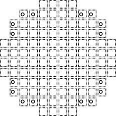
FIGURE 8.8 An 8” wafer containing 112 256-MByte subarrays. (The 16 subarrays marked with a circle would not be fabricated in an ordinary design.)
To allow this flexibility in determining the chip boundaries, the area of the subarray had to be increased by 2%, but in order to keep the overall area of the subarray identical to that in the conventional design, row redundancy was eliminated, thus compensating for this increase. Column redundancy was still implemented.
Yield analysis of the design in Figure 8.8 shows that if the faults are almost evenly distributed and the Poisson distribution can be used, there is almost no advantage in using the new design compared to the conventional design with fixed chip boundaries and use of the conventional row and column redundancy technique. There is, however, a considerable increase in yield if the medium-area Negative Binomial distribution (described in Section 8.3.2) applies. The extent of the improvement in yield is very sensitive to the fabrication parameter values.
Another approach for incorporating defect-tolerance into memory ICs combines row and column redundancy with several redundant subarrays that are to replace those subarrays hit by chip-kill faults. Such an approach was followed by the designers of another 1-Gbit memory which includes eight mats of size 128 Mbit each and eight redundant blocks of size 1 Mbit each (see Figure 8.9). The redundant block consists of four basic 256-Kbit arrays and has an additional eight spare rows and four spare columns (see Figure 8.10), the purpose of which is to increase the probability that the redundant block itself is operational and can be used for replacing a block with chip-kill faults.

FIGURE 8.9 A 1-Gb chip with eight mats of size 128 Mbit each and eight redundant blocks (RB) of size 1 Mbit each. I. Koren and Z. Koren, “Defect Tolerant VLSI Circuits: Techniques and Yield Analysis,”
Proceedings of the IEEE © 1998 IEEE.

FIGURE 8.10 A redundant block including four 256-Kbit arrays, eight redundant rows, and four redundant columns. I. Koren and Z. Koren, “Defect Tolerant VLSI Circuits: Techniques and Yield Analysis,”
Proceedings of the IEEE © 1998 IEEE.
Every mat consists of 512 basic arrays of size 256 Kbit each and has 32 spare rows and 32 spare columns. However, these are not global spares. Four spare rows are allocated to a 16-Mbit portion of the mat and eight spare columns are allocated to a 32-Mbit portion of the mat.
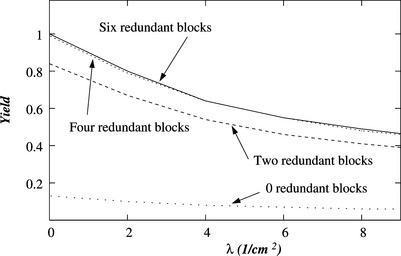
The yield of this new design of a memory chip is compared to that of the traditional design with only row and column redundancy in Figure 8.11, demonstrating the benefits of some amount of block redundancy. The increase in yield is much greater than the 2% area increase required for the redundant blocks. It can also be shown that column redundancy is still beneficial even when redundant blocks are incorporated and that the optimal number of such redundant columns is independent of the number of spare blocks.
8.4.3 Logic Integrated Circuits with Redundancy
In contrast to memory arrays, very few logic ICs have been designed with any built-in redundancy. Some regularity in the design is necessary if a low overhead for redundancy inclusion is desired. For completely irregular designs, duplication and even triplication are currently the only available redundancy techniques, and these are often impractical due to their large overhead. Regular circuits such as Programmable Logic Arrays (PLAs) and arrays of identical computing elements require less redundancy, and various defect-tolerance techniques have been proposed (and some implemented) in order to enhance their yield. These techniques, however, require extra circuits such as spare product terms (for PLAs), reconfiguration switches, and additional input lines to allow the identification of faulty product terms. Unlike memory ICs in which all defective cells can be identified by applying external test patterns, the identification of defective elements in logic ICs (even for those with regular structure) is more complex and usually requires the addition of some built-in testing aids. Thus, testability must also be a factor in choosing defect-tolerant designs for logic ICs.
The situation becomes even more complex in random logic circuits such as microprocessors. When designing such circuits, it is necessary to partition the design into separate components, preferably with each having a regular structure. Then, different redundancy schemes can be applied to the different components, including the possibility of no defect-tolerance in components for which the cost of incorporating redundancy becomes prohibitive.
We describe next two examples of such designs: a defect-tolerant microprocessor and a wafer-scale design. These demonstrate the feasibility of incorporating defect tolerance for yield enhancement in the design of processors and prove that the use of defect tolerance is not limited to the highly regular memory arrays.
The Hyeti microprocessor is a 16-bit defect-tolerant microprocessor that was designed and fabricated to demonstrate the feasibility of a high-yield defect-tolerant microprocessor. This microprocessor may be used as the core of an application-specific microprocessor-based system that is integrated on a single chip. The large silicon area consumed by such a system would most certainly result in low yield, unless some defect tolerance in the form of redundancy were incorporated into the design.
The data path of the microprocessor contains several functional units such as registers, an arithmetic and logic unit (ALU), and bus circuitry. Almost all the units in the data path have circuits that are replicated 16 times, leading to the classic bit-slice organization. This regular organization was exploited for yield enhancement by providing a spare slice that can replace a defective slice. Not all the circuits in the data path, though, consist of completely identical subcircuits. The status reg- ister, for example, has each bit associated with unique random logic and therefore has no added redundancy.
The control part has been designed as a hardwired control circuit that can be implemented using PLAs only. The regular structure of a PLA allows a straightforward incorporation of redundancy for yield enhancement through the addition of spare product terms. The design of the PLA has been modified to allow the identification of defective product terms.
Yield analysis of this microprocessor has shown that the optimal redundancy for the data path is a single 1-bit slice and the optimal redundancy for all the PLAs is one product term. A higher-than-optimal redundancy has, however, been implemented in many of these PLAs, because the floorplan of the control unit allows for the addition of a few extra product terms to the PLAs with no area penalty. A practical yield analysis should take into consideration the exact floorplan of the chip and allow the addition of a limited amount of redundancy beyond the optimal amount. Still, not all the available area should be used up for spares, since this will increase the switching area, which will, in turn, increase the chip-kill area. This greater chip-kill area can, at some point, offset the yield increase resulting from the added redundancy.
Figure 8.12 depicts the effective yield (see Equation 8.24) without redundancy in the microprocessor and with the optimal redundancy as a function of the area of the circuitry added to the microprocessor (which serves as a controller for that circuitry). The figure shows that an increase in yield of about 18% can be expected when the optimal amount of redundancy is incorporated in the design.

FIGURE 8.12 The effective yield as a function of the added area, without redundancy and with optimal redundancy, for the Negative Binomial distribution with λ = 0.05/mm2 and β = 2. I. Koren and Z. Koren, “Defect Tolerant VLSI Circuits: Techniques and Yield Analysis,”
Proceedings of the IEEE © 1998 IEEE.
A second experiment with defect-tolerance in nonmemory designs is the 3-D Computer, an example of a wafer-scale design. The 3-D Computer is a cellular array processor implemented in wafer scale integration technology. The most unique feature of its implementation is its use of stacked wafers. The basic processing element is divided into five functional units, each of which is implemented on a different wafer. Thus, each wafer contains only one type of functional unit and includes spares for yield enhancement as explained below. Units in different wafers are connected vertically through microbridges between adjacent wafers to form a complete processing element. The first working prototype of the 3-D Computer was of size 32×32. The second prototype included 128×128 processing elements.
Defect tolerance in each wafer is achieved through an interstitial redundancy scheme (see Section 4.2.3) in which the spare units are uniformly distributed in the array and are connected to the primary units with local and short interconnects. In the 32×32 prototype, a (1,1) redundancy scheme was used, and each primary unit had a separate spare unit. A (2,4) scheme was used in the 128×128 prototype; each primary unit is connected to two spare units, and each spare unit is connected to four primary units, resulting in a redundancy of 50% rather than the 100% for the (1,1) scheme. The (2,4) interstitial redundancy scheme can be implemented in a variety of ways. The exact implementation in the 3-D Computer and its effect on the yield are further discussed in the next section.
Since it is highly unlikely that a fabricated wafer will be entirely fault-free, the yield of the processor would be zero if no redundancy were included. With the implemented redundancy, the observed yield of the 32×32 array after repair was 45%. For the 128×128 array, the (1,1) redundancy scheme would have resulted in a very low yield (about 3%), due to the high probability of having faults in a primary unit and in its associated spare. The yield of the 128×128 array with the (2,4) scheme was projected to be much higher.
8.4.4 Modifying the Floorplan
The floorplan of a chip is normally not expected to have an impact on its yield. This is true for chips that are small and have a fault distribution that can be accurately described by either the Poisson or the Compound Poisson yield models with large-area clustering (in which the size of the fault clusters is larger than the size of the chip).
The situation has changed with the introduction of integrated circuits with a total area of 2 cm2 and up. Such chips usually consist of different component types, each with its own fault density, and have some incorporated redundancy. If chips with these attributes are hit by medium-sized fault clusters, then changes in the floorplan can affect their projected yield.
Consider the following example, depicted in Figure 8.13, of a chip consisting of four equal-area modules (functional units), M1, M2, M3, and M4. The chip has no incorporated redundancy, and all four modules are necessary for the proper operation of the chip.

FIGURE 8.13 Three floorplans of a 2×2 array. I. Koren and Z. Koren, “Defect Tolerant VLSI Circuits: Techniques and Yield Analysis,”
Proceedings of the IEEE © 1998 IEEE.
Assuming that the defect clusters are medium-sized relative to the chip size and that the four modules have different sensitivities to defects, we use the medium-area Negative Binomial distribution (described in Section 8.3.2) for the spatial dis- tribution of faults, with parameters λi (for module Mi) and α (per block), and
![]()
.
This chip has 4! = 24 possible floorplans. Since rotation and reflection will not affect the yield, we are left with three distinct floorplans, shown in Figure 8.13. If small-area clustering (clusters smaller than or comparable to the size of a module) or large-area clustering (clusters larger than or equal to the chip area) is assumed, the projected yields of all possible floorplans will be the same. This is not the case, however, when medium-area clustering (with horizontal or vertical blocks of two modules) is assumed.
Assuming horizontal defect blocks of size two modules, the yields of floorplans (a), (b), and (c) are
 8.39
8.39
A simple calculation shows that under the condition λ1 ≤ λ2 ≤ ;3 ≤ ;4, floorplans (a) and (b) have the higher yield. Similarly, for vertical defect blocks of size two modules,
 8.40
8.40
and floorplans (a) and (c) have the higher yield. Thus, floorplan (a) is the one which maximizes the chip yield for any cluster size. An intuitive explanation for the choice of (a) is that the less sensitive modules are placed together, increasing the chance that the chip will survive a cluster of defects.
If the previous chip is generalized to a 3 × 3 array (as depicted in Figure 8.14), and λ1 ≤ λ2 ≤ … ≤ λ9, then, unfortunately, there is no one floorplan which is always the best and the optimal floorplan depends on the cluster size. However, the following generalizations can be made.

FIGURE 8.14 Two floorplans of a 3×3 array. I. Koren and Z. Koren, “Defect Tolerant VLSI Circuits: Techniques and Yield Analysis,”
Proceedings of the IEEE © 1998 IEEE.
For all cluster sizes, the module with the highest fault density (M9) should be placed in the center of the chip, and each row or column should be rearranged so that its most sensitive module is in its center (such as, for example, floorplan (b) in Figure 8.14). Note that we reached this conclusion without assuming that the boundaries of the chip are more prone to defects than its center. The intuitive explanation to this recommendation is that placing highly sensitive modules at the chip corners increases the probability that a single fault cluster will hit two or even four adjacent chips on the wafer. This is less likely to happen if the less sensitive modules are placed at the corners.
The next example is that of a chip with redundancy. The chip consists of four modules, M1, S1, M2, and S2, where S1 is a spare for M1 and S2 is a spare for M2. The three topologically distinct floorplans for this chip are shown in Figure 8.15. Let the number of faults have a medium-area Negative Binomial distribution with an average of λ1 for M1 and S1, and λ2 for M2 and S2, and a clustering parameter of λ per block. Assuming that the defect clusters are horizontal and of size two modules each, the yields of the three floorplans are

FIGURE 8.15 Three alternative floorplans for a chip with redundancy. I. Koren and Z. Koren, “Defect Tolerant VLSI Circuits: Techniques and Yield Analysis,”
Proceedings of the IEEE © 1998 IEEE.
 8.41
8.41
 8.42
8.42
It can be easily proved that for any values of
![]()
.
If, however, the defect clusters are vertical and of size two modules, then clearly, Y(a) is given by Equation 8.42 and Y(b) = Y(c) and are given by Equation 8.41. In this case, Y(b) = Y(c) ≤ Y(a) for all values of λ1 and λ2. Floorplan (c) should therefore be preferred over floorplans (a) and (b). An intuitive justification for the choice of floorplan (c) is that it guarantees the separation between the primary modules and their spares for any size and shape of the defect clusters. This results in a higher yield, since it is less likely that the same cluster will hit both the module and its spare, thus killing the chip.
This last recommendation is exemplified by the design of the 3-D Computer, described in SubSection 8.4.3. The (2,4) structure that has been selected for implementation in the 3-D Computer is shown in Figure 8.16a.

FIGURE 8.16 The original and alternative floorplans of a wafer in the 3-D Computer. I. Koren and Z. Koren, “Defect Tolerant VLSI Circuits: Techniques and Yield Analysis,”
Proceedings of the IEEE © 1998 IEEE.
This floorplan has every spare unit adjacent to the four primary units that it can replace. This layout has short interconnection links between the spare and any primary unit that it may replace, and as a result, the performance degradation upon a failure of a primary unit is minimal. However, the close proximity of the spare and primary units results in a low yield in the presence of clustered faults, since a single fault cluster may cover a primary unit and all of its spares.
Several alternative floorplans can be designed that place the spare farther apart from the primary units connected to it (as recommended above). One such floorplan is shown in Figure 8.16b. The projected yields of the 128×128 array using the original floorplan (Figure 8.16a) or the alternative floorplan (Figure 8.16b) are shown in Figure 8.17. The yield has been calculated using the medium-area Negative Binomial distribution with a defect block size of two rows of primary units (see Figure 8.16a). Figure 8.17 clearly shows that the alternative floorplan, in which the spare unit is separated from the primary units that it can replace, has a higher projected yield.

FIGURE 8.17 The yield of the original and alternate floorplans, depicted in Figure 8.16, as a function of λ (α = 2). I. Koren and Z. Koren, “Defect Tolerant VLSI Circuits: Techniques and Yield Analysis,”
Proceedings of the IEEE © 1998 IEEE.
8.5 Further Reading
Several books (e.g., [8–10]), an edited collection of articles [5], and journal survey papers (e.g., [18,23,32,34,35,50]) have been devoted to the topic of this chapter. More specifically, for a detailed description of how critical areas and POFs can be calculated; see Chapter 5 in [10] as well as [47,53]. Two geometrical methods different from those mentioned in this chapter are the virtual artwork technique [33] and the Voronoi diagram approach [39]. Parametric faults resulting from variations in process parameters are described in [7,45].
Triangular and exponential density functions have been proposed as compounders in [36] and [42], respectively. The more commonly used (as a mixing function) Gamma distribution has been suggested in [38] and [46]. The “window method” that is used to estimate the parameters of yield models is described in [23,38,40,42,48]. It has been extended in [26] to include estimation of the block size for the medium-area clustering yield model.
Designs of defect-tolerant memories are described in [12–14,51,55,56]. The use of ECC is presented in [12]; the flexible chip boundaries scheme appears in [51] and the memory design with redundant subarrays is described in [56]. Some of these designs have been analyzed in [15,17,49]. Many techniques for assigning spare rows and columns to defective rows and columns in memory arrays have been developed, see for example [1,2,29,43]. Defect-tolerance techniques for logic circuits have been proposed (and some implemented) in [3,21,22,25,30,31,37,54, 57]. The Hyeti microprocessor is described and analyzed in [31] and the 3-D Computer is presented in [57].
The designers of many modern microprocessors have incorporated redundancy into the design of the embedded cache units. To determine the type of redundancy to be employed in the cache units of the PowerPC microprocessors, row, column, and subarray redundancies were compared considering the area and performance penalties and the expected yield improvements [52]. Based on their analysis, the designers have decided to use row only redundancy for the level-1 cache unit and row and column redundancy for the level-2 cache unit.
Intel’s Pentium Pro processor incorporates redundancy in its 512-KByte level-2 cache [11]. This cache unit consists of 72 subarrays of 64-K memory cells each, organized into four quadrants, and a single redundant subarray has been added to every quadrant. The reported increase in yield due to the added redundancy is 35%. This design includes a circuit for a BIST that identifies the faulty cells, and a flash memory circuit that is programmed to replace a defective subarray with a spare subarray.
The two 64-KBytes cache unit in Hewlett-Packard’s PA7300LC microprocessor have been designed with redundant columns. Four spare columns are included in a spare block that can be used to replace a faulty four-column block using multiplexers that are controlled by programmable fuses. A BIST circuit is included to test the cache unit and identify the faulty block [28].
The spare rows and columns assignment algorithm used in the self-repair circuit for the embedded memory unit in an Alpha microprocessor is described in [1].
The effect of floorplanning on yield has been analyzed in [16,19].
8.6 Exercises
1. Derive an expression for the critical area
![]()
(u) for square u × u missing-material defects in a conductor of length L and width w. Assume that one side of the defect is always parallel to the conductor, and that L » w so that the nonlinear edge effects can be ignored.
2. Use the polygon expansion technique to calculate approximately the critical area for circular short-circuit defects of diameter 3 for the 14×7 layout consisting of two conductors shown below:

3. Find the average critical area
![]()
for circular missing-material defects in a single conductor of length L and width w using the defect size distribution in Equation 8.1 with p = 3. Assume that L » w and ignore the nonlinear term in Equation 8.6.
4. a. Derive an expression for the critical area
![]()
of a circular missing-material defect with diameter x in the case of two conductors of length L, width w and separation s (as shown in Figure 8.1). Ignore the nonlinear terms and note that the expression differs for the three cases: x < w; w ≤ x ≤ 2w + s; and 2w + s < x ≤ xM.
![]()
using the defect size distribution in Equation 8.1 with p = 3. For simplicity, assume xM = ∞.
5. A chip with an area of 0.2 cm2 (and no redundancy) is currently manufactured. This chip has a POF of θ = 0.6 and an observed yield of Y1 = 0.87. The manufacturer plans to fabricate a similar but larger chip, with an area of 0.3 cm2, using the same wafer fabrication equipment. Assume that there is only one type of defects, and that the yield of both chips follows the Poisson model
![]()
with the same POF θ and the same defect density d.
6. A chip of area Achip (without redundancy, and with one type of defects) is currently manufactured at a yield of Y = 0.9. The manufacturer is examining the possibility of designing and fabricating two larger chips with areas of 2Achip and 4Achip. The designs and layouts of the new chips will be similar to those of the current chip (i.e., same θ), and the defect density d will remain the same.
7. For a chip without redundancy assume that X, the number of faults on the chip, follows a compound Poisson distribution.

and show that it results in the following expression for the chip yield:
![]() 8.43
8.43
b. Now use as a compounder the exponential density function
![]()
and show that it results in
![]() 8.44
8.44
c. Compare the yield expressions in Equations 8.43 and 8.44 to those for the Poisson and Negative Binomial models (for chips without redundancy) by drawing the graph of the yield as a function of λ for 0.001 ≤ λ ≤ 1.5. For the Negative Binomial model, use three values of λ, namely, λ = 0.25,2, and 5.
8. Why does the spare row in Figure 8.5 include a fusible link?
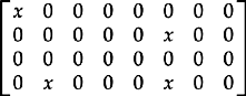
9. To a memory array with four rows and eight columns, a single spare row and two spare columns have been added. The testing of the memory array has identified four defective cells indicated by an x in the diagram below:
10. A6 × 6 memory array with two spare rows and two spare columns is shown in Figure 8.18. Show the corresponding bipartite graph, identify all the must-repair rows and columns, and select additional rows/columns to cover the remaining defective cells. Will the column-first (row-first) algorithm, if applied after replacing the must-repair rows (must-repair columns), be able to repair the memory array?
11. A chip consists of five modules, out of which four are needed for proper operation and one is a spare. Suppose the fabrication process has a fault density of 0.7 faults/cm2, and the area of each module is 0.1 cm2.

[1] Bhavsar D.K. An Algorithm for Row-Column Self-Repair of RAMs and Its Implementation in the Alpha 21264. International Test Conference (ITC’99), 1999, 311-318.
[2] Blough D. Performance Evaluation of a Reconfiguration Algorithm for Memory Arrays Containing Clustered Faults. IEEE Transactions on Reliability. June 1996;Vol. 45:274-284.
[3] Boubekeur A., Patry J.-L., Saucier G., Trilhe J. Configuring a Wafer Scale Two-Dimensional Array of Single-Bit Processors. IEEE Computer. April 1992;Vol. 25:29-39.
[4] [Special Issue on Defect, Fault, and Yield Modeling] Chiluvuri V.K.R., Koren I. Layout Synthesis Techniques for Yield Enhancement. IEEE Transactions on Semiconductor Manufacturing. May 1995;Vol. 8:178-187.
[5] Ciciani B., editor. Manufacturing Yield Evaluation of VLSI/WSI Systems. IEEE Computer Society Press, 1998.
[6] Cunningham J.A. The Use and Evaluation of Yield Models in Integrated Circuit Manufacturing. IEEE Transactions on Semiconductor Manufacturing. May 1990;Vol. 3:60-71.
[7] Director S.W., Maly W., Strojwas A.J. VLSI Design for Manufacturing: Yield Enhancement. Kluwer Academic Publishers; 1990.
[8] Ferris-Prabhu A.V. Introduction to Semiconductor Device Yield Modeling. Artech House; 1992.
[9] Gyvez J.P. Integrated Circuit Defect-Sensitivity: Theory and Computational Models. Kluwer Academic Publishers; 1993.
[10] Gyvez J.P., editor. IC Manufacturability: The Art of Process and Design Integration. IEEE Computer Society Press, 1998.
[11] [4th Quarter] Hampson C.W. Redundancy and High-Volume Manufacturing Methods. [Available at: http://developer.intel.com/technology/itj/q41997/articles/art_4.htm. Intel Technology Journal, 1997.
[12] Kalter H.L., Stapper C.H., Barth J.E., Dilorenzo J., Drake C.E., Fifield J.A., Kelley G.A., Lewis S.C., Van Der Hoeven W.B., Yankosky J.A. A 50-ns 16 Mb DRAM with 10-ns Data Rate and On-Chip ECC. IEEE Journal of Solid-State Circuits. October 1990;Vol. 25:1118-1128.
[13] Kirihata T., Watanabe Y., Wong H., DeBrosse J.K. Fault-Tolerant Designs for 256 Mb DRAM. IEEE Journal of Solid-State Circuits. April 1996;Vol. 31:558-566.
[14] Kitsukawa G., Horiguchi M., Kawajiri Y., Kawahara T. 256-Mb DRAM Circuit Technologies for File Applications. IEEE Journal of Solid-State Circuits. November 1993;Vol. 28:1105-1110.
[15] Koren I., Koren Z. Yield Analysis of a Novel Scheme for Defect-Tolerant Memories. IEEE International Conference on Innovative Systems in Silicon, October 1996, 269-278.
[16] Koren Z., Koren I. On the Effect of Floorplanning on the Yield of Large Area Integrated Circuits. IEEE Transactions on VLSI Systems, March 1997, 3-14.
[17] Koren I., Koren Z. Analysis of a Hybrid Defect-Tolerance Scheme for High-Density Memory ICs. IEEE International Symposium on Defect and Fault Tolerance in VLSI Systems, October 1997, 166-174.
[18] Koren I., Koren Z. Defect Tolerant VLSI Circuits: Techniques and Yield Analysis. Proceedings of the IEEE, Vol. 86. September 1998, 1817-1836.
[19] [Special Issue on Defect Tolerance in Digital Systems] Koren I., Koren Z. Incorporating Yield Enhancement into the Floorplanning Process. IEEE Transactions on Computers. June 2000;Vol. 49:532-541.
[20] Koren I. The Effect of Scaling on the Yield of VLSI Circuits. In: Moore W., Maly W., Strojwas A. Yield Modelling and Defect Tolerance in VLSI. Adam Hilger; 1988:91-99.
[21] Koren I., Pradhan D.K. Yield and Performance Enhancement through Redundancy in VLSI and WSI Multiprocessor Systems. Proceedings of the IEEE, Vol. 74. May 1986, 699-711.
[22] Koren I., Pradhan D.K. Modeling the Effect of Redundancy on Yield and Performance of VLSI Systems. IEEE Transactions on Computers. March 1987;Vol. 36:344-355.
[23] Koren I., Stapper C.H. Yield Models for Defect Tolerant VLSI Circuits: A Review. In: Koren I., editor. Defect and Fault Tolerance in VLSI Systems. Plenum; 1989:1-21.
[24] Koren I., Singh A.D. Fault Tolerance in VLSI Circuits. IEEE Computer, Special Issue on Fault-Tolerant Systems. July 1990;Vol. 23:73-83.
[25] Koren I., Koren Z., Pradhan D.K. Designing Interconnection Buses in VLSI and WSI for Maximum Yield and Minimum Delay. IEEE Journal of Solid-State Circuits. June 1988;Vol. 23:859-866.
[26] Koren I., Koren Z., Stapper C.H. A Unified Negative Binomial Distribution for Yield Analysis of Defect Tolerant Circuits. IEEE Transactions on Computers. June 1993;Vol. 42:724-737.
[27] Koren I., Koren Z., Stapper C.H. A Statistical Study of Defect Maps of Large Area VLSI ICs. IEEE Transactions on VLSI Systems. June 1994;Vol. 2:249-256.
[28] [Article 8] Kubicek D., Sullivan T., Mehra A., McBride J. High-Performance Processor Design Guided by System Costs. [Available at: http://www.hpl.hp.com/hpjournal/97jun/jun97a8.htm. Hewlett-Packard Journal. June 1997;Vol. 48.
[29] Kuo S.-Y., Fuchs W. Efficient Spare Allocation for Reconfigurable Arrays. IEEE Design and Test. February 1987;Vol. 4:24-31.
[30] Kuo S.-Y., Fuchs W. Kent. Fault Diagnosis and Spare Allocation for Yield Enhancement in Large Reconfigurable PLA’s. IEEE Transactions on Computers. February 1992;Vol. 41:221-226.
[31] Leveugle R., Koren Z., Koren I., Saucier G., Wehn N. The HYETI Defect Tolerant Microprocessor: A Practical Experiment and a Cost-Effectiveness Analysis. IEEE Transactions on Computers. December 1994;Vol. 43:1398-1406.
[32] Maly W. Computer-Aided Design for VLSI Circuit Manufacturability. Proceedings of IEEE, Vol. 78. February 1990, 356-392.
[33] Maly W., Moore W.R., Strojwas A. Yield Loss Mechanisms and Defect Tolerance. In: Moore W.R., Maly W., Strojwas A. Yield Modelling and Defect Tolerance in VLSI. Adam Hilger; 1988:3-30.
[34] Michalka T.L., Varshney R.C., Meindl J.D. A Discussion of Yield Modeling with Defect Clustering, Circuit Repair, and Circuit Redundancy. IEEE Transactions on Semiconductor Manufacturing. August 1990;Vol. 3:116-127.
[35] Moore W.R. A Review of Fault-Tolerant Techniques for the Enhancement of Integrated Circuit Yield. Proceedings of the IEEE, Vol. 74. May 1986, 684-698.
[36] Murphy B.T. Cost-Size Optima of Monolithic Integrated Circuits. Proceedings of the IEEE, Vol. 52. December 1964, 1537-1545.
[37] Negrini R., Sami M.G., Stefanelli R. Fault Tolerance Through Reconfiguration in VLSI and WSI arrays. MIT Press; 1989.
[38] Okabe T., Nagata M., Shimada S. Analysis of Yield of Integrated Circuits and a New Expression for the Yield. Electric Engineering Japan. December 1972;Vol. 92:135-141.
[39] Papadopoulou E. Critical Area Computation for Missing Material Defects in VLSI Circuits. IEEE Transactions on CAD. May 2001;Vol. 20:503-528.
[40] Paz O., Lawson T.R.Jr. Modification of Poisson Statistics: Modeling Defects Induced by Diffusion. IEEE Journal of Solid-State Circuits. October 1977;Vol. SC-12:540-546.
[41] Price J.E. A New Look at Yield of Integrated Circuits. Proceedings of the IEEE, Vol. 58. August 1970, 1290-1291.
[42] [Part 6] Seeds R.B. Yield, Economic, and Logistic Models for Complex Digital Arrays. IEEE International Convention Record. 1967:61-66.
[43] Sehgal A., Dubey A., Marinissen E.J., Wouters C., Vranken H., Chakrabarty K. Redundancy Modelling and Array Yield Analysis for Repairable Embedded Memories. IEE Proceedings—Computers and Digital Techniques, Vol. 152. January 2005, 97-106.
[44] Singh A.D. Interstitial Redundancy: An Area Efficient Fault Tolerance Scheme for Larger Area VLSI Processor Array. IEEE Transactions on Computers. November 1988;Vol. 37:1398-1410.
[45] Spence R., Soin R.S. Tolerance Design of Electronic Circuits. Addison-Wesley; 1988.
[46] Stapper C.H. Defect Density Distribution for LSI Yield Calculations. IEEE Transactions Electron Devices. July 1973;Vol. ED-20:655-657.
[47] Stapper C.H. Modeling of Defects in Integrated Circuit Photolithographic Patterns. IBM Journal of Research and Development. July 1984;Vol. 28:461-474.
[48] Stapper C.H. On Yield, Fault Distributions and Clustering of Particles. IBM Journal of Research and Development. May 1986;Vol. 30:326-338.
[49] Stapper C.H., McLaren A.N., Dreckmann M. Yield Model for Productivity Optimization of VLSI Memory Chips with Redundancy and Partially Good Product. IBM Journal of Research and Development. 1980;Vol. 20:398-409.
[50] Stapper C.H., Armstrong F.M., Saji K. Integrated Circuit Yield Statistics. Proceedings of the IEEE, Vol. 71. April 1983, 453-470.
[51] Sugibayashi T., Naritake I., Utsugi S., Shibahara K., Oikawa R. A 1-Gb DRAM for File Applications. IEEE Journal of Solid-State Circuits. November 1995;Vol. 30:1277-1280.
[52] Thomas T., Anthony B. Area, Performance, and Yield Implications of Redundancy in On-Chip Caches. IEEE International Conference on Computer Design, October 1999, 291-292.
[53] Walker D.M.H. Yield Simulation for Integrated Circuits. Kluwer Academic Publishers; 1987.
[54] Wey C.L. On Yield Considerations for the Design of Redundant Programmable Logic Arrays. IEEE Transactions on Computer-Aided Design. April 1988;Vol. CAD-7:528-535.
[55] Yamagata T., Sato H., Fujita K., Nishmura Y., Anami K. A Distributed Globally Replaceable Redundancy Scheme for Sub-Half-micron ULSI Memories and Beyond. IEEE Journal of Solid-State Circuits. February 1996;Vol. 31:195-201.
[56] Yoo J.-H., Kim C.-H., Lee K.-C., Kyung K.-H. A 32-Bank 1 Gb Self-Strobing Synchronous DRAM with 1 GB/s Bandwidth. IEEE Journal of Solid-State Circuits. November 1996;Vol. 31:1635-1643.
[57] Yung M.W., Little M.J., Etchells R.D., Nash J.G. Redundancy for Yield Enhancement in the 3D Computer. Wafer Scale Integration Conference, January 1989, 73-82.