
Chapter 6. Dissecting a CPU/GPU OpenCL Implementation
This chapter discusses a specific mapping of OpenCL to the combination of a Phenom II CPU and a Radeon 6970 GPU. The aim is to show how OpenCL's model maps in a specific case to give the reader some context about its execution on real hardware. We also discuss some optimizations necessary for efficient execution on such hardware.
Keywords APU, CPU, GPU, optimization, Phenom, Radeon
Introduction
In Chapter 3, we discussed trade-offs present in different architectures, many of which support the execution of OpenCL programs. The design of OpenCL is such that the model maps capably to a wide range of architectures, allowing for tuning and acceleration of kernel code. In this chapter, we discuss OpenCL's mapping to a real system in the form of a high-end AMD CPU combined with an AMD Radeon HD6970 GPU. Although AMD systems have been chosen to illustrate this mapping and implementation, each respective vendor has implemented a similar mapping for NVIDIA GPUs, Intel/ARM CPUs, and any OpenCL-compliant architecture.
OpenCL on an AMD Phenom II X6
AMD's OpenCL implementation is designed to run on both AMD GPUs and AMD's x86 CPUs in an integrated manner. All host code executes as would be expected on the general-purpose x86 CPUs in a machine, along with operating system and general application code. However, AMD's OpenCL implementation is also capable of compiling and executing OpenCL C code on x86 devices using the queuing mechanisms provided by the OpenCL runtime.
OpenCL can run on each of the six cores of an AMD Phenom II X6 chip within the larger system. Figure 6.1 shows a diagram of the AMD Phenom II X6 design.

In Figure 6.2, OpenCL is mapped onto this architecture. The entire chip is consumed by the OpenCL runtime as a single device that is obtained using clGetDeviceIDs and is passed to clCreateContext and clBuildProgram. The CPU device requires the CL_DEVICE_TYPE_CPU flag to be passed to the device types parameter of clGetDeviceIDs.
 |
| Figure 6.2 |
By treating the entire CPU as a single device, parallel workloads can be spread across the CPU cores from a single queue, efficiently using the parallelism present in the system. It is possible to split the CPU into multiple devices using the device fission extension that is discussed in a later chapter.
The OpenCL CPU runtime creates a thread to execute on each core of the CPU as a work pool to process OpenCL kernels as they are generated. These threads are passed work by a core management thread for each queue that has the role of removing the first entry from the queue and setting up work for the worker threads. Any given OpenCL kernel may comprise thousands of workgroups for which arguments must be appropriately prepared, memory allocated, and, if necessary, initialized and work queues generated.
OpenCL utilizes barriers and fences to support fine-grained synchronization. On a typical CPU-based system, in which the operating system is responsible for managing interthread communication, the cost of interacting with the operating system is a barrier to achieving efficient scaling of parallel implementations. In addition, running a single workgroup across multiple cores could create cache-sharing issues. To alleviate these issues, the OpenCL CPU runtime executes a workgroup within a single operating system thread. The OpenCL thread will run each work item in the workgroup in turn before moving onto the next work item. After all work items in the workgroup have finished executing, the worker thread will move on to the next workgroup in its work queue. As such, there is no parallelism between multiple work items within a workgroup, although between workgroups multiple operating system threads allow parallel execution when possible.
In the presence of barrier synchronization, OpenCL work items within a single workgroup execute concurrently. Each work item in the group must complete the section of the code that precedes the barrier operation, wait for other work items to reach the barrier, and then continue execution. At the barrier operation, one work item must terminate and another continue; however, it is impractical for performance reasons to let the operating system handle this with thread preemption (i.e., interrupting one thread to allow another to run). In AMD's OpenCL CPU runtime, barrier operations are supported using setjmp and longjmp. setjmp stores system state and longjmp restores it by returning to the system state at the point where setjmp was called (Gummaraju et al., 2010). In the AMD OpenCL runtime, custom versions of these two functions are provided because they need to work in cooperation with the hardware branch predictor and maintain proper program stack alignment.
An example of using a barrier in kernel foo() is shown in Figure 6.3. Note that although a CPU thread executes multiple workgroups, it will complete one workgroup at a time before moving on to the next. When a barrier is involved, it will execute every work item of that group up to the barrier, then every work item after the barrier, hence providing correct barrier semantics.
 |
| Figure 6.3 |
__kernel foo(){
…
barrier(CLK_GLOBAL_MEM_FENCE);
…
}
The AMD Phenom II microarchitecture includes 128-bit vector registers and operations from various Streaming SIMD Extension (SSE) versions. 1 OpenCL C includes a set of vector types: float2, float4, int4, and other data formats. Mathematical operations are overloaded2 on these vector types, enabling the following operations:
1SSE is a SIMD instruction set extension to the x86 architecture. Both AMD and Intel have introduced multiple generations of SSE instruction set extensions since 1999.
2Overloading is a form of polymorphism that supports reuse of the same function name over multiple parameter types, simplifying code such that only intent is required in the function name rather than intent and parameter type.
float4 a = input_data[location];
float4 b = a + (float4)(0.f, 1.f, 2.f, 3.f);
output_data[location] = b;
These vector types are stored in vector registers and operations on them compile to SSE instructions on the AMD Phenom architecture. This offers an important performance optimization. Vector load and store operations, as we also see in our low-level code discussions, improve the efficiency of memory operations. Currently, access to SSE vectors is entirely explicit within a single work item: We will see how this model differs when we discuss a GPU in the next section.
The AMD Phenom II design does not provide dedicated hardware for scratchpad memory buffers. CPUs typically provide multiple levels of memory caching in order to hide main memory access latency. The data localization provided by local memory supports efficient mapping onto the CPU cache hierarchy and allows the kernel developer to improve cache performance even in the absence of a true hardware scratchpad. To improve cache locality, local memory regions are allocated as an array per CPU thread and reused for each workgroup executed by that thread. For a sequence of workgroups, barring any data races or memory conflicts, there is then no need for this local memory to generate further cache misses and, as an additional benefit, there is no overhead from repeated calls to memory allocation routines. Figure 6.4 shows how we would map local memory to the AMD Phenom II cache.
 |
| Figure 6.4 |
Work item data stored in registers is backed into a work item stack in main memory during the setjmp call. This memory is carefully laid out to behave well in the cache, reducing cache contention and hence conflict misses and improving the utilization of the cache hierarchy. In particular, the work item stack data is staggered in memory to reduce the chance of conflicts, and data is maintained in large pages to ensure contiguous mapping to physical memory and to reduce pressure on the CPU's translation lookaside buffer. 3
OpenCL on the AMD radeon HD6970 GPU
A GPU is a significantly different target for OpenCL code compared with the CPU. The reader must remember that a graphics processor is primarily designed to render three-dimensional graphics efficiently, such that the underlying architecture is significantly different from a CPU's architecture. On current GPUs, this difference comes down to a few main features, of which the following three were discussed in Chapter 3:
• Wide single instruction multiple data (SIMD) execution: Multiple execution units execute the same instruction on different data items.
• Heavily multithreading: Support for a large number of concurrent thread contexts.
• Hardware scratchpad memory: Physical memory buffers purely under the programmer's control.
The following are additional differences that are more subtle but interesting because they create opportunities to provide improvements in terms of latency of work dispatch and communication:
Hardware synchronization support reduces the overhead of synchronizing execution of multiple thread contexts on a given SIMD core, enabling fine-grained communication at low cost.
GPUs provide extensive hardware support for task dispatch because of their deep roots in the three-dimensional graphics world. Gaming workloads involve managing complicated task graphs arising from interleaving of work in a graphics pipeline. As shown in the high-level diagram of the AMD Radeon HD6970 in Figure 3.8, the architecture consists of a command processor and group generator at the front that passes constructed groups to a pair of hardware schedulers. These two schedulers arrange compute workloads onto the 24 SIMD cores spread throughout the device. For graphics workloads, AMD includes a further set of hardware accelerator blocks below the command processor:
• Tesselator: Tessellation is the process of generating smaller triangles from larger ones to scale model complexity at runtime.
• Geometry assembler: Packages geometric information for processing by shaders.
• Rasterizer: Transforms vector data into a raster format.
• Hierarchical Z processor: Maintains a hierarchical representation of the scene depth to reduce load by providing the ability to reject pixels early based on depth.
Together, these units allow the hardware to schedule workloads as shown in Figure 6.5. To obtain the high degrees of performance acceleration associated with GPU computing, scheduling must be very efficient. Thread scheduling overhead needs to remain low because the chunks of work assembled by the input assembly may be very small—for example, a single triangle consisting of a few pixels. This amount of work alone would not keep the machine utilized, but remember that the full graphics pipeline is very quickly assembling, rasterizing and shading a large number of triangles concurrently, as shown in the schedule in Figure 6.5 (note that the unutilized compute time depicted by whitespace in the figure will fill out easily when multiple triangles are being processed concurrently). This presents a good example of why the GPU is designed for high-throughput processing and, hence, why workloads need to map properly to the underlying hardware to attain good performance.
 |
| Figure 6.5 |
In terms of OpenCL, much of this rasterization and assembly hardware is not necessary because dispatches are predefined and need only be simply assembled into work wavefronts for dispatch. However, the optimizations necessary to support this work with a deeply pipelined command processor and work generator mean that to attain good performance on a GPU of this design, we need to do the following:
• Provide a lot of work for each kernel execution
• Batch jobs together
By providing a sufficient amount of work in each kernel, we ensure that the group generation pipeline is kept occupied so that it always has more work to give to the wave schedulers and the schedulers always have more work to push onto the SIMD units. In essence, we wish to create a large number of threads to occupy the machine: As discussed previously, the GPU is a throughput machine.
The second point refers to OpenCL's queuing mechanism. When the OpenCL runtime chooses to process work in the work queue associated with the device, it scans through the tasks in the queue, selecting an appropriately large chunk to process. From this set of tasks, it constructs a command buffer of work for the GPU to process in a language understood by the command processor at the front of the GPU's pipeline. This process of (1) constructing a queue, (2) locating it somewhere in memory, (3) telling the device where it is, and (4) asking the device to process it takes time. In particular, as the GPU runs behind a driver running in kernel space, this process requires a number of context switches into and out of kernel space to allow the GPU to start running. As in the case of the CPU, where context switches between threads would become a significant overhead, switching into kernel mode and preparing queues for overly small units of work is inefficient. There is a fairly constant overhead for dispatching a work queue and further overhead for processing depending on the amount of work in it. This constant overhead must be overcome through adequate work in one or more kernels.
Threading and the Memory System
Figure 6.6 shows an approximation of the memory hierarchy of a system containing an AMD Phenom II CPU and an AMD Radeon HD6970 GPU. The CPU cache hierarchy in this setup is arranged to reduce latency of a single memory access stream: Any significant latency will cause that stream to stall and reduce execution efficiency. Because the design of the GPU cores uses threading and wide SIMD to maximize throughput at the cost of latency, the memory system is similarly designed to maximize bandwidth to satisfy that throughput, with some latency cost.
 |
| Figure 6.6 |
The limited caching associated with high-bandwidth GDDR5 on the Radeon design is made possible by the following:
• Local data shares (LDS)
• A high level of on-chip multithreading
• Coalescing through read-only and write-only caches
LDS allows for high bandwidth and low latency programmer-controlled read/write access. This form of programmable data reuse is less wasteful and also more area/power efficient than hardware-controlled caching. The reduced waste data access (data that is loaded into the cache but not used) means that the LDS can be smaller than a cache per unit area and make fewer unnecessary transfers from higher cache levels.
Hardware-controlled multithreading in the SIMD cores allows the hardware to cover latency to memory. To perform a memory access, a thread running on a SIMD unit is switched off that unit and into a separate memory controller. The thread does not resume on the SIMD until the memory access returns. To reach high levels of performance and utilization, a sufficiently large number of threads must be running. Four or 8 wavefronts (hardware thread contexts of 64 work items) per SIMD core are sufficient in many cases, although the theoretical maximum is 32 with up to eight OpenCL workgroups in flight per SIMD unit. This must be balanced against register and LDS use.
The read-only and write-only caches that are present in the system provide a filtering mechanism to combine complicated gathered read and scattered write access patterns in vector memory operations into the largest possible units. The large vector reads that often result are far more efficient for a DRAM-based system, requiring less temporal caching than the time-distributed smaller reads arising from x86 code.
The diagram in Figure 6.6 shows the PCI Express bus. All traffic between the CPU, and hence main memory, and the GPU must go through this pipe. Because PCI Express bandwidth is significantly lower than access to DRAM and even lower than the capabilities of on-chip buffers, this can become a significant bottleneck on a heavily communication-dependent application. In an OpenCL application, we need to minimize the number and size of memory copy operations relative to the kernels we enqueue. It is difficult to achieve good performance in an application that is expected to run on a discrete GPU if that application has a tight feedback loop involving copying data back and forth across the PCI Express bus.
Clause-Based SIMD Execution
The current AMD GPU architectures feature a form of decoupled execution that makes the overall design highly parallel (and, indeed, superscalar) in operation. To program such a decoupled execution, the ISA-level program forms an interesting clause-based format. In this context, a clause is a software-controlled unit of machine scheduling that divides execution into blocks with defined types for executing on distinct superscalar execution units. Having a reasonable understanding of assembly code for the GPU architecture is helpful in optimizing OpenCL code in the same way that visualizing how many SSE instructions appear in x86 assembly code can help show performance issues there. The following is a simple example of code written for the Radeon HD6970 architecture:
; -------- Disassembly --------------------
00 ALU_PUSH_BEFORE: ADDR(32) CNT(5) KCACHE0(CB0:0-15)
0x:LSHL____,R1.x,(0x00000007, 9.809089250e-45f).x
1y:ADD_INTR0.y,R0.x,PV0.x
2z:SETGT_UINT R0.z,KC0[0].y, PV1.y
3x:PREDNE_INT____,R0.z,0.0fUPDATE_EXEC_MASK UPDATE_PRED
01 JUMP POP_CNT(1) ADDR(15)
02 ALU: ADDR(37) CNT(1) KCACHE0(CB0:0-15)
4w:ADD_INTR0.w,R0.y, KC0[0].x
03 TEX: ADDR(80) CNT(1)
5VFETCH R4.x___, R0.w, fc1
FETCH_TYPE(NO_INDEX_OFFSET)
04 ALU_PUSH_BEFORE: ADDR(38) CNT(1)
6x:PREDGT____,R4.x,0.0f UPDATE_EXEC_MASK UPDATE_PRED
05 JUMPPOP_CNT(2) ADDR(15)
06 ALU:ADDR(39) CNT(2)
7z:LSHLR0.z,R0.w, 1
w:MOVR4.w,0.0f
07 TEX: ADDR(82) CNT(2)
8VFETCH R0.xy__,R0.z,fc0FORMAT(32_32_FLOAT)
FETCH_TYPE(NO_INDEX_OFFSET)
9VFETCH R1.x___,R0.w,fc2
FETCH_TYPE(NO_INDEX_OFFSET)
08 ALU: ADDR(41) CNT(3)
10x:LSHLR7.x,R0.y,(0x00000002, 2.802596929e-45f).x
w:LSHLR0.w,R0.x,(0x00000002, 2.802596929e-45f).x
09 TEX: ADDR(86) CNT(4)
11VFETCH R3.xyz_, R0.w, fc154 FORMAT(32_32_32_FLOAT)
FETCH_TYPE(NO_INDEX_OFFSET)
12VFETCH R6.xyz_, R7.x, fc154 FORMAT(32_32_32_FLOAT)
FETCH_TYPE(NO_INDEX_OFFSET)
13VFETCH R2.x___, R0.x, fc3
FETCH_TYPE(NO_INDEX_OFFSET)
14VFETCH R0.x___, R0.y, fc3
FETCH_TYPE(NO_INDEX_OFFSET)
10 ALU: ADDR(44) CNT(25) KCACHE0(CB0:0-15)
15x:ADDR5.x,-R3.x,R6.x
y:ADDR0.y,-R3.y,R6.y
z:ADDR0.z,-R3.z,R6.z
w:MOVR8.w,0.0f
16x:DOT4_e____,PV15.x,PV15.x
y:DOT4_e____,PV15.y,PV15.y
z:DOT4_e____,PV15.z,PV15.z
w:DOT4_e____,(0x80000000, -0.0f).x, 0.0f
17y:ADD____,R1.x,PV16.x
z:ADDT0.z,R1.x,-PV16.x
18x:MOVR1.x,R0.w
y:MOVR1.y,R0.w
z:MOVR1.z,R0.w
w:MUL_e____,R4.x,PV17.y
19x:RCP_e____,PV18.w
y:RCP_e____,PV18.w
z:RCP_e____,PV18.w
20z:MUL_e____,T0.z,PV19.x
21y:MUL_e____,KC0[0].z,PV20.z
22x:MUL_e____,R2.x,PV21.y
w:MUL_eR0.w,R0.x, PV21.yVEC_120
23x:MULADD_eR4.x,-R5.x, PV22.x, R3.x
y:MULADD_eR4.y,-R0.y,PV22.x, R3.y
z:MULADD_eR4.z,-R0.z,PV22.x,R3.z
11 MEM_RAT_CACHELESS_STORE_DWORD__NI: RAT(0)[R1], R4, ARRAY_SIZE(4)
MARK VPM
12 ALU: ADDR(69) CNT(6)
24x:MULADD_eR8.x,R5.x,R0.w, R6.x
y:MULADD_eR8.y,R0.y,R0.w, R6.y
z:MULADD_eR8.z,R0.z,R0.w,R6.z
25x:MOVR7.x,R7.x
y:MOVR7.y,R7.x
z:MOVR7.z,R7.x
13 MEM_RAT_CACHELESS_STORE_DWORD__NI: RAT(0)[R7], R8, ARRAY_SIZE(4)
MARK VPM
14 POP (2) ADDR(15)
15 NOP NO_BARRIER
16 END
END_OF_PROGRAM
The leftmost code at 00, 01, 02, and so on at the leftmost indentation level is a control flow program. This code executes on the wave scheduler unit, interleaved between any of the wavefronts running on that scheduler's half of the device. This program, and hence the scheduler, handles all branching and mask management, using values returned from ALU workloads. The latency of executing each control flow instruction is relatively high, on the order of 40 or more cycles between executing one clause from a given wavefront and executing the next. This latency is easily covered if the code contains a lot of ALU work and there are enough wavefronts to execute while the first is returning to the scheduler for control flow execution. A glance at the ISA code gives some idea of how efficiently it will schedule if combined with enough wavefronts.
Lines 02, 04, etc. are ALU operations within the control flow program. These statements initiate ALU clauses. At these points, the scheduler passes control to one of the SIMD units whereby that SIMD unit will process the ALU operations within the clause. Once an ALU clause starts on a SIMD engine, it runs to completion, with no more control flow occurring internally. Note two important features of these ALU clauses, although only the first is directly apparent in the code:
• This is a single-lane instruction stream; that is, they are not wide SIMD instructions.
• The clauses contain VLIW instructions, visible as x, y, z, w entries.
The idea of programming a SIMD architecture using a lanewise model was discussed previously. In this case, the ISA code seen here is just one kernel instance representing exactly what we would see in the OpenCL kernel that generated it. The SIMD engine executes 64-wide logical SIMD entities called wavefronts. Each wavefront utilizes a single instruction decode and has its own instruction stream and can be viewed as a separate hardware thread context. The 64 work items within the wavefront execute over four clock cycles over a 16-lane hardware SIMD unit. Different wavefronts execute at different points in their instruction streams. All branching is performed at this wavefront granularity. Any sub-wavefront branching will require replaying of the clauses within the wave scheduler until all combinations have correctly executed and hence this divergence creates inefficiency. The same issues arise when developing for competing architectures such as NVIDIA's GTX580 design and are inherent in software production for wide vector architectures, whether manually vectorized or hardware vectorized as are these architectures.
A diagram of the SIMD unit that executes this code is shown in Figure 6.7. Each SIMD unit contains a 32-ported LDS with a four-operation latency and atomic units on its interface. These atomic units mean that non-returning atomic operations can be executing on the LDS at the same time as ALU operations executing within the ALUs, offering further parallelism. Colliding reads or writes to LDS are replayed over multiple cycles until the operation is complete. For reads, this can cause the ALUs to stall.
 |
| Figure 6.7 |
The VLIW packets that the architecture can execute are very flexible, running through four near-identical ALUs, as can be seen in Figure 6.8. Each way of the VLIW unit can execute full 32-bit floating point operations, 24-bit integer operations (using the floating point mantissa), and 32-bit integer adds. These operations need not be identical, as is apparent in packet 15 in the code, in which three floating point addition operations and a single move execute in the same VLIW packet. VLIW ways can combine resources in various combinations to execute a wider range of double precision and integer operations with fewer than four per packet. For example, one double precision floating point multiply can be executed per cycle, giving double precision multiplication a 4:1 slowdown compared with single precision multiplication.

VLIW execution leads to a high level of efficiency from the architecture where a significant ALU capacity requires little control logic to go with it. However, the necessity for the compiler to extract VLIW packets leads to a significant reduction in efficiency in most cases, and in the code example we can see that only four ALU packets are completely full of operations. Where a VLIW packet executes with fewer than four slots filled, the hardware is wasting possible execution resources. The compiler is fairly good at extracting VLIW packets from code if there are no dependencies, and as a result, unrolled loops or, even better, vectorization of code allow for the best utilization because they provide the compiler with as many independent instructions as possible. In this way, we see that unlike the AMD CPU implementation of OpenCL that was entirely explicitly vectorized, the code for the AMD Radeon HD6970 architecture is both implicit and explicit. It is implicit in that it programs a vector architecture lanewise, relying on hardware vectorization to map the individual work items represented by the ISA code to hardware. It is explicit because small-scale source vectorization assists filling VLIW packets, maximizing memory bandwidth and utilizing the per-lane vector register file.
Line 07 initiates a texture clause. Within a texture clause, memory read operations execute within the texture fetch hardware. This execution is independent of ALU work executing on the SIMD unit and hence a memory operation can be executing from one wavefront while an ALU operation is executing on another.
Resource Allocation
Each SIMD unit on the GPU includes a fixed amount of register and LDS storage space. There are 256 kB of registers on each SIMD unit, available as 256 128-bit vector registers for each work item across a 64-element wavefront. These registers will be divided based on the number of wavefronts executing on the SIMD unit. There are 32 kB of LDS on each SIMD unit, accessible as a random access 32-bank SRAM with two ports per work item for read and write. The LDS is divided between the number of workgroups executing on the SIMD unit, based on the local memory allocation requests made within the kernel and through the OpenCL runtime parameter-passing mechanism.
When executing a single kernel on each SIMD unit, as is the standard mapping when running an OpenCL program, we might see a resource bottleneck, as seen in Figure 6.9. In this diagram, we see two workgroups each containing two wavefronts, where each work item (and hence wavefront scaled up) needs 42 registers and the workgroup needs 12 kB of LDS. This allocation of four wavefronts per SIMD is limited by the LDS requirements of the workgroup and is near the minimum number of wavefronts we need to run on the device to hide memory latency. The minimum number of wavefronts to cover instruction latency and utilize the SIMD unit is three—two in ALU clauses in the two instruction slots on the SIMD unit and one performing memory accesses. In realistic conditions, three is insufficient due to control flow. If we can increase the number of wavefronts running on the SIMD unit to six or more, we have a better chance of hiding control flow and, particularly, memory latency, where the more threads running, the better our latency hiding. Because we are LDS limited in this case, increasing the number of wavefronts per workgroup to three would be a good start if this is practical for the algorithm. Alternatively, reducing the LDS allocation would allow us to run a third workgroup on each core, which is very useful if one wavefront is waiting on barriers or memory accesses and hence not on the SIMD unit at the time.
 |
| Figure 6.9 |
Each workgroup runs on a single SIMD core and stays on that core until completion. The reason for this should be clear when seeing the amount of state storage required by that group: In this case, we see 12 kB of LDS and 84 kB of registers per workgroup. This would be a significant amount of data to have to flush to memory and move to another core. As a result, when control flow code is executing in the wave scheduler, if there is not another wavefront with ALU work to perform ready to be scheduled onto the SIMD unit, hardware will lie idle.
Memory performance considerations in OpenCL
OpenCL Global Memory
Issues related to memory in terms of temporal and spatial locality were discussed in Chapter 3. Obtaining peak performance from an OpenCL program depends heavily on utilizing memory efficiently. Unfortunately, efficient memory access is highly dependent on the particular device on which the OpenCL program is running. Access patterns that may be efficient on the GPU may be inefficient when run on a CPU. Even when we move an OpenCL program to GPUs from different manufacturers, we can see substantial differences. However, there are common practices that will produce code that performs well across multiple devices.
In all cases, a useful way to start analyzing memory performance is to judge what level of throughput a kernel is achieving. A simple way to do this is to calculate the memory bandwidth of the kernel:
EB is the effective bandwidth;
Br is the number of bytes read from global memory;
Bw is the number of bytes written to global memory; and
T is the time required to run the kernel.
T can be measured using profiling tools such as the AMD Stream Profiler (which is discussed in Chapter 11). Br and Bw can often be calculated by multiplying the number of bytes each work item reads or writes by the global number of work items. Of course, in some cases, this number must be estimated because we may branch in a data-dependent manner around reads and writes.
Once we know the bandwidth measurement, we can compare it with the peak bandwidth of the execution device and determine how far away we are from peak performance: The closer to peak, the more efficiently we are using the memory system. If our numbers are far from peak, then we can consider restructuring the memory access pattern to improve utilization.
Spatial locality is an important consideration for OpenCL memory access. Most architectures on which OpenCL runs are vector based at some level (whether SSE-like vector instructions or lanewise programmed hardware-vectorized such as AMD IL or NVIDIA PTX), and their memory systems benefit from issuing accesses together across this vector. In addition, localized accesses offer caching benefits.
On most modern CPUs, there is a vector instruction set; the various versions of SSE and the AVX are good examples. For efficient memory access, we want to design code such that full, aligned, vector reads are possible using these instruction sets. Given the small vector size, the most efficient way to perform such vector reads is to give the compiler as much information as possible by using vector data types such as float4. Such accesses make good use of cache lines, moving data between the cache and registers as efficiently as possible. However, on these CPUs, caching helps cover some of the performance loss from performing smaller, unaligned, or more randomly addressed reads. Figures 6.10 and 6.11 provide a simple example of the difference between a single contiguous read and a set of four random reads. Not only do the narrower reads hit multiple cache lines (creating more cache misses if they do not hit in the cache) but they also cause less efficient transfers to be passed through the memory system.
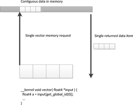 |
| Figure 6.10 |
 |
| Figure 6.11 If we transfer the same four floats as in Figure 6.10 but with a more random pattern, we return smaller chunks of memory through the memory system less efficiently. |
GPU memory architectures differ significantly from CPU memory architectures, as discussed in Chapter 3. GPUs use multithreading to cover some level of memory latency and are biased in favor of ALU capability rather than caching and sophisticated out-of-order logic. Given the large amounts of compute resources available on typical GPUs, it becomes increasingly important to provide high bandwidth to the memory system if we do not want to starve the GPU. Many modern GPU architectures, particularly high-performance desktop versions such as the latest AMD Radeon and NVIDIA GeForce designs, utilize a wide-SIMD architecture. Imagine the loss of efficiency in Figure 6.11 scaled to a 64-wide hardware vector, as we see in the AMD Radeon HD6970 architecture.
Efficient access patterns differ even among these architectures. For an x86 CPU with SSE, we would want to use 128-bit float4 accesses, and we would want as many accesses as possible to fall within cache lines to reduce the number of cache misses. For the AMD Radeon HD6970 GPU architecture, 16 consecutive work items will issue a memory request at the same time. These requests will be delayed in the memory system if they cannot be efficiently serviced. For peak efficiency, each of these 16 should issue a 128-bit read such that the reads form a contiguous 256-byte memory region so that the memory system can create a single large memory request. To achieve reasonable portability across different architectures, a good general solution is to compact the memory accesses as effectively as possible, allowing the wide vector machines (AMD and NVIDIA GPUs) and the narrow vector machines (x86 CPUs) to both use the memory system as efficiently as possible. To achieve this, we should access memory across a whole workgroup starting with a base address aligned to workgroupSize * loadSize, where loadSize is the load issued per work item, and which should be reasonably sized—preferably 128 bits on x86 CPUs and AMD GPU architectures and expanding to 256 bits on AVX-supported architectures.
Further complications arise when dealing with the specifics of different memory systems, such as reducing conflicts on the off-chip links to DRAM. For example, let us consider the way in which the AMD Radeon HD6970 architecture allocates its addresses. Figure 6.12 shows that the low 8 bits of the address are used to select the byte within the memory bank; this gives us the cache line and sub-cache line read locality. If we try to read a column of data from a two-dimensional array, we already know that we are inefficiently using the on-chip buses. It also means that we want multiple groups running on the device simultaneously to access different memory channels and banks. Each memory channel is an on-chip memory controller corresponding to a link to an off-chip memory (Figure 6.13). We want accesses across the device to be spread across as many banks and channels in the memory system as possible, maximizing concurrent data access. However, a vector memory access from a single wavefront that hits multiple memory channels (or banks) occupies those channels, blocking access from other wavefronts and reducing overall memory throughput. Optimally, we want a given wavefront to be contained with a given channel and bank, allowing multiple wavefronts to access multiple channels in parallel. This will allow data to stream in and out of memory efficiently.
| Figure 6.12 |
 |
| Figure 6.13 |
To avoid using multiple channels, a single wavefront should access addresses from within a 64-word region, which is achievable if all work items read 32 bits from consecutive addresses. The worst possible situation is if each work item in multiple wavefronts reads an address with the same value above bit 8: Each one hits the same channel and bank, and accesses are serialized, achieving a small fraction of peak bandwidth. More details on this subject for AMD architectures can be found in AMD's OpenCL programming guide (Advanced Micro Devices, Incorporated, 2011). Similar information is provided to cover the differences in competing architectures from the respective vendors—for example, NVIDIA's CUDA programming guide (NVIDIA Corporation, 2010).
Local Memory as a Software-Managed Cache
Most OpenCL-supporting devices have some form of cache support. Due to their graphics-oriented designs, many GPUs have read-only data caches that enable some amount of spatial reuse of data.
The easiest way to guarantee this use on the widest range of devices is to use Images (discussed in Chapter 5). Images map data sets to the texture read hardware and, assuming that complicated filtering and two-dimensional access modes are not needed, improve memory efficiency on the GPU. However, GPU caches are small compared with the number of active thread contexts reading data. Programmer-controlled scratchpad memory in the local address space is an efficient approach for caching read data with less overhead from wasted space than hardware-controlled caches, better power efficiency, and higher performance for a given area. It is also useful as a way to exchange data with other work items in the same workgroup with a very low and, more important, guaranteed access latency.
The code in Figure 5.11 shows a simple example of this approach. The code loads a range of data from A into C and then accesses multiple values from it, avoiding a second read from DRAM. At the same time, the code loads a single value from aLocalArray just once and reuses it across all work items in the group, thereby considerably reducing the memory traffic. In some CPU hardware implementations, some of this reuse occurs in the cache, whereas sometimes all of it occurs in the cache (especially on x86 processors). Given that we have knowledge of the underlying memory access patterns, we can control how much reuse of data is present in the application.
Of course, there are trade-offs when considering how best to optimize data locality. In some cases, the overhead of the extra copy instructions required to move data into local memory and then back out into the ALU (possibly via registers) will sometimes be less efficient than simply reusing the data out of cache. Moving data into local memory is most useful when there are large numbers of reads and writes reusing the same locations, when the lifetime of a write is very long with a vast number of reads using it, or when manual cache blocking offers a way to correct for conflict misses that can often be problematic in two-dimensional data access patterns.
In the case of read/write operations, the benefit of local memory becomes even more obvious, particularly given the wide range of architectures with read-only caches. Consider, for example, the following relatively naive version of a prefix sum code:
void localPrefixSum(
__local unsigned *prefixSums,
unsigned numElements ) {
// Run through levels of tree halving sizes of the element set
// performing reduction phase
int offset = 1;
for( int level = numElements/2; level > 0; level /= 2 ) {
barrier(CLK_LOCAL_MEM_FENCE);
for( int sumElement = get_local_id(0);
sumElement < level;
sumElement += get_local_size(0) ) {
int ai = offset*(2*sumElement+1)-1;
int bi = offset*(2*sumElement+2)-1;
prefixSums[bi] = prefixSums[ai] + prefixSums[bi];
}
offset *= 2;
}
barrier(CLK_LOCAL_MEM_FENCE);
// Need to clear the last element
if( get_local_id(0) == 0 ) {
prefixSums[ numElements-1 ] = 0;
}
// Push values back down the tree
for( int level = 1; level < numElements; level *= 2 ) {
offset /= 2;
barrier(CLK_LOCAL_MEM_FENCE);
for( int sumElement = get_local_id(0);
sumElement < level;
sumElement += get_local_size(0) ) {
int ai = offset*(2*sumElement+1)-1;
int bi = offset*(2*sumElement+2)-1;
unsigned temporary = prefixSums[ai];
prefixSums[ai] = prefixSums[bi];
prefixSums[bi] = temporary + prefixSums[bi];
}
}
}
Although the previous code is not optimal for many architectures, it does effectively share data between work items using a local array. The data flow of the first loop (level = numElements>>1 to 0) is shown in Figure 6.14. Note that each iteration of the loop updates a range of values that a different work item will need to use on the next iteration. Note also that the number of work items collaborating on the calculation decreases on each iteration. The inner loop masks excess work items off to avoid diverging execution across the barrier. To accommodate such behavior, we insert barrier operations to ensure synchronization between the work items and so that we can guarantee that the data will be ready for the execution of the next iteration.
 |
| Figure 6.14 |
The prefix sum code discussed previously uses local memory in a manner that is inefficient on most wide SIMD architectures, such as high-end GPUs. As mentioned in the discussion on global memory, memory systems tend to be banked to allow a large number of access ports without requiring multiple ports at every memory location. As a result, scratchpad memory hardware (and caches, similarly) tends to be built such that each bank can perform multiple reads or concurrent reads and writes (or some other multiaccess configuration), whereas multiple reads will be spread over multiple banks. This is an important consideration when we are using wide SIMD hardware to access memory. An AMD GPU can issue four instructions, including up to two load instructions simultaneously through the VLIW unit in each of the 16 SIMD lanes on a given clock cycle. As a result, it performs as many as 32 reads or writes from the local memory buffer (LDS) on a single cycle when local memory instructions are issued in a VLIW packet. If each bank supports a single access port, then we can only achieve this throughput if all accesses target different memory banks because each bank can only provide one value. On this architecture, because each work item can perform two reads or writes per cycle, the local data share is constructed of 32 banks. Similar rules arise on competing architectures; NVIDIA's Fermi architecture, for example, also has a 32-banked local memory.
The problem for local memory is not as acute as that for global memory. In global memory, we saw that widely spread accesses would incur latency because they might cause multiple cache line misses. In local memory, at least on architectures with true scratchpads, the programmer knows when the data is present because he or she put it there manually. The only requirement is that the 16 accesses we issue as part of that read or write instruction hit different banks.
Figure 6.15 shows a simplification for comparison—step 2 of the prefix sum in Figure 6.14 accessing a local memory with eight memory banks, where each work item can perform a single local memory operation per cycle. In this case, our local memory buffer can return up to eight values per cycle from memory. What result do we obtain when performing the set of accesses necessary for step 1 of the prefix sum?
 |
| Figure 6.15 Step 1 of Figure 6.14 showing behavior with a local memory of eight banks and one access per work item per cycle. |
Note that our 16-element local memory (necessary for the prefix sum) is spread over two rows. Each column is a bank, and each row is an address within a bank. Assuming (as is common in many architectures) that each bank is 32 bits wide, our memory address would break down as shown at the top of Figure 6.15. Two consecutive memory words will reside in separate banks. As with global memory, a SIMD vector that accesses consecutive addresses along its length will efficiently access the local memory banks without contention. In Figure 6.15, however, we see a different behavior. Given the second access to local memory, the read from prefixSums[bi] in
prefixSums[bi] = prefixSums[ai] + prefixSums[bi];
tries to read values from locations 3, 7, 11, and 15. As shown in Figure 6.15, 3 and 11 both sit in bank 3; 7 and 15 both sit in bank 7. There is no possible way to read two rows from the same bank simultaneously, so these accesses will be serialized on GPUs by the hardware, incurring a read delay. For good performance, we might wish to restructure our code to avoid this conflict. One useful technique is to add padding to the addresses, and an example of this is shown in Figure 6.16. By shifting addresses after the first set (aligning to banks), we can change evenly strided accesses to avoid conflicts. Unfortunately, this adds address computation overhead, which can be more severe than the bank conflict overhead; hence, this trade-off is an example of architecture-specific tuning.
 |
| Figure 6.16 Figure 6.15 with padding added in the data structures showing how it removes the conflict in this case. |
Local memory should be carefully rationed. Any device that uses a real scratchpad region that is not hardware managed will have a limited amount of local memory. In the case of the AMD Radeon HD6970 GPU, this space is 32 kB, following OpenCL minimum requirements. It is important to note that this 32 kB is shared between all workgroups executing simultaneously on the core. Also, because the GPU is a latency hiding throughput device that utilizes multithreading on each core, the more workgroups that can fit, the better the hardware utilization is likely to be. If each workgroup uses 16 kB, then only two can fit on the core. If these workgroups contain a small number of wavefronts (one or two), then there will only barely be enough hardware threads to cover latency. Therefore, local memory allocation will be needed to balance efficiency gains from sharing and efficiency losses from reducing the number of hardware threads to one or two on a multithreaded device.
The OpenCL API includes calls to query the amount of local memory the device uses, and this can be used to parameterize kernels before the programmer compiles or dispatches them. The first call in the following code queries the type of the local memory so that it is possible to determine if it is dedicated or in global memory (which may or may not be cached; this can also be queried), and the second call returns the size of each local memory buffer:
cl_int err;
cl_device_local_mem_type type;
err = clGetDeviceInfo(
deviceId,
CL_DEVICE_LOCAL_MEM_TYPE,
sizeof(cl_device_local_mem_type),
&type,
0 );
cl_ulong size;
err = clGetDeviceInfo(
deviceId,
CL_DEVICE_LOCAL_MEM_SIZE,
sizeof( cl_ulong ),
&size,
0 );
Summary
The aim of this chapter was to show a very specific mapping of OpenCL to an architectural implementation. In this case, it was shown how OpenCL maps slightly differently to a CPU architecture and a GPU architecture. The core principles of this chapter apply to competing CPU and GPU architectures, but significant differences in performance can easily arise from variation in vector width (32 on NVIDA GPUs, 32/64 on AMD GPUs, and much smaller on CPUs), variations in thread context management, and instruction scheduling. It is clear that in one book we cannot aim to cover all possible architectures, but by giving one example, it is hoped that further investigation through vendor documentation can lead to efficient code on whatever OpenCL device is being targeted.
References
Advanced Micro Devices, Incorporated, The AMD Accelerated Parallel Processing—OpenCL Programming Guide. (2011) Advanced Micro Devices, Inc, Sunnyvale, CA.
Association for Computing Machinery, PACT ′10: Proceedings of the Nineteenth International Conference on Parallel Architectures and Compilation Techniques: September 11–15, 2010, Vienna, Austria. (2010) Association for Computing Machinery.
Gummaraju, J.; Morichetti, L.; Houston, M.; Sander, B.; Gaster, B.R.; Zheng, B., Twin Peaks: A Software Platform for Heterogeneous Computing on General-Purpose and Graphics Processors. (2010) Association for Computing Machinery, New York.
NVIDIA Corporation, NVIDIA CUDA C Programming Guide. (2010) NVIDIA Corporation, Santa Clara, CA.
..................Content has been hidden....................
You can't read the all page of ebook, please click here login for view all page.