
12
Nonlinear All‐Optical Switch
Rajarshi Dhar1, Arpan Deyasi2, and Angsuman Sarkar3
1 Department of Electronics and Telecommunication Engineering, IIEST, Shibpur, Howrah, West Bengal, India
2 Department of Electronics and Communication Engineering, RCC Institute of Information Technology, Kolkata, West Bengal, India
3 Department of Electronics and Communication Engineering, Kalyani Government Engineering College, Kalyani, West Bengal, India
12.1 Introduction
The limitations of electrical communication systems have led people to move to optical communication systems. The optical communication systems have proven to be much more advantageous over the electrical systems as they overcome the problems or limitations like bandwidth, speed, security, reduced system noise, and several other factors which are undesirable for a faithful and sustainable communication system [1, 2]. But one of the problems in optical systems is that of optical processing. The optical processors that have been developed until now can only process low‐speed signals or signals with low bit rates. The processors need electrical signals which are converted from optical signals are processed and then converted back to optical signals. This is done using the Optical‐Electrical‐Optical Switches or OEO Switches [3, 4]. Now this conversion and back‐conversion takes up a lot of power and time which are not desirable for high‐speed systems. Thus this leads to the need for all‐optical processing systems, which include the all‐optical switches.
12.2 Classification of All‐Optical Switches
There are several types of all‐optical switches, namely thermo‐optical switches, acousto‐optical switches, liquid crystal optical switches, and nonlinear optical switches.
12.2.1 Thermo‐Optical Switch
There are several types of all‐optical switches, including thermo‐optical switches [5–7]. The operation of thermo‐optical switches is based upon the principle of thermal effects on optical properties [8]. The thermo‐optic effect is a basic property which is available in all optical materials. The thermo‐optic coefficient or TOC given by dε/dT is the fundamental parameter which depicts how the refractive index depends on temperature, where ε is the complex dielectric function of the material at temperature T. The TOC is a very important factor for applications of optics and optoelectronics. The several applications include light guidance, coupling of light and radiation modulation. It is very much important and necessary to obtain a theoretically correct result, i.e. its absolute magnitude and its sign, over a wide range of frequencies, based on the little available values at a few frequencies. A number of thermo‐optical switches have been developed over the years. They include interferometric devices, such as Mach–Zender IF, directional coupler, and optical digital switches.
For all isotropic materials in the transparent regime, the macroscopic Clausius–Mossotti formula is applicable:
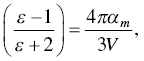
where αm is the polarizability of a bulk small sphere (measured in macroscopic scale) with a volume V which is much larger when compared with the lattice dimensions. The numbers of effects which are responsible for the temperature dependence of dielectric constant are three in total. They are: direct volume expansion effect, dependence of polarizability on volume expansion, and dependence of polarizability on temperature.
Differentiating Equation 12.1 with respect to temperature one gets

where the terms given by A, B and C represent the following:
- A: With increase in temperature, the volume increases and thus the inter‐atomic spaces increase too which causes a decrease of dielectric constant. This is direct effect of volume expansion.
- B: Increase of polarizability with the volume expansion.
- C: Temperature dependence of polarizability at constant volume.
The temperature derivative of volume can be called the linear thermal expansion coefficient, given by
Thus Equation 12.2 can be written as

Thus this is the equation that governs the working of the thermal‐optical switches. The permittivity of the material is related to the RI of the material by e=n2. Thus by putting e=√n in the above equations, one can easily get the temperature dependence of the RI to temperature.
12.2.2 Acousto‐Optic Switch
The second type of all‐optical switch is the acousto‐optic switch. These work on the principle of the elasto‐optic effect. This is the occurrence of periodic modulations within the RI of the material when a sound or acoustic wave moves through the transparent medium. This provides a grating which has a moving phase which causes some portion of the incident light to move in different directions [9]. This phenomenon which is known as the acousto‐optic diffraction, conceptually utilized to manifest various optical devices that can be used to perform space‐domain, time‐domain, and frequency‐domain modulations of electromagnetic spectrum [10]. These devices find extensive applications in optoelectronic systems starting from controlling of light beam to signal and data processing applications to wavelength routing [11, 12].
The theory for acousto‐optic switches is given in [9]. As mentioned above, the elasto‐optic effect is the most important mechanism for acousto‐optic operation. To describe the effect in crystals Pockels gave the phenomenological theory which helps in the introduction of elasto‐optic tensor. Deformation gradient is a symmetric term defined when wave is propagated in elastic medium

where ui is the displacement. Six independent components of symmetric strain sensor are defined in following way:
- odd scattering parameters:
(12.6.1)

- even scattering parameters:
(12.6.2)

The conventional elasto‐optic effect that was introduced by Pockel said that the impermeability tensor ∆Bij is directly proportional to strain tensor in linear fashion
where pijkl is the elasto‐optic tensor. If it is written in contracted notation one gets
In modern research, however, the conventional theory has been changed and the elasto‐optic effect introduced. This is basically the nonlinear polarization which arises owing to the modulation of dielectric tensor ∆εij. Since εij and Bij are inversely proportional to each other in a principal axis system, hence
where ni is the refractive index. Replacing Equation 12.7 into Equation 12.9, we can write
where the elasto‐optic susceptibility tensor i
There are two other modifications of the elasto‐optic effect, namely the roto‐optic effect and the indirect elasto‐optic effect.
The roto‐effect was introduced by Nelson and Lax [13], where they found that the elasto‐optic effect is not originated from the classical concept of working principle of birefringent crystals and described that due to the anti‐symmetric part of the deformation gradient, there exists an additional roto‐optic susceptibility given by
where Rij = (Sij − Sji)/2.
The indirect‐optic effect arises in piezoelectric crystals as a result of the piezoelectric effect succeeded by the elasto‐optic effect. Thus the original elasto‐optic tensor changes and the effective elasto‐optic tensor is given by [14]

where pij is the direct elasto‐optic tensor, rim is the electro‐optic tensor, ejn is the piezoelectric tensor, εmn is dielectric tensor, and Sm is unit acoustic wave vector.
12.2.3 Liquid Crystal Optical Switch
It is the third type of all‐optical switch. Refractive index and absorption are the two most important and practical parameters of a liquid crystal mixture or compound. All the light modulation mechanisms are dependent on the change in refractive indices. The absorption coefficient has a very important crucial effect on the photostability. The electronic structure of the crystals determines the refractive indices and absorption property of the crystal in the visible spectral region. Now the physical mechanisms that are used for modulating light are described briefly in the next part:
- Dynamic Scattering: When a nematic liquid crystal is subjected to a DC or low‐frequency AC field [15], electro‐hydrodynamic flow is induced by the conductivity anisotropy ionic motion. Through viscous friction, electro‐hydrodynamic flow is connected with alignment at molecular level. This makes liquid crystal in turbulent mode results in strong scattering of light. Large electric field of 104 V/cm is required to produce such effect. The contrast ratio of minimum‐to‐maximum intensities is around 1:20 and the response time is 200 ms.
- Guest‐Host Effect: These systems are produced by dissolving 1–5% of dichroic dye in a liquid crystal [16]. The substrate material should be unclouded enough in the spectrum of the desired area. It is important for the dichroic molecules to have weak absorption for one polarization and strong absorption for the other in order to obtain higher contrast ratio. To obtain high absorption in the field‐off state, molecules of the dye are closely aligned to the polarization of the incident wave. Absorption can be reduced when directors of liquid crystal [17] are re‐oriented by the field, and consequent re‐orientation of dye molecules. The guest‐host effects in ferroelectric liquid crystals are published in various literatures.
- Field‐induced Nematic‐cholesteric Phase Change: This mechanism has been observed experimentally [18, 19]. The liquid crystal at the initial stage is at the cholesteric phase where it attains the same structure as a helical one and has its axis aligned to the substrate (made by glass). As a result, incident light suffers from scattering and therefore a whitish layer appears on the glass substrate. The nematic phase is observed in the helix when applied bias exceeds 105 V/cm. In the nematic condition, alignment is seen in the helix. The result is that that cell becomes transparent.
- Field‐induced Director Axis Re‐orientation: This is a common example of electro‐optic effect on aligned nematic and ferroelectric liquid crystal for light modulation. Different methods have already been applied for perfect alignment of nematic crystals, and some are reported as very successful [20, 21]. Those are later developed [22] for several applications involving nematic liquid crystals [21, 22].
- Laser Addressed Thermal Effect: This effect has been observed in liquid crystals of type cholesteric [23] and sematic‐A [24]. For sematic‐A crystal, a small dot on the cell is identified and thereafter focused by IR laser. As a result of absorption, the area which is under the influence of the radiation is heated over the sematic‐nematic phase transition temperature. As the particular spot cools down, it is transferred into a perfectly scattered state or may be a well‐aligned non‐scattered state also where degree of cooling level and applied bias plays a pivotal role in determining the final state. If the cooling process is slower, then the disordered molecules reorient themselves into the preliminary homogeneous state of configuration which turns it into the non‐scattering state. If a comparatively higher field is applied during the cooling process, it also helps in the alignment process.
- Light Scattering by Micron‐sized Droplets: Scattering is produced in significant amount when micron‐sized droplets are dispersed in polymer matrix [25, 26]. Refractive index mismatch between the droplets of the liquid crystal along with the substrate polymer is the major reason behind the scattering in the voltage‐off state. In the opposite (voltage‐on) state, droplets align themselves according to the direction of applied field, so that the desired matching takes place. Owing to this, magnitude of scattering decreases and therefore the transmission of light becomes maximum. For this mechanism the advantage is that non‐polarized light can be used, hence the optical efficiency for this mechanism is greatly enhanced.
12.2.4 Nonlinear Optical Switch
The concept of “light controlling with light” is a difficult thing to achieve as the photons are electrically neutral. The way of controlling them is an indirect way and that is by using the concepts of nonlinear optics [27–31]. The nonlinear property can be used by applying a pump light which modulates the transmission properties of the signal and that helps in the switching of the signal light. One of the examples is the RAMAN Scattering which is used for optical amplification. The hole mechanism is depended on the suitable utilization of refractive index property of the medium (nonlinear). Owing to Kerr effect, as light with very high intensity passes through the nonlinear medium, it induces a change in the refractive index ∆n. Now this modification in RI causes a tuning in the signal phase that is a phase shift occurs between the original signal and the one that passed through the nonlinear medium. The contrast ratio or the intensity ratio is dependent upon the amount of phase shift; obviously, the greater the phase shift, the greater the ratio.
12.3 Classification of Nonlinear All‐Optical Switches
The nonlinear optical switches are based mainly on two nonlinear mechanisms – nonlinear mechanism and nonlinear materials. The various nonlinear mechanisms or nonlinear optical effect include the nonlinear refraction, reflection, absorption, polarization, frequency modulation, and phase transition. Other than these, a lot devices based on optical properties are also used for these purposes like the nonlinear interferometer, coupler, grating, attenuator, amplifier etc.
Table 12.1 Fundamental properties of widely used nonlinear optical materials.
| Type of material | Material type | Nonlinear mechanism | n2(cm2/W) | a0(cm−1) | τ(s) | Q(cm3/τW) |
|---|---|---|---|---|---|---|
| Nematic LC | Liquid crystal | Molecular orientation | 10−3 | 103 | 1 | 10−6 |
| GaAs | Direct bandgap semiconductor | Free exciton nonlinearity | 10−6 | 104 | 10−8 | 10−2 |
| CS2 | Organic material | Molecular orientation | 10−13 | 10−1 | 10−12 | 101 |
| Si | Organic material | Electronic polarization | 10−14 | 10−5 | 10−14 | 105 |
The other optical property for realization of nonlinear AOS is the optical material itself. The Kerr effect based AOS required the modulation of nonlinear refraction coefficient n2, the nonlinear response time τ and the absorption α0. These are the influencing optical parameters. The quality factor is defined as
Table 12.1 lists the different types of nonlinear materials along with their nonlinear properties. The four typical nonlinear materials are
- nonlinear molecular orientation based nematic liquid crystal
- free exciton nonlinear mechanism as available in direct bandgap semiconductor
- nonlinear molecular orientation based organic material
- nonlinear electronic polarization as available in indirect bandgap semiconductor.
From Table 12.1 it can be easily seen that the different optical materials exhibit different properties and depending upon those properties the material is chosen for being used for optical switches. In the table the values of the different properties n2, a0, and τ are all decreasing from top to bottom. Fast switching times are not ideal for fast operating optical switches hence liquid crystals are not ideal materials for optical switches although they possess the highest nonlinearity. The direct bandgap semiconductor has strong nonlinearity but due to its high absorption it is not ideal for cascaded operations where devices are connected end to end. The organic material too, in spite of having high nonlinearity and low absorption, is not suited as a good material for optical switches because their chemical stability is less. Thus the best material for realization of optical switches is Silicon (Si), which has small response time, low absorption, and good quality factor.
12.3.1 Optical Coupler AOS
One of the basic and important elements of the optical interferometer is the optical coupler. The optical coupler is used to couple light in and out of the interferometer. Even the optical coupler can be itself considered as an interferometer based on the concept of interference principle between two beams. An optical coupler is another version of the directional coupler but based on light technology and thus is known as the Optical Directional Coupler [32–34]. It comprises of two linear waveguides parallel to each other with single‐mode propagation of e.m waves, generally named as waveguide I and waveguide II. Two waveguides having same length l in the coupling regime are in very close range of each other, and their dimensions are in the micron range. Figure 12.1 shows the basic construction of an optical coupler. In the coupled region, wave can propagate from one waveguide to another in evanescent mode.

Figure 12.1 Basic structure of an optical coupler.
The waveguide pairs are mainly made of silica by fused taper technology. Other than that, various semiconductors, organic materials, lithium niobate etc. may be used to construct the strip‐type plane waveguides with the help of linear integration techniques.
The incident light is assumed to be a monochromatic plane wave whose electric field amplitude is defined as E(z, t)e−(ωt − βz), where E(z, t) is slowly varying electrical amplitude with complex magnitude propagates along z‐axis. The rest of the variables are self‐explanatory. As the incident wave falls at Port I of the coupler it is partitioned into two unequal waves. They respectively propagate along the waveguides 1I and II respectively, and both of them naturally become parallel to the z direction. The amplitudes in both the beams are given by EI(z,t) and EII(z,t) respectively. Under the condition of weak coupling, light absorption becomes insignificant, and therefore the variation of EI and EII can be respectively given by the following equations, which are similar to the Nonlinear Schrodinger Equations:


where  and vg is usually termed the group velocity of the wave. βII is GVD (group velocity dispersion) parameter; κ12 and κ21 are the coupling coefficients respectively; γI and γII are the SPM (self‐phase modulation) parameters; C12 and C21 are the parameters describing XPM (cross‐phase modulation). The degree of asymmetry δ is defined as
where β0I and β0II are termed as constants of propagation with respect to wave flowing inside waveguide I and II respectively.

Figure 12.2 Basic structure of a Sagnac interferometer.
12.3.2 Sagnac Interferometer AOS
Sagnac interferometers (SIs) are all‐optical interferometers which work on the principle of two‐beam interference principle [35, 36]. Sagnac interferometers are composed of a optical waveguide coupler which is physically coupled with a loop of waveguide. The basic construction of the SI is shown in Figure 12.2.
From the figure it can be seen that the SI consists of two output ports: Port 1 and Port 2. Port 1 is the reflection port and Port 2 is the transmission port. The incident light beam also comes through Port 1. The circulator is placed so that the reflected light does not disturb the incident light beam. The ports 3 and 4 are connected to a fiber loop. If the loop is made of nonlinear material, then it is known as nonlinear Sagnac Interferometer. If the 3‐dB coupler is symmetric, then the counter‐propagating waves in the loop are equal and it is known as the symmetric Sagnac Interferometer. If the 3‐dB coupler is asymmetric then it is known as asymmetric Sagnac Interferometer.
Since in a SI, both beams travel the same path in directions opposite to each other, hence SIs are extremely stable and aligns easily even with an extended broadband light source. SIs are generally used for measurement of rotation. Phase shift is obtained by rotating the interferometer with angular velocity ω at an angle θ with respect to a predefined axis, and the plane of rotation should be normal with the plane of interferometer as
where A is the area which the light path encloses, λ is the wavelength, and c is the speed of light.
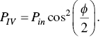
12.3.3 M–Z Interferometer AOS
Mach–Zender interferometers or M–Z interferometers are also based upon the two‐beam interference principle. Their basic construction includes two 3‐dB couplers DC1 and DC2 which are connected to two straight waveguides I and II. Thus the device consists of total of 4 ports as shown in Figure 12.3.
In a self‐pump M–Z interferometer, the two arms L1 and L2 are made of different materials with varying refractive indices n1 and n2 respectively. Along with that, the arm lengths are also of two different sizes. When light is incident in Port 1, the beam gets divided by the DC1 and two light beams with same intensity flow into arms L1 and L2. Since the two arms are different, two different phase shifts occur in them, with notations φ1 and φ2. These two‐phase shifted light signals come at DC2 and interfere and are output from Ports 3 and 4. The distribution of power among these two ports depends on the phase difference of the individual phase shifts, φ = φ1 − φ2. It can be established that for low input power, an output wave can be obtained from Port 4, but for high input powers, the phase shift nearly equals π and light is output from Port 3 and this phenomenon represents the all‐optical switching. If both the arms become identical, i.e. symmetric in nature, the phase shift equals 0 and then the interferometer cannot work as an all‐optical switch.

Figure 12.3 M–Z interferometer AOS.
Because the beams travel the measurement path only once and the beam separation can be changed according to requirement, this interferometer is thus well suited for applications like to study of flow of gases, transfer of heat, and the distribution of temperature in plasmas and flames.
12.3.4 Ring Resonator AOS
A ring resonator or RR is a type of interferometer which is based on the principle of multiple‐beam interference, similar to the Fabry–Pérot interferometer. The main working differences between the two is that the RR works on travelling‐wave interference while the FP works on standing wave interference; in the case of FP, the wave travels back and forth multiple times and in case of RR, the wave travels multiple times inside the ring. The basic structures of both interferometers are given in Figure 12.4.


Figure 12.4 (a) Multiple‐bean interference inside FP resonant cavity. (b) Multiple‐bean interference inside ring resonator.
The function of couplers C1 and C2 in the RR are same as the mirrors M1 and M2 in case of the FP interferometer. The couplers fed back the wave along the input and output paths, which mirrors are unable to do. The incident light with power Pi enters through C1 or M1 and outputs through C2 or M2 with power Pt, which are the transmitted output, and outputs from C1 or M1 with power Pr are called the reflected output.
There are two types of RRs as available from literature:
- single coupler Ring Resonator (SCRR): one common example is the all‐optical switch, which is a 1 × 1 optical switch (one straight waveguide coupled with ring through single coupler)
- double coupler Ring Resonator (DCRR): such an example is a 1 × 2 all‐optical switch.
12.3.5 Fiber Grating AOS
All macro‐scale all‐optical switches cannot fully serve the very fine practical requirements like fine tunings of wavelength and other fine jobs. For those purposes the fiber grating all‐optical switches have proved to be fruitful. The fiber grating all‐optical switches have a lot of advantages like (i) lower insertion loss, (ii) smaller dimension, (iii) comparatively less complicated structure from a fabrication point of view, and (iv) mapped with fiber system. There are a few major types of fiber gratings like Fiber Bragg grating (FBG), Chirp Fiber Grating (CFG), Phase Shift Fiber Grating (PSFG), Long‐period fiber grating (LPFG) etc.
Based on the magnitude of grating period, fiber grating can be broadly be classified into following two categories:
- Fiber Bragg Grating (FBG): Grating constant (ΛB) is less than 0.1 μm. The method of mode coupling in FBG is the interference of forward propagating and counter‐propagating waves. They together constitute reflected spectrum with a sharper bandwidth with the grating wavelength at the center. Thus these are known as optical grating of reflection type.
- Long‐Period Fiber Grating (LPFG): Grating constant (ΛL) is greater than 100 μm. Waves propagated inside core and cladding regions independently cause interference when they are superposed, provided directions of propagations are identical. It forms a transmitted profile with 20 nm approximated bandwidth with the grating wavelength at the center. Thus these are known as transmission type optical grating.
12.4 Working Methodology of Different Types of Nonlinear All‐Optical Switches
The previous section gave an overall idea of all the types of nonlinear all‐optical switches. This section provides the working principle of these switches, describing their conceptual working, their types and their various fields of applications.
12.4.1 Optical Coupler AOS
Optical coupler AOSs are classified into three types: symmetric couplers working in low incident power, symmetric couplers working in high‐power incident light with self‐phase modulation, and asymmetric couplers working with high‐power incident light with cross‐phase modulation. These are individually explained below
12.4.1.1 Symmetric Coupler Working at Low Incident Power
Symmetric couplers are those where the two wavelengths are the same as each other in all properties, so that the geometrical configurations of two waveguides are the same i.e. κ12 = κ21 = κ, and they have the same refractive indices i.e. η1 = η2 = η and β0I = β0II or δ = 0 (from Equation 12.16). When the incident light has low power and is continuous in nature, then the nonlinear effects do not come into play, that is, the light is unable to change the refractive index of the materials. Hence the parameters γ1, γ2, C1, and C2 from Equation 12.14 and Equation 12.15 are all zero and the equations reduce to


whose solutions are given by
Now cos(κz) is defined as the coupler reflectivity denoted by r and sin(κz) is defined as the coupler transmissivity denoted by t. Hence
where r and t are reflectance and transmittance for wave amplitude, r2 and t2 are power magnitudes of those parameters respectively. From the above notations, it can be said that they follow the relation (if absorption is neglected)
Also
respectively define the transmittance split factor and reflectance split factor for output powers.
If light enters only from Port 1 such that E1 ≠ 0 and E2 = 0 as shown in Figure 12.5, the coupling region length is taken to be l, and the amplitudes of the output waves at port 3 from waveguide I and at port 4 from waveguide II respectively are:
From Figure 12.5 it can be seen that the transmitted path is called t and the reflected part is called r. From Equations 12.26 and 12.27 it can be seen that the transmitted light suffers a 90° phase shift with respect to the reflected light in the direct arm. To find the respective power outputs from P3 to P4, we use the basic power‐energy relation P = |E|2. Since we know the individual energy outputs from P3 and P4, thus the respective powers can be easily calculated as

Figure 12.5 Transmitted path (t) (cross path) and reflected path (r) (bar path) inside the optical coupler.

Figure 12.6 Output light travels from I to II as a function of coupling length.
Thus it can be seen that the power distribution between the arms completely depends upon the product of the coupling coefficient κ and the length of the arm l. For a certain κ, the power output versus length variation is shown in Figure 12.6.
Here LC refers to the coupling length which is expressed by ![]() .
.
In the above case we can observe that the power outputs from the respective arms do not depend on the incident light power, but rather on the geometry of the system, hence this cannot be used to realize an all‐optical switch. The realization of all‐optical switches requires high powers which are discussed in the succeeding sections where these couplers are used with the concept of self‐phase and cross‐phase modulation.
12.4.1.2 Symmetric Coupler Working in High‐Power Incident Light with SPM
In this case a quasi‐continuous high‐power incident light enters the coupler from port 1. The input power is denoted by P0 and there exists a critical power Pc such that when the input power is lower than the critical power i.e. P0 << Pc, then the total signal emits from waveguide II. On the other hand if P0 > Pc, that is the input power is greater than the critical power, then the optical Kerr effect occurs in both the waveguides and power distribution occurs on both the arms. Since the powers are different in the two arms, hence the change in refractive indices are also different, hence different phase shifts occur within the two arms. If the phase shift crosses the threshold, then total output can only be obtained from waveguide I, as shown in Figure 12.7.
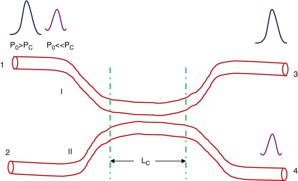
Figure 12.7 AOS with SPM technique based on symmetric coupler.
Since the coupler is symmetric, hence κ12=κ21=κ, and also the Kerr effect in both the arms is the same, hence, γ1=γ2= γ and C12 = C21 = γσ, thus the Equations 12.14 and 12.15 reduce down to
where the nonlinear parameter γ is defined by
where n2 is the nonlinear refraction coefficient, S is the effective area of light field in waveguides and k0 is the wave vector at free space. Denoting the phase and power in the individual arms by and ϕi and Pi (I = I, II,…), then the amplitude of the light wave may be expressed as
Substituting Equation 12.33 into Equation 12.30 and Equation 12.31 and setting the phase shift difference to φ = φ1 − φ2, one obtains the following equations:

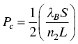
and the critical power PC is given by

If cross‐phase conduction is ignored between the arms, that is σ = 0, and using ![]() , and
, and ![]() , one obtains the final expression for critical power:
, one obtains the final expression for critical power:

Equation 12.38 depicts that for specific values of coupling length, wavelength off incoming beam and input light, critical power reduces with enhancement of nonlinear refraction coefficient and also with the decrease of waveguide working area.
Equations 12.34–12.36 can be solved analytically using elliptical functions. When light is incident on waveguide I of the coupler with a power P0, then the powers are divided into two ports, and termed as PI and PII. Then at any arbitrary point z, powers can be written as
where P0 is input power, and cn〈xτ〉 is Jacobi elliptic function where ![]() .
.
The relative power output from the two ports versus the input power curve is shown in Figure 12.8.
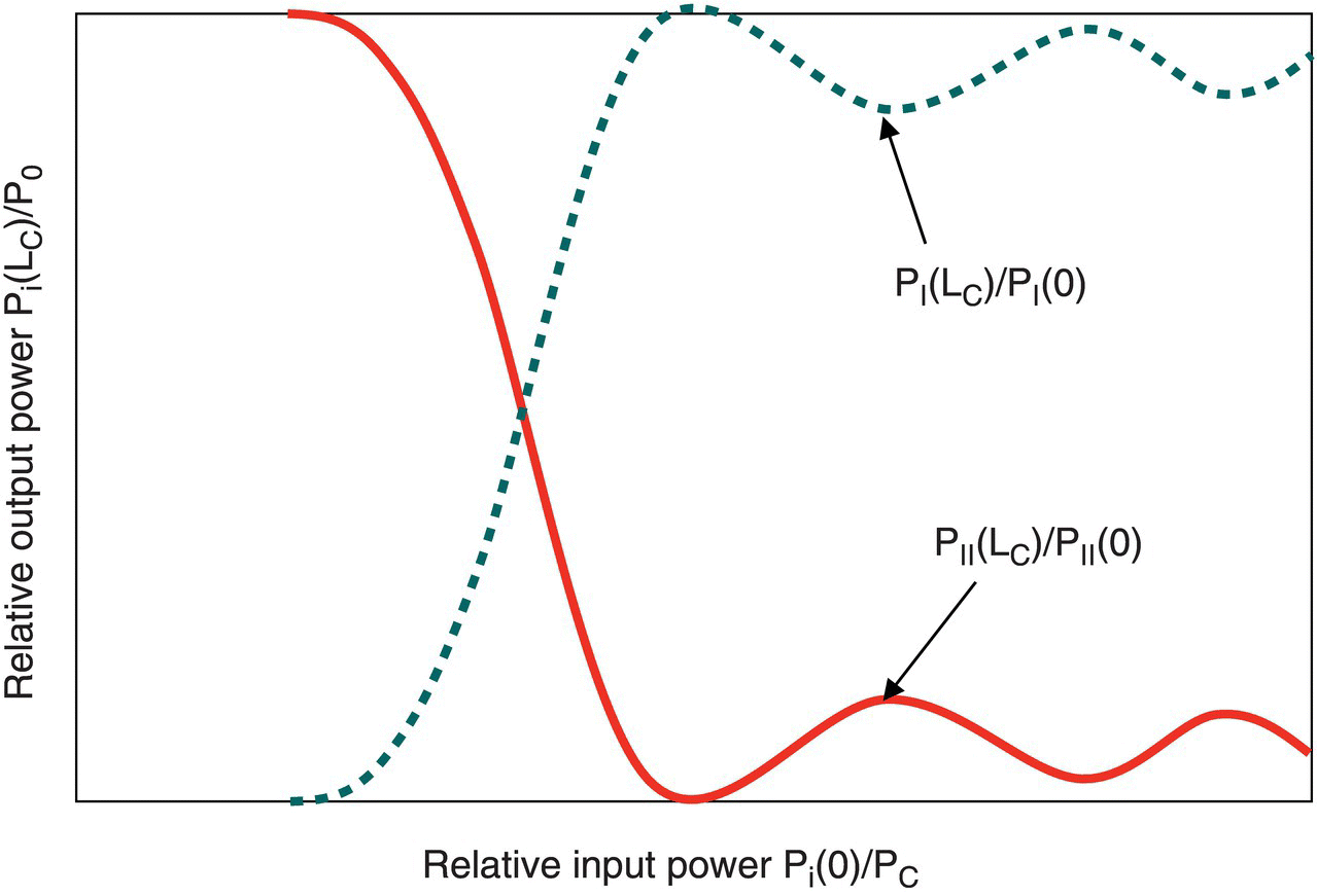
Figure 12.8 Relative output powers with relative input power.

Figure 12.9 AOS in asymmetric coupler under XPM mode.

Figure 12.10 Reflectivity and transmittance profiles with phase for low input signal.
From the plot, it may be observed that threshold switching power of the device can be given by
12.4.1.3 Asymmetric Coupler Working in High‐Power Pump Light with Cross‐phase Modulation
The setup for cross‐phase modulation using optical coupler is shown in Figure 12.9. The light as denoted by Pin is at low power and hence the nonlinearities do not occur in the waveguide for the incident signal wave. The other signal that is the pump signal denoted by Pp, which is at a different wavelength from the signal one, is a high‐power signal and thus nonlinearities start to occur in the waveguides. The corresponding reflectivity and transmittivity profiles are exhibited in Figure 12.10.
After introduction of the pump beam into the coupler, the refractive index changes in the waveguides become unequal. Since low power and quasi‐continuous signal light is used it cannot generate nonlinearities in the system and hence the terms related to nonlinearity can be neglected. Since the geometries of the guides are same, then κ12 = κ21 = κ, but since the pump is of different frequency, the coupler suffers nonlinearities, hence the power in the two different arms are different and due to the Kerr effect the refractive indices of the arms are also different, thus the propagation constant for the two are also different, i.e. β01 ≠ β02 i.e. δ ≠ 0.
Putting these into Equation 12.14 and Equation 12.15 we get
where EI and EII are the signal amplitudes. Taking derivatives of Equation 12.42 and Equation 12.43, we get


With a few mathematical computations


where
Solving the above equations using the initial values, we can get the transmission and reflection variables as
One can, therefore, easily find the expression for the amplitudes EI (l) and EII (l) as


Using the power‐energy relation, the respective powers can also be found out and is given by


If ![]() , then threshold switching power of pump wave can be written as
, then threshold switching power of pump wave can be written as

12.4.2 Sagnac Interferometer AOS
The Sagnac Interferometer AOS are classified into four types as given below.
12.4.2.1 Sagnac Interferometer (SI) Under Low Incident Power
As in the case for coupler switches, SIs also cannot function as all‐optical switches. Figure 12.2 shows the basic structure of a SI and the same structure are used as reference for present analysis. When the light is incident on Port 1 of the coupler, it gets divided equally into two light beams with powers Pin/2 which travel into the bar and cross paths of the and enter the fiber loop from Port 3 or Port 4. After one trip through the loop, no phase shift occurs. At the ports they are again separated into two light beams, which then again pass through the bar and cross paths and output from Port 1 and Port 2. At each output port, the power of the two beams depends on the difference of phases of the two light beams. If the phase difference between the beams is an integral multiple of π or (2mπ), then it is called constructive interference and the power output is the added power of the individual light beams. If the phase difference is, however, an odd multiple of π or (2m+1) π, then destructive interference occurs and the output power is the difference of the individual light beam powers. Symmetric Sagnac Interferometer cannot be used to make the all‐optical switch. The mathematical explanation is given as follows:
SI is made of symmetric coupler having coupling length l and coefficient κ. The nonlinear loop has a length L. Using coupled mode theory, we can obtain
If wavelength of input wave from Port 1 is λ, then we can formulate boundary conditions as
Wave amplitudes of port 3 and port 4 are respectively written in the form
The two light beams propagate back and forth within the loop, that is, in the clockwise and anticlockwise directions. Let the respective refractive indices of the loop medium for the light beams be ncl and nccl. After complete rotation, phase shifts are
Therefore, field amplitudes of two beams passing through bar path and cross paths respectively to reach Port 1 are
Therefore, net field at Port 1 is
Consequently the power at Port 1 is given by
The reflectivity and transmissivity of the system are defined by


where Δn indicates difference of refractive indices, Δφ is the phase difference.
For low power signal, Δn = 0, thus Δφ = 0. Then
Thus it can be seen that for low input incident light power, the output depends on the κl product and not on the input power and hence cannot be realized as all‐optical switch.
12.4.2.2 Sagnac Interferometer AOS with Non‐3dB Coupler
A non‐3dB coupler is used with the SI to induce asymmetry to the system. The setup is shown in Figure 12.11. A light incident on the input port of the SI reaches the output ports 3 and 4 with different powers which enter the loop in counter‐propagating directions. After one complete cycle, the lights produce a phase shift which is equal to π for high signal powers. When the beams reach the input ports of the system, they interfere with each other, and all the light transfers from the reflected port to the transmitted port. This is how an AOS is realized. However, under high nonlinearity and large power splitting conditions, the required signal power can be a lot less.

Figure 12.11 AOS in nonlinear SI with non‐3dB coupler working at SPM mode.
For splitting ratio Cr, clockwise beam and the anticlockwise beam powers can be respectively expressed as
where Cr = r2 = cos2(κl), 1 − Cr = t2 = 1 − r2 = 1 − cos2(κl) = sin2(κl).
For high incident power, both the cross‐phase and self‐phase modulations have to be considered, therefore the RI of the beams are given by
Therefore change in RI can be given by
Thus if Cr = 1/2, R=1 and T =0 which indicates total power output from reflected port only. For other values of Cr, the power in the two beams are different and hence the difference in RI as well as the phase difference are also non‐zero i.e. Δn = 0 and Δφ = 0. Thus light will output in parts from both the reflected and transmitted ports. To achieve complete switching, the condition for is that the difference in RI should be ![]() . From that the expression for threshold input power can be given as
. From that the expression for threshold input power can be given as

12.4.2.3 Sagnac Interferometer AOS in Cross‐Phase Modulation
The signal and pump waves are input of the system through a WDM coupler. The wavelengths of the signal and the pump are not same. Moreover, the power of the signal is lower than that of the pump. Hence the 3‐dB coupler is symmetric to the signal light but asymmetric to the pump light since it is of high power. Thus, as described above, the pump wave splits into two different beams with different powers and hence with different RIs.
When the input wave is very strong, output power is directed from Port 1 to Port 2. Assuming the pump power to be Pp and the splitting ratio to be Cpr, clockwise light is indicated by Ppcl and anticlockwise by Ppccl.
For high‐power pump light, both xPM (cross‐phase modulation) Kerr effect and SPM (self‐phase modulation) Kerr effect are taken into consideration. Moreover there is an additional XPM Kerr effect induced from the addition of the signal and pump power, hence the RIs for the clockwise and anticlockwise directions are given by Equations 12.72 and 12.73.
From the above equations, the difference in RI can be obtained as

Following the same argument for Cpr as given in the preceding section, the threshold input power is given by

12.4.2.4 Sagnac Interferometer AOS with Optical Amplifier
The setup is made by simply attaching a bidirectional EDFA in the fiber loop near the end of the coupler [37] as shown in Figure 12.12. All the operations remain same as before, just the amount of the two separate beam powers change, which are given by
where Pin is input power, Cr is the splitting ratio for bar path of coupler and G is amplifier gain.
The difference in RIs is given by

Figure 12.12 AOS in SI with optical amplifier placed asymmetrically.
Source: Richardson et al. [37] / Institution of Electrical Engineers.
Considering the condition for switching, ![]() , the threshold switching power is given by
, the threshold switching power is given by
When Cr = 1/2, the expression reduces to

12.4.3 M–Z Interferometer AOS
Keeping the basic structure same the M–Z Interferometer is mainly classified into types which are
- M–Z interferometer AOS with different arm materials
- M–Z interferometer AOS with different arm lengths.
Both of these are explained in detail [38–41]. The basic structure of an M–Z interferometer is shown in Figure 12.3.
12.4.3.1 M–Z Interferometer AOS with Different Arm Materials
This setup is same as the one shown in Figure 12.3 but with both the arms made of different nonlinear optical materials. Hence the lengths of the arms L1 = L2 = L, but due to different materials, the nonlinear RIs are not same to each other n12 ≠ n22. The incident light has a power Pin which induces unequal changes in the RIs and induces different phase shifts φ1 ≠ φ2 where φ1 = k0Δn1L and φ2 = k0Δn2L. Thus the phase difference φ = φ2 − φ1 ≠ 0.
A 3‐dB coupler is used, hence κz = π/4 and ![]() Hence the respective amplitude and power outputs (using the power‐energy relation) from Ports 3 and 4 can be written as
Hence the respective amplitude and power outputs (using the power‐energy relation) from Ports 3 and 4 can be written as

From the above equations it can be seen that for φ = 0, the output PIII = 0 and all the output is obtained from Port 4 that is PIV = Pin. For φ = π, PIII = Pin and PIV = 0, thus the condition for all‐optical switching is that the difference of phase should be equals to π.
Assuming that the linear RIs of the two arms are nearly equal to each other, and then the change in nonlinear RIs can be written as
where S is the cross‐sectional area. The individual beam phase shifts are given by
phase difference is given by
If n21>>n22 and ![]() , then the phase difference can be written as
, then the phase difference can be written as
Since the condition for all‐optical switching is, hence the threshold input power for all‐optical switching is
12.4.3.2 M–Z Interferometer All‐Optical Switch with Different Arm Lengths
The setup for this system is shown in Figure 12.13. Both the arms have same nonlinear RIs, hence n1 = n2 = n, but the arms have different lengths and the difference in length is given by ΔL = L1 − L2 ≈ L1 (assuming L1>>L2).
Since a 3‐dB coupler is used, the light splits equally in both the arms and the individual phase shifts and the phase difference are given by
Figure 12.13 M–Z interferometer AOS with different arm length and same arm material.

The condition for all‐optical switching is given by φ = π, therefore threshold input power can be given by
Henceforth, as the difference of arm length widens, switching power starts to decrease.
12.4.4 Ring Resonator AOS
Ring Resonators [42–46] are mainly divided into two types:
- AOS in M–Z Interferometer coupled with SCRR
- AOS in DCRR.
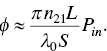
12.4.4.1 AOS in M–Z Interferometer Coupled with SCRR
This setup is a modification to the M–Z interferometer to reduce the required input power. The setup is shown in Figure 12.14. It consists of a single coupler ring resonator (SCRR). The light inputs from Port 1 through the straight waveguide with amplitude EI. EIV is field amplitude at Port 4, where input light comes into cavity of the ring from the coupler. EII and EIII are the amplitudes at Ports 3 and 4. The output EIII is the transformed output E1 with phase shift φ = φ3 − φ1.
Therefore field amplitude equation may be formulated as
Figure 12.14 Structure of AOS in M–Z interferometer coupled with ring cavity (RC).
where r and t have usual significances mentioned earlier, ϕ is phase shift for unit circle propagation, α is the absorption coefficient, ‘a’ is the loss rate for unit propagation, and l is ring perimeter.
From the above equations, the field amplitude ratios are obtained as


The amplification coefficient and finesse of the ring cavity are given by the expression


Now from Equation (104) and from Equation (105), φ can be defined as

Thus from here the transmittance can be defined as

The T versus ϕ curve is shown in Figure 12.15.
Now to calculate the threshold power, let the length of the loop be l and the Kerr effect induced nonlinear phase shift ϕ is proportional to the input power P2, thus the change of ϕ with respect to PII is given by


Figure 12.15 Transmittance (T) profile with phase shift (ϕ) for SCRR.
Since ![]() hence
hence

Integrating with the limits we get

Thus the threshold power can be given as
Thus
In terms of maximum finesse
12.4.4.2 AOS in DCRR
Basic structure of a DCRR is shown in Figure 12.16. For these structures the reflectivities r1 and r2 are kept high (→1) so as to keep maximum energies within the ring cavity. If the light input power is low then the phase shift is zero and thus the light outputs from Output Port 2, however if the light power is high, then the phase shift is π and the output is obtained from Output Port 1.
Assuming the input field amplitude to be Ein, the individual port field amplitudes are given by

Figure 12.16 Double‐coupler‐ring‐resonator AOS with one IP and two OPs.
where ri and ti (i=1, 2) are the reflectivity and transmissivity of the couplers 1 and 2 respectively. Similarly a1 = exp (−α1l1/2) and a2 = exp (−α2l2/2) are the loss coefficients of the respective couplers where α1, α2 and l1, l2 are the absorption and lengths of the left half ring and right half ring respectively. Thus for the whole ring, α = α1 + α2, l = l1 + l2 and ϕ = ϕ1 + ϕ2.
Assuming a2 ≈ a ≈ 1, r1 = r2 = r, and neglecting absorption loss, we get

As before the amplification factor and finesse are defined by


With r1 = r2 = r → 1 and a → 1 and ϕ = 2mπ(m = 1, 2, 3…), the maximum amplification factor and finesse can be approximated to
Taking into consideration of optical Kerr effect, and length of half‐ring as l1 = l2 = l/2, phase shift for unit circle propagation is
where S is the cross‐sectional area.
For all‐optical switching condition that is φ = π, the threshold input power can be given as
Apart from switching power, ring resonator AOS also has switching time property index (s). It depends on two factors: the photon lifetime of ring cavity (τc) and the nonlinear response time of material (τf):
12.4.5 Fiber Grating AOS
Fiber Grating all‐optical switches [47–51] are mainly divided into two groups, namely:
- single nonlinear FBG AOS
- single nonlinear LPFG AOS.
Other than these there are two special types of grating optical switches, which are described below.
12.4.5.1 Single Nonlinear FBG AOS
This is the simplest FBG structure to be used as a nonlinear switch. Every Bragg Grating has a particular central wavelength which is known as the Bragg Wavelength (λB). If the incident signal contains any wavelength which is equal to the Bragg Wavelength, then according to the Bragg Condition, that particular wavelength is reflected back while the others are transmitted. Thus if a narrowband signal with a wavelength equal to Bragg wavelength is incident in the input port of the FBG (λi), then by the principle of energy conservation, whole incident light (λf) is reflected back and the transmission is zero.
The relationship between the propagation constants according to the conservation of momentum principle is given by
where βi and βf are propagation constants of incident and reflected waves respectively. Under Bragg condition and principle of energy conservation
which implies

Using the Bragg grating constant notation (ΛB) it can be written as

Since the incident and reflected signals are opposite to each other, hence
Grating wavelength can be written as
Refractive index of uniform fiber Bragg grating can be expressed as

where z is displacement along fiber axis direction, ![]() is the modulation amplitude of average effective grating refractive index.
is the modulation amplitude of average effective grating refractive index.
The field variations are given by
where  is the detuning parameter.
In steady state, FBG couple‐mode equations are given by

where κ is the coupling coefficient given by
where s is the contrast ratio of refractive index modulation.
Assuming the grating length to be L, the amplitude reflectivity of grating is given by
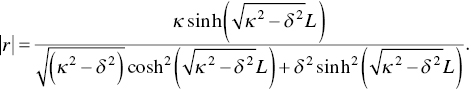
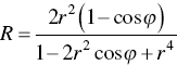
Energy reflectivity of grating given by, R = |r|2 is given by

For δ=0, FBG has maximum reflectivity is obtained at λ = λB which is given by
The reflected spectrum bandwidth of FBG (Δλ0) is described as interval between two wavelengths where null reflectivity occurs at both sides of grating wavelength. It is given by

Assuming κL < < π

where N is the total number of grating given by

Introducing optical Kerr effect under self‐phase modulation, change of refractive index of the fiber is given by
where n0 is linear refractive index, n2 is the nonlinear refraction coefficient, P is input light power.
Change of grating wavelength is
The necessary condition for realizing switching process under input power is the shift of grating wavelength, i.e.
Thus the threshold switching power can be given as
12.4.5.2 Single Nonlinear LPFG AOS
The name suggests LPFG refers to the fiber gratings with the period of grating longer than the normal gratings. Coupling between core and cladding modes are considered for light propagation inside LPFG. For coupling between fundamental mode LP01 and mth order mode LP0m, their propagation constants βco and βcl are related as

where βg is the propagation constant of fiber grating, kL is the grating constant of LPFG.
In terms of difference between the RIs of core and cladding, it can be written as

where λL = ΛLΔng is the grating wavelength of LPFG; Δng is the effective refractive index difference between fundamental mode and cladding mode of fiber, i.e.,
The detuning is defined as

where

The reflected spectrum bandwidth Δλ0 is given by

With the assumption κL < < π, it can be expressed as


Figure 12.17 Transmission spectrum of LPFG.
where
The reflection curve of LPFG is given in Figure 12.17.
In SPM mode, when grating wavelength becomes equal to incident wavelength, transmittance of grating structure is minimum. With increasing signal power, the transmission spectrum moves towards longer wavelength by the effect of the optical Kerr effect. If grating wavelength becomes half of bandwidth, then transmittance becomes maximum, and a corresponding similar change is attained by transmitted power.
Due to the induced Kerr effect by the signal power, changes in core and cladding RIs are given by
The change in cladding can be neglected, hence
Therefore
Hence the shift in grating wavelength is given by
At ![]() , optical switching is accomplished, hence
, optical switching is accomplished, hence

Figure 12.18 Optical bistable switching device consisted of two same FBGs.
Finally the threshold switching power is given by
There are two other types of special configurations for FBGs, which are:
- nonlinear fiber connected LPFG‐pair AOS
- nonlinear fiber connected FBG‐pair optical bistable switch.
The first one uses the same concept as the amplifier connected Sagnac interferometer, whose main purpose is to decrease the input threshold power considerably. The nonlinear fiber here consists of an EDF which acts as an amplifier at the 1550 nm window with a pump source at 980 nm. With the use of an amplifier with the FBG, the same properties of an FBG all‐optical switch can be achieved but can be operated with much lower input optical power which thus makes the system more economical.
The second type is the nonlinear FC FBG‐pair OBS, which consists of two symmetric FBGs connected by a rare‐earth‐doped nonlinear fiber. This ultimately constitutes nonlinear F‐P interferometer. Multiple‐beam interference is formed through back‐and‐forth movement of signal beam. Change of both refractive index and also of phase take place when the beam interacts with the nonlinear medium. Figure 12.18 shows the optical bistable switch.
For lower switching power, Yb3+‐doped fiber is referred by most researchers, owing to its higher speed of switching and smaller absorption.
12.5 Nanoscale AOS
From all the above description of different all‐optical switches, we can see that there is a common factor in every formula for the input power, which is
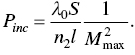
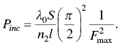
where all symbols have known significances. In addition, for RR, there is ring finesse Fmax in the denominator. From the above expression, certain conclusions can be derived as
- The threshold power can be reduced by increasing the RI of the material. But by increasing the RI, the absorption increases which can be harmful for the signal transmission as greater absorption greatly reduces the signal power throughout the transmission.
- To decrease effective cross‐section of waveguide S. Reduction of switching power from kW to mW can happen if S can be reduced from μm2 to nm2. Thus nanoscale waveguides are required for the realization of all‐optical switching device.
- Extension of length L is beneficial for switching power reduction. But overall size of device will increase considerably. Thus micro‐ring structures can be used. To offset the shortage of material with small n2, the ring structure can increase the nonlinearity. High finesse Fmax ring is expected to be used for this purpose.
Therefore, using nanoscale materials and structures is a fantastic way to reduce switching power of all‐optical switches. In addition, small‐scale devices can also help in reducing the processing time as light has to travel lesser distances in small‐scale devices. The nanoscale all‐optical switch is based on nanophotonics [52–59]. Research on photonic crystals leads the path [60–64] towards development of filter‐based optical switches.
The main focus of nanophotonics is to study the interaction between optical radiations in the nanoscale with nano‐scale optical materials and devices. The most important nano‐materials are the materials which have periodicity in the microcosm scale, such as the low‐dimensional nanoelectronic materials which have the properties of quantum confinement (owing to their dimensional similarity with de‐Broglie wavelength) which include quantum 2D device (well), quantum 1D device (wire) and quantum dots etc. They in general consist of two alternative bandgap materials (preferably compound semiconductor so that tailoring of bandgap can be achieved as per requirement), and also grating optical structures (e.g., photonic crystals) materials consisting of two dielectric materials alternately with diverse refractive indices; in addition the conductive nano‐materials with a conductor‐insulator/semi‐insulator interface in which transfer of information occurs between incident optical wave and periodic e.m. field to form stable/quasi‐stable Surface Plasmon Polariton (SPP). One of the widely acceptable nano‐structure for all‐optical switch is confined transmission line in submicron dimension (waveguide in that regime) with similar cross‐section and the interferometers made by it, particularly the micro‐ring.
12.6 Future Scope and Conclusion
Optical communication is the future of telecommunication. There are several advantages of optical systems over electrical systems. Moreover, with the help of optical systems, quantum communications can be achieved, which can be even more useful and faithful for long‐distance and minimum‐loss communications. But the full deployment of optical systems has not not possible till now due for various reasons such as long fiber losses, bending losses, unavailability of good processing systems, and lack of good optical hardware like switches, modulators, amplifiers at all frequencies. Though some of these are available for macro systems, for micro systems they are still being developed and hence fully independent optical systems are yet to be fully deployed.
All‐optical switches play a very important role in the hardware processing of optical signals. They are used to route signals through different channels and send them to several measurement devices, make divisions in optical power and much more. After studying and analyzing all the above all‐optical switches, it can be seen that all‐optical switches have been greatly developed in recent research and hence are paving the way for modern‐day optical communications as well as quantum communications.
With the advent of more advanced technologies all other optical devices like nano‐amplifiers and nano‐processors will be extremely crucial for the operation of an optical circuit. Thus the study of nanophotonics – photonic crystals – which has been mentioned in the preceding section is the main interest of research in the field of photonics. Silicon Integrated Photonics paves the way for low‐cost and efficient nanophotonics, and in coming days more such materials with better optical properties can be used for the research and manufacturing of nano‐optical circuits and devices.
To conclude, we can say that the present electrical systems are running out of opportunities to be as useful as they used to be with respect to the requirement of bandwidths, higher security, undisturbed connections, and much more. Optical systems help to provide those features and thus prove much more advantageous than electrical systems. Moreover, if free‐space optics can be made more efficient, then they would completely replace the present electrical systems and fully independent optical systems can be deployed and used both commercially and industrially.
Bibliography
- 1 D. Botez and G.J. Herskowitz. Components for optical communications systems: A review. Proceedings of the IEEE, 68(6):689–731, 1980.
- 2 R. Alferness. Guided‐wave devices for optical communication. IEEE Journal of Quantum Electronics, 17(6):946–959, 1981.
- 3 N. Tsukada and T. Nakayama. Polarization‐insensitive integrated‐optical switches: A new approach. IEEE Journal of Quantum Electronics, 17(6):959–964, 1981.
- 4 A. Milton and W. Burns. Mode coupling in tapered optical waveguide structures and electro‐optic switches. IEEE Transactions on Circuits and Systems, 26(12):1020–1028, 1979.
- 5 T.H. Chu, S. Yamada Ishida, and Y. Arakawa. Compact 1 × N thermo‐optic switches based on silicon photonic wire waveguides. Optics Express, 13(25):10109–10114, 2005.
- 6 H.C. Tapalian, J.‐P. Laine, and P.A. Lane. Thermooptical switches using coated microsphere resonators. IEEE Photonics Technology Letters, 14(8):1118–1120, 2002.
- 7 S. Ghafari, M.R. Forouzeshfard, and Z. Vafapour. Thermo optical switching and sensing applications of an infrared metamaterial. IEEE Sensors Journal, 20(6):3235–3241, 2019.
- 8 L. Sirleto, G. Coppola, M. Iodice, M. Casalino, M. Gioffrè, and I. Rendina. Thermo‐optical switches. In B. Li and S.J Chua, editors, Optical Switches, 61–96. Cambridge, Woodhead, 2010.
- 9 M. Bass, E.W. Van Stryland, D.R. Williams and W.L. Wolfe. Handbook of Optics, Volume II – Devices, Measurements, and Properties. McGraw‐Hill.
- 10 M. Delgado‐Pinar, D. Zalvidea, A. Diez, P. Perez‐Millan, and M. Andres. Q‐switching of an all‐fiber laser by acousto‐optic modulation of a fiber Bragg grating. Optics Express, 14(3):1106–1112, 2006.
- 11 D.A. Smith, R.S. Chakravarthy, Z. Bao, J.E. Baran, J.L. Jackel, A. d’Alessandro, D.J. Fritz, S.H. Huang, X.Y. Zou, Hwang, S.‐M., A.E. Willner, and K.D. Li. Evolution of the acousto‐optic wavelength routing switch. Journal of Lightwave Technology, 14(6):1005–1019, 1996.
- 12 S. Antonov, A. Vainer, V. Proklov, and Y. Rezvov. Switch multiplexer of fiber‐optic channels based on multibeam acousto‐optic diffraction. Applied Optics, 48(7):C171–C181, 2009.
- 13 D.F. Nelson and M. Lax. New symmetry for acousto‐optic scattering. Physical Review Letters, 24:378–380, 1970.
- 14 J. Chapelle and L. Tauel. Theorie de la diffusion de la lumiere par les cristeaux fortement piezoelectriques. Comptes Rendus de l'Académie des Science, 240:743, 1955.
- 15 G.H. Heilmeier, L.A. Zanoni, and L.A. Barton. Dynamic scattering: A new electrooptic effect in certain classes of nematic liquid crystals. Proceedings of IEEE, 56(7):1162–1171, 1968.
- 16 G.H. Heilmeier and L.A. Zanoni. Guest‐host interactions in nematic liquid crystals. A new electro‐optic effect. Applied Physics Letters, 13:91–92, 1968.
- 17 S.‐T. Wu and J.D. Margerum. Liquid crystal dyes with high solubility and large dielectric anisotropy. Applied Physics Letters, 64:2191–2193, 1994.
- 18 J.J. Wysocki, J. Adams, and W. Haas. Electric‐field‐induced phase change in cholesteric liquid crystals. Physical Review Letters, 20(19):1024, 1968.
- 19 G.H. Heilmeier and J.E. Goldmacher. A new electric‐field‐controlled reflective optical storage effect in mixed‐liquid crystal systems. Applied Physics Letters, 13:132–133, 1968.
- 20 M. Schadt and W. Helfrich.Voltage‐dependent optical activity of a twisted nematic liquid crystal. Applied Physics Letters, 18:127–128, 1971.
- 21 M.F. Schiekel and K. Fahrenschon.Deformation of nematic liquid crystals with vertical orientation in electrical fields. Applied Physics Letters, 19:391–393, 1971.
- 22 K. Lu and B.E.A. Saleh. Complex amplitude reflectance of the liquid crystal light valve. Applied Optics, 30:2354–2362, 1991.
- 23 A. Sasaki, K. Kurahashi, and T. Takagi. Liquid‐crystal thermo‐optic effects and two new information display devices. Journal of Applied Physics. 45:4356, 1974.
- 24 F.J. Khan. Orientation of liquid crystals by surface coupling agents. Applied Physics Letters, 22:386, 1973.
- 25 H. Ren and S.‐T. Wu. Inhomogeneous nanoscale polymer‐dispersed liquid crystals with gradient refractive index. Applied Physics Letters, 81:3537–3539, 2002.
- 26 D.‐K. Yang, L.‐C. Chien, and J.W. Doane.Cholesteric liquid crystal/polymer dispersion for haze‐free light shutters. Applied Physics Letters, 60:3102–3104, 1992.
- 27 C. Li. All‐Optical Switches Based on Nonlinear Optics. Beijing, Science Press, 2015.
- 28 H.M. Gibbs.Optical Bistability: Controlling Light with Light. New York, Academic Press, 1985.
- 29 S. Divya, I. Sebastian, V.P.N. Nampoori, P. Radhakrishnan, and A. Mujeeb.Power and composition dependent non‐linear optical switching of TiO2‐SiO2 nano composites. In International Conference on Optical Engineering, Belgaum, India, 1–5, 2012.
- 30 A. Elgamri and B. Rawat.Optical switching using optical Kerr non‐linear effect on photonic crystal fiber. In International Conference on Signal Processing and Communication, Noida, 4–9, 2016.
- 31 W. Liu, C. Yang, M. Liu, W. Yu, Y. Zhang, M. Lei, and Z. Wei. Bidirectional all‐optical switches based on highly nonlinear optical fibers. Europhysics Letters, 118(3):34004, 2017.
- 32 A. Granpayeh, H. Habibiyan, and P. Parvin. Photonic crystal directional coupler for all‐optical switching, tunable multi/demultiplexing and beam splitting applications. Journal of Modern Optics, 66(4):359–366, 2018.
- 33 Y. Akihama and K. Hane. Single and multiple optical switches that use freestanding silicon nanowire waveguide couplers. Light: Science & Applications, 1(6), e16, 2012.
- 34 C. Setterlind and L. Thylen. Directional coupler switches with optical gain. IEEE Journal of Quantum Electronics, 22(5):595–602, 1986.
- 35 S. Slussarenko, V. D’Ambrosio, B. Piccirillo, L. Marrucci, and E. Santamato. The Polarizing Sagnac Interferometer: a tool for light orbital angular momentum sorting and spin‐orbit photon processing. Optics Express, 18(26):27205–27216, 2010.
- 36 M. Jinno and T. Matsumoto. Demonstration of laser‐diode‐pumped ultrafast all‐optical switching in a nonlinear Sagnac interferometer. Electronics Letters, 27(1):75–76, 1991.
- 37 D.J. Richardson, R.L. Laming, and D.N. Payne. Very low threshold Sagnac switch incorporating an Erbium doped fiber amplifier. Electronics Letters, 26(21):1779–1781, 1990.
- 38 A. Stanley, G. Singh, J. Eke, and H. Tsuda. Mach‐Zehnder interferometer: A review of a perfect all‐optical switching structure. In Proceedings of the International Conference on Recent Cognizance in Wireless Communication & Image Processing, 415–425, 2016.
- 39 M. Islam and M. Barsha. Mach Zehnder interferometer (MZI) as a switch for all optical network. IEEE International Conference on Innovation in Engineering and Technology, 27–28 Dec, Dhaka, Bangladesh, 2018.
- 40 Z. Lu, D. Celo, H. Mehrvar, E. Bernier, and L. Chrostowski. High‐performance silicon photonic tri‐state switch based on balanced nested Mach‐Zehnder interferometer. Scientific Reports, 7(1), 2017.
- 41 T. Hirokawa, M. Saeidi, S. Pillai, A. Nguyen‐Le, L. Theogarajan, A. Saleh, and C. Schow. A wavelength‐selective multiwavelength ring‐assisted Mach‐Zehnder interferometer switch. Journal of Lightwave Technology, 38(22):6292–6298, 2020.
- 42 J.E. Heebner and R.W. Boyd. Enhanced all‐optical switching by use of a nonlinear fiber ring resonator. Optics Letters, 24(12):847–849, 1999.
- 43 M. Ghadrdan and M.A. Mansouri‐Birjandi. Implementation of all‐optical switch based on nonlinear photonic crystal ring resonator with embedding metallic nanowires in the ring resonators. Optical and Quantum Electronics, 48(5), 2016.
- 44 A.H.J. Yang and D. Erickson. Optofluidic ring resonator switch for optical particle transport. Lab on a Chip, 10(6):769–774, 2010.
- 45 J.K. Rakshit, T. Chattopadhyay, and J.N. Roy. Design of ring resonator based all optical switch for logic and arithmetic operations – A theoretical study. Optik – International Journal for Light and Electron Optics, 124(23):6048–6057, 2013.
- 46 J.E. Heebner and R.W. Boyd. Enhanced all‐optical switching by use of a nonlinear fiber ring resonator. Optics Letters, 24(12):847–849, 1999.
- 47 G.R. Broderick, D. Taverner, and D.J. Richardson. Nonlinear switching in fiber Bragg gratings. Optics Express, 3(11):447–453, 1998.
- 48 D. Taverner, G.R. Broderick, and D.J. Richardson. Nonlinear self‐switching and multiple gap‐soliton formation in a fiber Bragg grating. Optics Letters, 23(5):328–330, 1998.
- 49 R.H. Stolen, W.A. Reed, K.S. Kim, and G.T. Harvey. Measurement of the nonlinear refractive index oflong dispersion‐shifted fibers by self‐phase modulation at 1.55 μm. Journal of Lightwave Technology, 16(6):1006–1012, 1998.
- 50 M. Janos, J. Arkwright, and Z. Brodzeli. Low power nonlinear response of Yb3+ doped optical fibre Bragg gratings. Electronics Letters, 33(25):2150–2151, 1997.
- 51 B. Guan and S. Liu. Erbium‐doped fiber Bragg grating based all‐optical switch. In IEEE CLEO/Pacific Rim 2003, The 5th Pacific Rim Conference on Lasers and Electro‐Optics, Taipei, Taiwan, 2003.
- 52 R.V. Almeida, A. Carlos, and M. Lipson. All‐optical control of light on a silicon chip. Nature, 431(28):1081–1084, 2004.
- 53 M. Lipson. Overcoming the limitations of microelectronics using Si nanophotonics: solving the coupling, modulation and switching challenges. Nanotechnology, 15(10):S622–S627, 2004.
- 54 C. Koos, P. Vorreau, T. Vallaitis, and P. Dumon. All‐optical high‐speed signal processing with silicon–organic hybrid slot waveguides. Nature Photonics, 3(4):216–219, 2009.
- 55 A. Martınez, J. Blasco, P. Sanchis, et al. Ultrafast all‐optical switching in a silicon‐nanocrystalbased silicon slot waveguide at telecom wavelengths. Nano Letters, 10(4):1506–1511, 2010.
- 56 K. Tajima. All‐optical switch with switch‐off time unrestricted by carrier lifetime. Japanese Journal of Applied Physics, 32(12A):Ll746–Ll748, 1993.
- 57 K. Asakawa. Fabrication and characterization of photonic crystal slab waveguides and application to ultra‐fast all‐optical switching devices. IEEE ICTON, 1:193–197, 2003.
- 58 H. Nakamura et al. Ultra‐fast photonic crystal/quantum dot all optical switch for futurephotonic networks. Optics Express, 12(26):6606–6614, 2004.
- 59 Z. Qiang, W. Zhou, and R.A. Soref. Optical add‐drop filters based on photonic crystal ring resonators. Optics Express, 15(4):1823–1831, 2007.
- 60 A. Deyasi, U. Dey, S. Das, S. De, and A. Sarkar. Computing photonic bandgap from dispersion relation for TM mode propagation inside metamaterial‐based 1D PhC. Micro and Nanosystems, 12:201–208, 2020.
- 61 A. Deyasi and A. Sarkar. Computing optical bandwidth of bandpass filter using metamaterial‐based defected 1D PhC. AIP Conference Proceedings, 2072:020003, 2019.
- 62 A. Deyasi and A. Sarkar. Variation of optical bandwidth in defected ternary photonic crystal under different polarization conditions. International Journal of Nanoparticles, 10(1&2):27–34, 2018.
- 63 A. Deyasi and A. Sarkar. THz bandpass filter design using metamaterial‐based defected 1D photonic crystal structure. In A. Biswas, A. Banerjee, A. Acharyya, H. Inokawa, J. Nath Roy, editors, Emerging Trends in Terahertz Solid‐State Physics and Devices, 1:1–21, 2020.
- 64 A. Deyasi. Computation of electromagnetic bandgap in two‐dimensional photonic crystal. In A. Deyasi, editor, Foundations in Photonics and Fiber‐Optics, 12:257–278, 2019.