CHAPTER 10
Cross Talk in Transmission Lines
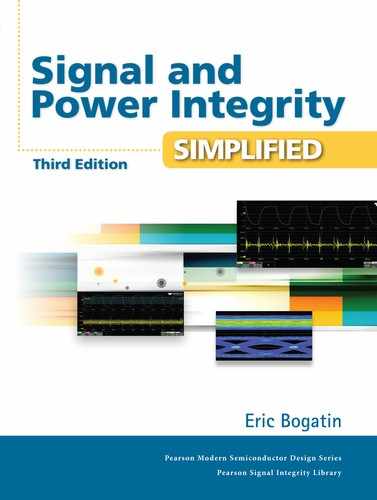
Cross talk is one of the six families of signal-integrity problems. It is the transfer of an unwanted signal from one net to an adjacent net, and it occurs between every pair of nets. A net includes both the signal and the return path, and it connects one or more nodes in a system. We typically call the net with the source of the noise the active net or the aggressor net. The net on which the noise is generated is called the quiet net or the victim net.
TIP
Cross talk is an effect that happens between the signal and return paths of one net and the signal and return paths of a second net. The entire signal–return path loop is important—not just the signal path.
In single-ended digital signaling systems, the noise margin is typically about 15% of the total signal-voltage swing, but it varies among device families. Of this 15%, about one-third, or 5%, of the signal swing is typically allocated to cross talk. If the signal swing were 3.3 v, the maximum allocated cross talk might be about 160 mV. This is a good starting place for the maximum allowable cross-talk noise. Unfortunately, the magnitude of the noise generated in typical traces on a board can often be larger than 5%. This is why it is important to be able to predict the magnitude of cross talk, identify the origin of excessive noise, and actively work to minimize the cross talk in the design of packages, connectors, and board-level interconnects. Understanding the origin of the problem and how to design interconnects with reduced cross talk is increasingly important as rise time decreases.
Figure 10-1 shows the noise on the receiver of a quiet line when aggressor lines on either side have 3.3-v signals. In this example, the noise at the receiver is more than 300 mV.

Figure 10-1 Simulated cross talk on a quiet line with aggressor lines on either side. Each line is a source-series terminated 50-Ohm microstrip in FR4 with a 10-mil line and space. Simulated with Mentor Graphics HyperLynx.
In mixed-signal systems, such as with analog or rf elements, the acceptable noise on sensitive lines can be much less than 5% the signal swing. It can be as low as –100 dB below the signal swing, which is 0.001% of the signal. When evaluating design rules for reduced cross talk, the first step is to establish an acceptable specification, keeping in mind that, generally, the lower the acceptable cross talk, the lower the achievable interconnect density, and the higher the potential cost of the system. Be aware of requirements that recommend substantially below 5% maximum allowable coupled noise. Always verify if they really need such low cross talk, as it generally will not be free.
10.1 Superposition
Superposition is an important principle in signal integrity and is critical when dealing with cross talk. Superposition is a property of all linear, passive systems, of which interconnects are a subset. It basically says multiple signals on the same net do not interact and are completely independent of each other. The amount of voltage that might couple onto a quiet net from an active net is completely independent of the voltage that might already be present on the quiet net.
TIP
The noise coupled to a quite line is independent of any signal that might also be present.
Suppose the noise generated on a quiet line were 150 mV from a 3.3-v driver when the voltage level on the quiet line is 0 v. There would also be 150 mV of noise generated on the quiet line when the quiet line is driven directly by a driver to a level of 3.3 v. The total voltage appearing on the quiet line would be the direct sum of the signals that may be present and the coupled noise. If there are two active nets coupling noise to the same quiet line, the amount of noise appearing on the quiet line would be the sum of the two noise sources. Of course, they may have a different time dependency based on the voltage pattern on the two active lines.
Based on superposition, if we know the coupled noise when the quiet line has no additional signal on it, we can determine the total voltage on the quiet line by adding the coupled noise and any signal that might also be present.
Once the noise is on the quiet line, it is subject to the same behavior as the signal: Once generated at some location on the quiet line, it will immediately propagate and see the same impedance, and it will suffer reflections and distortions from any impedance discontinuities that may be present in the quiet line.
TIP
Noise voltages on a quiet line behave exactly as signal voltages. Once generated on the quiet line, they will propagate and be subject to reflections from discontinuities.
If a quiet line has an active line on either side of it, and each active line couples an equal amount of noise to the quiet line, the maximum allowable noise between one pair of lines would be ½ × 5% = 2.5%. In a bused topology, it is important to be able to calculate the worst-case total number of adjacent traces that might couple to determine the worst-case coupled noise. This will put a limit on how much noise might be allowable between just two traces.
10.2 Origin of Coupling: Capacitance and Inductance
When a signal propagates down a transmission line, there are electric-field lines between the signal and return paths and rings of magnetic-field lines around the signal- and return-path conductors. These fields are not confined to the immediate space between the signal and return paths. Rather, they spread out into the surrounding volume. We call these fields that spread out fringe fields.
TIP
As a rough rule of thumb, the capacitance contributed by the fringe fields in a 50-Ohm microstrip in FR4 is about equal to the capacitance from the field lines that are directly beneath the signal line.
Of course, the fringe fields drop off very quickly as we move farther away from the conductors. Figure 10-2 shows the fringe fields between a signal path and a return path and how they might interact with a second net when it is far away and then when it is close.

Figure 10-2 Fringe fields near a signal line. When a second trace is far away, there is little fringe-field coupling and little cross talk. When the second net is in the vicinity of the fringe fields, there can be excessive coupling and cross talk.
If we are unfortunate enough to route another signal and its return path in a region where there are still large fringe fields from another net, the second trace may pick up noise from these fringe fields. The only way noise will be picked up in the quiet line is when the signal voltage and current in the active line change. This will cause current to flow through the changing electrics as displacement current and as induced currents from the changing magnetic fields.
Engineering interconnects to reduce cross talk is about reducing the overlap of the electric and magnetic fringe fields between the two signal- and return-path pairs. This is usually accomplished in two ways. First, the spacing between the two signal lines can be increased. Second, the return planes can be brought closer to the signal lines. This will couple the fringe field lines closer to the plane, and less will leak out to the adjacent signal line.
TIP
Ultimately, it is the fringe fields that cause cross talk. An important way to minimize cross talk is to space nets far enough apart so their fringe fields are reduced to acceptable levels. Another design feature is to bring the return plane closer to the signal lines to confine the fringe fields more in the vicinity of the signal line.
While the actual coupling mechanism is by electric and magnetic fields, we can approximation this coupling by using capacitor and mutual inductor circuit elements.
Between every two nets in a system, there will always be some combination of capacitive coupling and inductive coupling arising from these fringe fields. We refer to the coupling capacitance and the coupling inductance as the mutual capacitance and the mutual inductance. Obviously, if we were to move the two adjacent signal- and return-path traces farther apart, the mutual-capacitance and mutual-inductance parameter values would decrease.
Being able to predict the cross talk based on the geometry is an important step in evaluating how well a design will meet the performance specification. This means being able to translate the geometry of the interconnects into the equivalent mutual capacitance and inductance and relating how these two terms contribute to the coupled noise.
Though both mutual capacitance and mutual inductance play a role in cross talk, there are two regimes to consider. When the return path is a wide, uniform plane, as is the case for most coupled transmission lines in a circuit board, the capacitively coupled current and inductively coupled current are of the same order of magnitude, and both must be considered to accurately predict the amount of cross talk. This is the regime of cross talk in transmission lines on circuit boards as part of a bus, and the noise will have a special signature.
When the return path is not a wide uniform plane but is a single lead in a package or a single pin in a connector, there is still capacitive and inductive coupling, but in this case, the inductively coupled currents are much larger than the capacitively coupled currents. In this regime, the noise behavior is dominated by the inductively coupled currents. The noise on the quiet line is driven by a dI/dt in the active net, which usually happens at the rising and falling edges of the signal when the driver switches. This is why this type of noise is usually referred to as switching noise.
These two extremes are considered separately.
10.3 Cross Talk in Transmission Lines: NEXT and FEXT
The noise between two adjacent transmission lines can be measured in the configuration shown in Figure 10-3. A signal is injected into one end of the line, with the far end terminated to eliminate the reflection at the end of the line. The voltage noise is measured on the two ends of the adjacent quiet line. Connecting the ends of the quiet line to the input channels of the fast scope will effectively terminate the quiet line. Figure 10-4 shows the measured voltage noise in a quiet line adjacent to an active signal line that is driven by a fast-rising edge. In this case, the two 50-Ohm microstrip transmission lines are about 4 inches long, with a spacing about equal to their line width. The ends of each line are terminated in 50 Ohms, so the reflections are negligible.

Figure 10-3 Configuration to measure the cross talk between an active net and a quiet net, looking on the near end and far end of the quiet line.

Figure 10-4 Measured noise on the quiet line when the active line is driven with a 200-mV, 50-psec rise-time signal. Measured with an Agilent DCA TDR and GigaTest Labs Probe Station.
The measured noise voltage has a very different pattern on each end. To distinguish the two ends, we label the end nearest the source the near end and the end farthest from the source the far end. The ends are also defined in terms of the direction the signal is traveling. The far end is in the forward direction to the signal-propagation direction. The near end is in the backward direction to the signal-propagation direction.
When the ends of the lines are terminated so multiple reflections do not play a role, the patterns of noise appearing at the near and far ends have a special shape. The near-end noise rises up quickly to a constant value. It stays up at this level for a time equal to twice the time delay of the coupling length and then drops down. We label the constant, saturated amount of near-end noise the near-end cross talk (or NEXT) coefficient. This is the ratio of the near-end noise voltage to the signal voltage. In the example shown here, the incident signal voltage is 200 mV, and the measured noise voltage is 13 mV. This makes the NEXT coefficient = 13 mV/200 mV = 6.5%.
The NEXT value is special in that it is defined as the near-end noise when the coupling length is long enough to reach the constant, flat value and in the special case of matched terminations. Changing the terminations at the end of the lines will not change the coupled noise into the quiet line. However, the backward-traveling noise, when it hits the end of the line, may reflect if the termination is not matched. When the terminations are matched to the characteristic impedance of the line, the NEXT is a measure of the noise generated in the line. Once this is known, the impact on this voltage when it encounters a different termination can easily be estimated.
Obviously, the value of the NEXT will depend on the separation of the traces. Unfortunately, the only way of decreasing the NEXT is to move the traces farther apart or bring the return plane closer to the signal traces.
The far end has a signature very different from the near end. There is no far-end noise until one time of flight after the signal enters the active line. Then it comes out very rapidly and lasts for a short time. The width of the pulse is the rise time of the signal. The peak voltage value is labeled the far-end cross talk. In the example above, the far-end cross talk voltage is about 60 mV. The FEXT coefficient is the ratio of the peak far-end voltage to the signal voltage. In this example, with a signal of 200 mV, the FEXT coefficient is 60 mV/ 200 mV = 30%. This is a huge amount of noise.
If the terminations are not matched, and reflections affect the magnitude of the noise appearing at the ends, we still refer to the far-end cross talk, but the magnitude is no longer related to FEXT. This coefficient is the special case when the terminations are matched.
TIP
Four factors decrease the FEXT: bringing the return plane closer, decreasing the coupling length, increasing the rise time, and moving the traces farther apart.
10.4 Describing Cross Talk
One way of describing the coupling that contributes to cross talk is in terms of the equivalent circuit model of the coupled lines. This model allows simulations that take into account the specific geometry and the terminations when predicting voltage waveforms. Two different models are generally used to model the coupling in transmission lines.
An ideal, distributed coupled transmission-line model for two lines describes a differential pair. The terms that describe the coupling are the odd- and even-mode impedances and the odd- and even-mode time delays. These four terms describe all the transmission-line and coupling effects. Many simulation engines, such as SPICE engines, especially those that have an integrated 2D field solver, use this type of model. The bandwidth of this model is as high as the bandwidth of an ideal lossless transmission line. This is the same model as a differential pair and is reviewed in detail in Chapter 11, “Differential Pairs and Differential Impedance.”
An alternative, widely used model to describe coupling uses the n-section lumped-circuit-model approximation. In this model, each of the two transmission lines is described with an n-section lumped-circuit model, and the coupling between them is described with mutual-capacitor and mutual-inductor elements. The equivalent circuit model of just one section is shown in Figure 10-5.

Figure 10-5 Equivalent circuit model of one section of an n-section coupled transmission-line model.
The actual capacitance and loop inductance between the signal and return paths and their mutual values are distributed uniformly down the length of the transmission lines. For uniform, coupled transmission lines, the per-length values describe the transmission lines and the coupling. As shown below, these values can be displayed in a matrix, and this matrix formalism can be scaled and expanded to represent any number of coupled transmission lines. In some simulators, this matrix representation is the basis of describing the coupling, even though the actual simulation engine uses a true, distributed-transmission-line model.
We can approximate this distributed behavior by small, discrete lumped elements placed periodically down the length. The approximation gets better and better as we make the discrete lumped elements smaller. The number of sections needed, as shown in a Chapter 7, “The Physical Basis of Transmission Lines,” depends on the required bandwidth and the time delay, with the minimum number being:
where:
n = minimum number of lumped sections for an accurate model
BW = required bandwidth of the model, in GHz
TD = time delay of each transmission line, in nsec
Two coupled transmission lines can be described with two independent n-section lumped-circuit models. If the lines are symmetrical, the L and C values in each segment will be the same for each line. To this uncoupled model, we need to add the coupling. In each section, the coupling capacitance can be modeled as a capacitor between the signal paths. The coupling inductance can be modeled as a mutual inductor between each of the loop inductors in the n-section model.
Each single-ended transmission line is described by a capacitance per length, CL, and a loop self-inductance per length, LL. The coupling is described by a mutual capacitance per length, CML, and a loop mutual inductance per length, LML. For a pair of uniform transmission lines, the mutual capacitance and mutual inductance are distributed uniformly down the two lines.
TIP
Everything about the two coupled transmission lines can be described by these four line parameters. When there are more than two transmission lines, the model can be scaled directly, but it looks more complicated. Between every pair of sections of the transmission lines, there is a mutual capacitor. Between every pair of signal- and return-loop sections, there is a mutual inductor.
Each of the mutual capacitors and loop mutual inductors scales with length, and we refer to their mutual capacitance and mutual inductance per length. To keep track of each of these additional mutual capacitors and inductors, we can take advantage of a simple formalism based on matrices.
10.5 The SPICE Capacitance Matrix
For a collection of multiple transmission lines, we can label each signal path with an index number. If there are five lines, for example, we would label each one from 1 to 5. The return path, by convention, we label as conductor 0. An example of the cross section of five conductors and a common return plane is shown in Figure 10-6. We first look at the capacitor elements. Later in this chapter, we look at the inductor elements.

Figure 10-6 Five coupled transmission lines, in cross section, with each conductor labeled using the index convention.
Every pair of conductors in the collection has a capacitance between them. For every signal line, there is a capacitor to the return path. Between every pair of signal lines, there is a coupling capacitor. To keep track of all the pairs, we can label the capacitors based on the index numbers. The capacitance between conductors 1 and 2 is labeled C12, and the capacitance between capacitors 2 and 4 is labeled C24. The capacitance between the signal line and the return we might label as C10 or C30.
To take advantage of the powerful formalism of matrix notation, we rename the capacitor labels that describe the capacitance between the signal paths and their return paths. Instead of C10, we reserve the diagonal element for the capacitance between the signal and its return path and label it C11. Likewise, the other capacitors between the signals and their returns become C22, C33, C44, and C55. In this way, we end up with a 5 × 5 matrix of capacitors that labels the capacitance between every pair of conductors. The equivalent circuit and corresponding matrix of parameter values are shown in Figure 10-7.

Figure 10-7 Equivalent capacitance model of five coupled transmission lines and the corresponding matrix of capacitance parameter values.
Of course, even though there is a matrix entry for C14 and C41, it is the same capacitor value, and there is only one instance of this capacitor in the model.
In the capacitor matrix, the diagonal elements are the capacitance between the signal and the return paths. The off-diagonal elements are the coupling or mutual capacitance. For uniform transmission lines, each matrix element is the capacitance per length, usually in units of pF/inch.
The matrix is a handy, convenient, compact way of keeping track of all the capacitor values. This matrix is often called the SPICE capacitance matrix to distinguish it from some of the other matrices. It is a place to store the parameter values for the SPICE equivalent circuit model, shown earlier in this chapter. Each matrix element represents the value of a capacitor that would be present in the complete circuit model for the coupled transmission lines.
Each element is the capacitance per length. To construct the actual transmission lines’ approximate model, we would first identify how many sections are needed in the lumped-circuit model, from n > 10 × BW × TD. From the length of the transmission lines and the number of sections required, the length of each section can be calculated as Length per section = Len/n. The value of the capacitor for each section is the matrix element of the capacitance per length times the length of each section. For example, the coupling capacitance of each section would be C21 × Len/n.
The actual values for each capacitor-matrix element can be found by either calculation or by measurement. Few approximations are very good. Rather, a few simple rules of thumb can be used, and when a more accurate value of the coupling capacitance is required, a 2D field solver should be used. Many field solver tools are commercially available; they are easy to use and generally very accurate. An example of the SPICE capacitance matrix for a collection of five microstrip conductors, as calculated with a 2D field solver, is shown in Figure 10-8.

Figure 10-8 Five coupled transmission lines, each of 5-mil line width and 5-mil space and the SPICE capacitance matrix, in pF/inch, calculated with the Ansoft SI2D field-solver tool.
When it is difficult to get a good physical feel for the values of the capacitance-matrix elements and how quickly they drop off by just looking at the numbers, the matrix can be plotted in 3D. The vertical axis is the magnitude of the capacitance. These same matrix elements are shown in Figure 10-9. At a glance, it is apparent that all the diagonal elements have about the same values, and the off-diagonal elements drop off very fast.

Figure 10-9 Plotting the SPICE capacitance-matrix elements, showing how quickly off-diagonal elements drop off.
In this particular example, the conductors are 50-Ohm microstrips, with 5-mil line width and 5-mil space, placed as close together as possible. We see that the coupling between conductors 1 and 3 is negligible compared to that between conductors 1 and 2. The farther apart the traces, the more rapidly the off-diagonal elements drop off. This is a direct indication of how quickly the fringe electric fields drop off with spacing.
In the SPICE capacitance matrix, it is important to keep in mind that each element is the parameter value of a circuit element that appears in an equivalent circuit model. The value of each element is a direct measure of the amount of capacitive coupling between the two conductors. This will directly determine, for example, the capacitively coupled current that would flow between each pair of conductors for a given dV/dt. The larger the matrix element, the larger the capacitive coupling, and the more fringe fields between the conductors.
TIP
In coupled transmission lines, the size of the off-diagonal element should always be compared with the diagonal element. In this geometry example of five coupled 50-Ohm lines, with a spacing equal to the line width (the tightest spacing manufacturable), the relative coupling between adjacent traces is about 5%. The coupling between one trace and the trace two traces away is down to less than 0.6%. These are good values to remember as a rough rule of thumb.
The physical configuration of the traces will affect the parameter values, but for a given configuration of traces, the circuit model itself will not change as the geometry of the traces changes. Obviously, if we move the traces farther apart, the parameter values will decrease.
If we change the line width of one line, to first order, it will affect the diagonal element of that line and the coupling between that line and the adjacent traces on either side. However, it may also affect, to second or third order, the coupling between the lines on either side of it. The only way to know for sure is to put in the numbers with a 2D field solver.
10.6 The Maxwell Capacitance Matrix and 2D Field Solvers
Unfortunately, there is more than one capacitance matrix, and this creates confusion. Earlier in this chapter, we introduced the SPICE capacitance matrix, whose elements were the parameter values of the equivalent circuit model for the coupled lines. There is also a capacitance matrix that is the result of a field-solver calculation; it is referred to as the Maxwell capacitance matrix. Even though they are both called capacitance matrices, their definitions are different.
A field solver is basically a tool that solves one or more of Maxwell’s Equations for a specific set of boundary conditions. A circuit topology for the collection of conductors is assumed, and from the fields, all the parameter values are calculated. The equation that is solved to calculate the capacitances of an array of conductors is LaPlace’s Equation. In its simplest differential form, it is:
This differential equation is solved under the specific geometry boundary conditions of the conductors and dielectric materials. Solving this equation allows for the calculation of the electric fields at every point in space.
For example, suppose there is a collection of five conductors, as shown in Figure 10-10. Conductor 0 is defined as the ground reference and is always at 0-v potential. To calculate the capacitance between the conductors, there are six steps:

Figure 10-10 Conductor setup to calculate the capacitance matrix for this collection of transmission lines using a 2D field solver that solves LaPlace’s Equation.
1. A 1-v potential is set on conductor k, and the potential of every other conductor is set to 0 v.
2. Given this boundary condition, LaPlace’s Equation is solved to find the potential everywhere in space.
3. Once the potential is solved, the electric field is calculated at the surface of each conductor, from:
4. The total charge is calculated on each conductor by integrating the electric field on the surface of each conductor:

5. From the charge on each conductor, the capacitance is calculated from the definition of the Maxwell Capacitance matrix:
6. This process is repeated with a 1-v potential sequentially placed on each of the conductors.
The definition of the Maxwell capacitance-matrix elements is different from the SPICE capacitance-matrix elements. The SPICE matrix elements are the parameter values for the corresponding equivalent circuit model. The value of each element is a direct measure of the amount of capacitively coupled current that would flow between each pair of conductors for a given dV/dt between them.
The Maxwell capacitance-matrix elements are really defined based on:
Each capacitance-matrix element between two conductors is a measure of how much excess charge will be on one conductor when the other is at a 1-v potential and all other conductors are grounded. This is a very specialized condition and gives rise to much confusion.
Suppose a 1-v potential is placed on conductor 3, and all the other conductors are at 0-v potential. To do this will require placing some extra plus charge on conductor 3 to raise it to a 1-v potential with respect to ground. This plus charge will attract some negative charge to all the other nearby conductors. The negative charge will come out of the ground reservoir to which each other conductor is connected. How much charge is attracted to each of the other conductors is a measure of how much capacitive coupling there is to the conductor with the 1 v applied. The charge distribution is illustrated in Figure 10-11.

Figure 10-11 Charge distribution for the five conductors with conductor 3 set to 1 v and all others at ground potential.
From the definition of the Maxwell capacitance matrix, the capacitance between conductor 3 and the reference ground, which is the diagonal element, is the ratio of the charge on conductor 3, Q3, and the voltage on it, V3 = 1 v. This is the charge on conductor 3 when all the other conductors are also connected to ground. This capacitance is often called the loaded capacitance of conductor 3:
The loaded capacitance will always be larger than the SPICE diagonal capacitance.
When there is plus charge on conductor 3 to raise it up to the 1-v potential, the charge induced on all the other conductors is negative. Even though all the other conductors are at ground potential, they will have some net negative charge due to the coupling to the conductor with the 1 v.
TIP
The diagonal elements of the Maxwell capacitance matrix are the loaded capacitances of each conductor. It is not just the capacitance to the return path, the ground reference; it is the capacitance to the return path and to all the other conductors that are also tied to ground. This is not the same as the diagonal element of the SPICE capacitance matrix, which just includes the coupling of the conductor to the return path and not to any other signal path.
By the definition of the Maxwell capacitance matrix, the off-diagonal-matrix element between conductor 3 and 2 will be:
TIP
Since the charge induced on conductor 2 is negative and the induced charge on every other conductor is also negative, every off-diagonal capacitor-matrix element must be negative.
The negative sign really means that the induced charge on conductor 2 will be negative when a 1-v potential is placed on conductor 3.
An example of the Maxwell capacitance matrix for a collection of five microstrip traces is shown in Figure 10-12. At first glance, it is bizarre to see capacitance values that are negative. What could it possibly mean to have negative capacitances? Is this an inductance? In fact, they are negative because they are not SPICE capacitance values but Maxwell capacitance values, and the definition of the Maxwell capacitor-matrix elements is different from the SPICE elements.

Figure 10-12 Maxwell capacitance matrix, in pF/inch, for the collection of five closely spaced, 50-Ohm transmission lines calculated with Ansoft’s SI2D field solver.
The output from most commercially available field solvers is typically in the form of Maxwell capacitance values. This is usually because the software developer who wrote the code did not really understand the end user’s applications and did not realize that most signal-integrity engineers want to see the SPICE capacitance-matrix elements. The Maxwell capacitance matrix is not wrong; it is just not an engineer’s first choice of what to see.
It is very easy to convert from one matrix to the other. The off-diagonal elements are very similar, with just the sign difference:
The off-diagonals relate to the number of field lines that couple the two conductors and directly relate to the capacitively coupled current that might flow between the conductors for a given dV/dt between them.
However, the diagonals are a little more complicated. The diagonal elements of the Maxwell matrix are the loaded capacitance of each conductor. The diagonal elements of the SPICE matrix are the capacitance between just the diagonal conductor and the return path. The SPICE diagonal element is counting only the field lines coupling between the signal line to the return path. Based on this comparison, diagonal elements of the SPICE and Maxwell matrices can be converted by:


The easiest way to determine which matrix is reported by the field solver is to look for negative signs. If there are negative signs, it’s usually not numerical accuracy; it is the Maxwell capacitance matrix.
In either matrix, the off-diagonal elements are a direct measure of the coupling between signal lines and the strength of the fringe fields that couple the conductors. The greater the spacing, the fewer the fringe-field lines between the traces and the lower the coupling. In both matrices, the physical presence of any conductor between two traces will affect the field lines between them and will be taken into account by the matrix-element values.
Each matrix element will depend on the presence of the other conductors. For example, for two conductors and their return path, the diagonal SPICE capacitance of one line, C11, will depend on the position of the adjacent conductor. C11 is the capacitance of line 1 to the return path. If we bring the adjacent trace in proximity, it will begin to steal some of the fringe-field lines between line 1 and the return and decrease C11. This is illustrated in Figure 10-13.

Figure 10-13 Variation of the diagonal and off-diagonal elements of the SPICE capacitance matrix and the loaded capacitance of conductor 1 as the spacing between the two 5-mil-wide, 50-Ohm lines increases. Simulated with Ansoft’s SI2D.
When the spacing is more than about two line widths or four dielectric thicknesses, the presence of the adjacent trace has very little impact on the diagonal element of the SPICE capacitance matrix.
Since the loaded capacitance of line 1 is a measure of all the fringe-field lines between the signal line and all the other conductors, it doesn’t change much as the adjacent trace is brought closer. Field lines not going from 1 to the return, stolen by trace 2, are accounted for by the new field lines between 1 and 2.
The off-diagonal elements will also depend on the geometry and the presence of other conductors. If the spacing is increased, the off-diagonal element will decrease. Also, if another conductor is added between two traces, this conductor will steal some of the field lines between the two conductors and decrease the off-diagonal SPICE capacitance element.
Figure 10-14 shows three geometry configurations and the resulting SPICE capacitance-matrix element that is calculated. In each case, the signal line is 5 mils wide and roughly 50 Ohms.

Figure 10-14 Three geometries and the corresponding capacitance matrix elements between the two signal lines. The presence of the metal between the conductors decreases the capacitive coupling about 35%.
TIP
When the spacing is also 5 mils wide, the coupling capacitance is 0.155 pF/in. This is about 5% of the on-diagonal element of 2.8 pF/inch. When the spacing is increased to 15 mils, so the spacing is three times the width, the capacitive coupling is 0.024 pF/inch, or 0.9% of the diagonal element. If another 5-mil-wide trace is added in this space, the coupling capacitance between the two outer conductors is reduced to 0.016 pF/inch, or 0.6% of the on-diagonal element.
By adding a conductor between the two signal lines, the coupling capacitance between them is reduced. This is the basis of the use of guard traces, discussed in detail later in this chapter. Of course, we have only considered one type of coupling; there is also inductive coupling to consider.
10.7 The Inductance Matrix
Just as a matrix is used to store all the capacitor values in a collection of signal- and return-path conductors, a matrix is used to store the values of the loop self-inductance and the loop mutual inductances associated with a collection of conductors. It is important to keep in mind that the inductance elements are loop inductances. As the signal propagates down a transmission line, the current loop travels down the signal path and immediately returns through the return path. This current loop is probing the loop inductance in the immediate vicinity of the edge of the signal transition. Of course, the loop self-inductance is related to the partial self-inductances of the signal and return paths, and their mutual inductance, by:
where:
Lloop = loop inductance per length of the transmission line
Lself-signal = partial self-inductance per length of the signal path
Lself-return = partial self-inductance per length of the return path
Lmutual = partial mutual inductance per length between the signal and return paths
In the inductance matrix, the diagonal elements are the loop self-inductances of each signal and return path. The off-diagonal elements are the loop mutual inductance between every pair of signal and return paths. The units are in inductance per length, typically nH/inch.
For example, the five microstrip traces above have an inductance matrix shown in Figure 10-15. When plotted in 3D, the loop-inductance matrix reveals the basic properties of inductance. The diagonal elements—the loop self-inductances of each conductor and its return path—are all basically the same. The off-diagonal elements—the loop mutual inductances—drop off very rapidly the farther apart the pair.

Figure 10-15 Five transmission lines, each 50 Ohms and with a 5-mil width and 5-mil spacing, their inductance matrix, and the values of each matrix element as extracted using the Ansoft SI2D field solver.
The combination of the capacitance and inductance matrices contains all the information about the coupling between a collection of transmission lines. From these values, all aspects of cross talk between two or more transmission lines can be calculated. A SPICE equivalent circuit model can be built that could be used to simulate the behavior of a collection of coupled traces.
These two matrices contain all the fundamental information about the coupling between multiple transmission lines.
10.8 Cross Talk in Uniform Transmission Lines and Saturation Length
For the case of two coupled transmission lines, the C and L matrices are simple, two-by-two matrices. The off-diagonal elements describe the amount of mutual capacitance and mutual inductance. The easiest way to understand the generation of the noise in the quiet line and the particular near-end and far-end signature is to walk down the line and observe the noise coupling-over at each step.
Consider two 50-Ohm microstrip transmission lines that have some coupling distributed down their length. In addition, we will terminate the ends of the lines in their characteristic impedance of 50 Ohms to eliminate any effects from reflections. This equivalent circuit model is illustrated in Figure 10-16.

Figure 10-16 A pair of tightly coupled transmission lines and an equivalent circuit model using an n-section lumped-circuit approximation.
As a signal propagates down the active line, it will see the mutual capacitors and mutual inductors connecting it to the quiet line. The only way noise current will flow from the active line to the quiet line is through these elements, and the only way current flows through a capacitor, or is induced in a mutual inductor, is if either the voltage or current changes. This is illustrated in Figure 10-17. If the leading edge is approximated by a linear ramp with a rise time of RT, the noise is approximately proportional to V/RT and I/RT.

Figure 10-17 The only region in which coupled noise flows from the active line to the quiet line is at the signal wavefront where the voltage and current change.
TIP
As the signal propagates down the active line, the only place there is coupled-noise current to the quiet line is in the specific region where the edge of the signal is, where there is a dV/dt or a dI/dt. Everywhere else along the line, the voltage and current are constant, and there is no coupled-noise current.
The edge of the signal acts as a current source moving down the line. At any instant, the total current that flows through the mutual capacitors is:
where:
IC = capacitively coupled-noise current from the active line to the quiet line
V = signal voltage
RT = 10–90 rise time of the signal
Cm = mutual capacitance that couples over the length of the signal rise time
The total capacitance that is coupling is the capacitance along the spatial extent of the rise time, where there is a changing voltage:
where:
Cm = mutual capacitance that couples over the length of the signal rise time
CmL = mutual capacitance per length (C12)
∆x = spatial extent of the leading edge as it propagates over the active line
v = signal-propagation speed
RT = signal rise time
The total, instantaneous, capacitively coupled current injected into the quiet line is:
where:
IC = capacitively coupled-noise current from the active line to the quiet line
CmL = mutual capacitance per length (C12)
v = signal-propagation speed
RT = signal rise time
V = signal voltage
The capacitively coupled current from the active line is injected into the quiet line locally only where the edge of the signal is in the active line. Surprisingly, the coupled-noise current has a total magnitude that is independent of the rise time. The faster the rise time, the larger the dV/dt, so we would expect a larger amount of capacitively coupled current. But, the faster the rise time, the shorter the region of coupled line where there is a dV/dt and the less capacitance is available to do the coupling. The capacitively coupled current depends only on the mutual capacitance per length.
By the same analysis, the instantaneous voltage induced in the mutual inductor in the quiet line is:
where:
VL = inductively coupled-noise voltage from the active line to the quiet line
I = signal current in the active line
LmL = mutual inductance per length (L12)
v = signal-propagation speed
RT = signal rise time
Again, we see that the inductively coupled noise crosses to the quiet line only where the signal voltage is changing on the active line. Also, the amount of noise voltage generated in the quiet line does not depend on the rise time of the signal but only on the mutual inductance per length.
Four important properties emerge about the coupled-noise to the quiet line:
1. The amount of instantaneous coupled voltage and current noise depends on the signal strength. The larger the signal voltage and current, the larger the amount of instantaneously coupled noise.
2. The amount of instantaneously coupled voltage and current noise depends on the amount of coupling per length, as measured by the mutual capacitance and mutual inductance per length. If the coupling per length increases as the conductors are brought closer together, the instantaneously coupled noise will increase.
3. It appears that the higher the velocity, the higher the instantaneously coupled total current. This is due to the fact that the higher the speed, the longer the spatial extent of the rise time and the longer the region that we will see coupling at any one instant. If the velocity of the signal increases, the coupled length over which current flows will increase, and the total coupling capacitance or inductance will increase.
4. Surprisingly, the rise time of the signal does not affect the total instantaneously coupled-noise current or voltage. While it is true that the shorter rise time will increase the coupled noise through a single mutual C or L element, with a shorter rise time, the spatial extent of the edge is shorter, and there is less total mutual C and mutual L that couple at any one instant.
This last property is based on an assumption that the length of the coupled region is longer than half the spatial extent of the rise time. This is the most confusing and subtle aspect of near-end noise.
Consider a pair of coupled lines with a TD of the coupling region very long compared to the rise time of the signal. As the signal starts out from the driver and enters the coupling region, the amount of coupled noise flowing between the aggressor and victim lines will begin to increase and appear as increasing near-end noise. The near-end noise will continue to increase as long as more rising edge enters the coupling region. The near-end noise increases for a time equal to the rise time. After this period of time, the near-end noise has reached its maximum value and has “saturated.”
When the beginning of the leading edge of the signal finally leaves the coupled region, the coupled current flowing from the aggressor line to the victim line will begin to decrease. Of course, it will take one TD of the coupled region for the beginning of the rising edge to traverse the coupled region. Once the coupled current begins to decrease, at the far end of the line, it will take another TD for this reduced current to make it back to the near end and be recorded as reduced near-end noise. The near-end noise will begin to decrease in a time equal to 2 × TD from the very beginning of the near-end noise starting.
As the coupling TD between the two transmission lines is decreased, there will be a point where the near-end noise reaches its peak value, a rise time after it begins, just as it begins to decrease, 2 × TD after it enters the coupled region. This condition is that the rise time = 2 × TD. This is the condition for the coupling length being just long enough to saturate the near-end noise.
When the rise time of the signal is 2 × TD, the coupled lines are saturated. This condition is when the TD is half the rise time, or when the coupling length is half the spatial extent of the rising edge. We give this length the special name saturation length:
where:
Lensat = saturation length for near-end cross talk, in inches
RT = rise time of the signal in nsec
v = speed of the signal down the active line in inches/nsec
If the rise time is 1 nsec, in a transmission line composed of FR4, with a velocity of roughly 6 inches/nsec, the saturation length is ½ nsec × 6 inches/nsec = 3 inches. If the rise time were 100 psec, the saturation length would be only 0.3 inch. For short rise times, the saturation length is usually shorter than a typical interconnect length, and near-end noise is independent of coupled length. The saturation length is illustrated in Figure 10-18.

Figure 10-18 The saturation length is half the spatial extent of the leading edge. If the length of the coupled region is longer than the saturation length, the amount of near-end noise on the quiet line is independent of the rise time and independent of the coupling length.
Once the noise current transfers from the active line to the quiet line, it will propagate in the quiet line and give rise to the effects we see as near-end and far-end noise. Even though a constant current is transferring to the quiet line, the features of the propagation in the quiet line will shape this distributed-current source into very different patterns at the near and far ends. To understand the details of the origin of the near- and far-end signatures, we will first look at how the capacitively coupled currents behave at the two ends and then at the inductively coupled currents and add them up.
10.9 Capacitively Coupled Currents
Figure 10-19 shows the redrawn equivalent circuit model with just the mutual-capacitance elements. In this example, we assume that the coupled length is longer than the saturation length. The rising edge will act as a current source moving down the active line. Because current flows through the mutual capacitors only when there is a dV/dt, it is only at the rising edge that there is capacitively coupled current flowing into the quiet line.

Figure 10-19 Equivalent circuit model of two coupled lines just showing the coupling capacitors, the coupled current, and the spatial extent of the signal edge.
Once this current appears in the quiet line, which way will it flow? The primary factor that will determine the direction of the current flow is the impedance the noise current sees. When the noise current looks up and down the quiet line, it sees exactly the same impedance in both directions: 50 Ohms. An equal amount of noise current will flow in both the forward and backward directions.
The direction of the capacitively coupled-current loop in the quiet line is from the signal path to the return path. It is a positive voltage between the signal and return paths of the quiet line that will propagate in both directions.
As the signal initially emerges from the driver, there will be some capacitively coupled current to the quiet line. Half of this will travel backward to the near end. The other half will travel in the forward direction. The current, flowing through the terminating resistor on the near end of the quiet trace, will flow in the positive direction, from the signal path to the return path. It will start out at 0 v, and as the rising edge emerges from the driver, it will rise up. As the signal edge moves down the line, the backward-flowing capacitively coupled-noise current will continue back to the near end at a steady rate. It is as though the active signal is leaving a constant, steady amount of current flowing back toward the near end in its wake.
After a time equal to the rise time, the current appearing at the near end will reach its peak value. After the beginning of the rising edge in the active line has left the coupled region and reached the far-end terminating resistor, the coupled-noise current will begin to decrease, taking a time equal to the rise time. There is still the backward-moving current in the quiet line that has yet to reach the near end of the quiet line. It will continue flowing back to the near end of the quiet line, taking additional time equal to the time delay, TD, of the coupled region.
The signature of the near-end, capacitively coupled current is a rise up to a constant value in a time equal to the signal’s rise time and staying at a constant value lasting for a time equal to 2 × TD – rise time, and then falling to zero in a rise time. This is illustrated in Figure 10-20.

Figure 10-20 Typical signature of the capacitively coupled voltage at the near end of the quiet line, through the terminating resistor.
The magnitude of the saturated, capacitively coupled current at the near end will be:
where:
IC = capacitively coupled, saturated noise current at the near end of the quiet line
CmL = mutual capacitance per length (C12)
v = signal-propagation speed
V = signal voltage
½ factor = comes from half the current going to the near end and the other half to the far end
½ factor = accounts for the backward-flowing noise current spread out over 2 × TD
The second factor of ½ comes from the fact that the current source is moving in the forward direction, while the near end’s portion of the induced current is moving in the backward direction. In every short interval of time, a total amount of charge is transferred into the quiet line, which is moving in the backward direction—but over a spatial extent that is expanding in both directions. The total current, which is the charge that flows past a point per unit time, is spread over two units of time.
While half the capacitively coupled-noise current is flowing backward to the near end, the other half of the capacitively coupled-noise current is moving in the forward direction. The forward current in the quiet line is moving to the far end at exactly the same speed as the signal edge is moving to the far end in the active line. At each step along its path, half of it is added to the already present noise moving in the forward direction. It is as though the forward-moving capacitively coupled current were growing like a snowball down a hill, building up more and more each step along its way.
At the far end, no current is present until the signal edge reaches the far end. Coincident with the signal hitting the far end, the forward-moving, capacitively coupled current reaches the far end. This current is flowing from the signal path to the return path. Through the terminating resistor across the quiet line, the voltage drop will be in the positive direction.
Since the capacitively coupled current to the quiet line scales with dV/dt, the actual noise profile in the quiet line, moving to the far end, will be the derivative of the signal edge. If the signal edge is a linear ramp, the capacitively coupled-noise current will be a short rectangular pulse, lasting for a time equal to the rise time. The capacitively induced noise signature at the far end of the quiet line is illustrated in Figure 10-21.

Figure 10-21 Typical signature of the capacitively coupled voltage at the far end of the quiet line, through the terminating resistor.
The total amount of current that couples over from the active to the quiet line will be concentrated in this narrow pulse. The magnitude of the current pulse, translated into a voltage by the terminating resistor, will be:
where:
IC = total capacitively coupled-noise current from the active line to the quiet line
½ factor = fraction of capacitively coupled current moving to the far end
CmL = mutual capacitance per length (C12)
RT = signal rise time
V = signal voltage
The magnitude of the capacitively coupled current at the far end scales directly with the mutual capacitance per length and with the coupled length of the pair of lines, and it scales inversely with the rise time. A shorter rise time will increase the far-end noise.
Unlike the backward-propagating noise, the far-end propagating noise voltage will scale with the length of the coupled region and will scale inversely with the rise time of the signal. The current direction for the forward-propagating capacitively coupled current will be in the positive direction, from the signal line to the return path, therefore generating a positive voltage across the terminating resistor.
10.10 Inductively Coupled Currents
Inductively coupled currents behave in a similar way to capacitively coupled currents. These currents are driven by a dI/dt in the active line through the mutual inductor, which creates a voltage in the quiet line. The noise voltage induced in the quiet line will see an impedance and will drive an associated current.
The changing current in the active line is moving from the signal to the return path, propagating down the line. If the direction of propagation is from left to right, the direction of the current loop is clockwise, as a signal-return path loop. This is also the direction of the increasing current, the dI/dt in the active line, a clockwise circulating loop. This changing current loop will ultimately induce a current loop in the quiet line. But in what direction will be the induced current loop? Will it be in the same direction as the signal current loop, the clockwise direction, or the opposite direction, the counterclockwise direction?
The direction of the induced current loop is based on the results of Maxwell’s Equations. While it is tedious to go through the analysis to determine the direction of the induced current, it is easy to remember based on Lentz’s Law, which states that the direction of the induced current loop in the quiet line will be in the opposite direction of the inducing current loop in the active line.
The direction of the induced current loop in the quiet line will be circulating in the counterclockwise direction, located in the quiet line right where the signal edge is in the active line. This is illustrated in Figure 10-22.
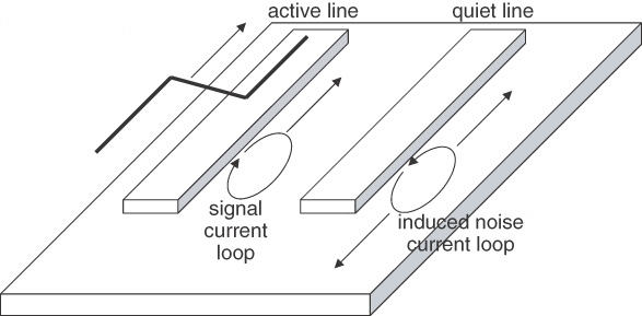
Figure 10-22 A dI/dt in the active line induces a voltage in the quiet line, which in turn creates a dI/dt in the quiet line. Half of the current loop will propagate in each direction in the quiet line.
Once this counterclockwise current loop is generated in the quiet line, which direction will it propagate? Looking up and down the line, it will see the same impedance, so it will propagate equal amounts of current in the two directions. This is a very subtle and confusing point. Half of the current in the induced current loop in the quiet line will propagate back to the near end. The other half of the current in the induced current loop in the quiet line will propagate in the forward direction.
Moving in the backward direction, the counterclockwise current loop will be flowing from the signal path to the return path. This is the same direction the capacitively coupled currents flow. At the near end, the capacitively and inductively coupled-noise currents will add together.
TIP
Moving in the forward direction, the counterclockwise current loop in the quiet line is flowing from the return path up to the signal path. The capacitively coupled and inductively coupled currents circulate in the opposite directions when they are moving in the forward direction. When the coupled currents reach the far-end terminating resistor on the quiet line, the net current through the terminating resistor will be the difference between the capacitively coupled current and the inductively coupled current.
The backward-moving inductively coupled-noise current will have exactly the same signature as the capacitively generated noise current. It will start out at zero and rise up as the signal emerges from the driver. After a time equal to the rise time, the backward-flowing current will reach a constant value and stay at that level. The signal edge will act as a current source for the inductively coupled currents and couple a constant amount of current as it propagates down the whole coupled length.
After the rising edge of the signal has just reached the terminating resistor at the far end of the active line, there will still be backward-flowing inductively coupled-noise current in the quiet line. It will take another TD for all this current to finally flow back to the near end of the quiet line. The current flows for the backward- and forward-moving noise currents are shown in Figure 10-23.

Figure 10-23 Induced-current loops propagating in the forward and backward direction as the signal in the active trace moves down the line.
Moving in the forward direction, the inductively coupled noise will travel at the same speed as the signal edge in the active line. Each step along the way, there will be more and more inductively coupled noise current coupled over. The far-end noise will grow larger with coupled length. The shape of the inductively coupled current at the far end will be the derivative of the rise time, as it is directly proportional to the dI/dt of the signal.
The direction of the inductively coupled current at the far end is counterclockwise, from the return path up to the signal path. This is the opposite direction of the capacitively coupled current. At the far end, the capacitively coupled noise and inductively coupled noise will be in opposite directions. The net far-end noise will actually be the difference between the two.
10.11 Near-End Cross Talk
The near-end noise voltage is related to the net coupled current through the terminating resistor on the near end. The general signature of the waveform is displayed in Figure 10-24. There are four important features of the near-end noise:
1. If the coupling length is longer than the saturation length, the noise voltage will reach a constant value. The magnitude of this maximum voltage level is defined as the near-end cross-talk (NEXT) value. It is usually reported as a ratio of the near-end noise voltage in the quiet line to the signal in the active line. If the voltage on the active line is Va and the maximum backward voltage on the quiet line is Vb, the NEXT is NEXT = Vb/Va. In addition, this ratio is also defined as the near-end cross-talk coefficient, kb = Vb/Va.
2. If the coupling length is shorter than the saturation length, the voltage will peak at a value less than the NEXT. The actual noise-voltage level will be the peak value, scaled by the actual coupling length to the saturation length. For example, if the saturation length is 6 inches—that is, the signal has a rise time of 2 nsec in FR4—and the coupled length is 4 inches, the near-end noise is Vb /Va = NEXT × 4 inches/6 inches = NEXT × 0.66. Figure 10-25 shows examples of the near-end noise for coupling lengths ranging from 20% of the saturation length to two times the saturation length.
3. The total time the near-end noise lasts is 2 × TD. If the time delay for the coupled region is 1 nsec, the near-end noise will last 2 nsec.
4. The turn on for the near-end noise is the rise time of the signal.


Figure 10-25 Near-end cross-talk voltage as the coupling length increases from 20% of the saturation length to two times the saturation length. Rise time is 1 nsec, speed is 6.6 inch/nsec, and saturation length is 0.5 nsec × 6.6 in/nsec = 3.3 inches. Simulated with Mentor Graphics HyperLynx.
The magnitude of the NEXT will depend on the mutual capacitance and the mutual inductance. It is given by:

where:
NEXT = near-end cross-talk coefficient
Vb = voltage noise on the quiet line in the backward direction
Va = voltage of the signal on the active line
kb = backward coefficient
CmL = mutual capacitance per length, in pF/inch (C12)
CL = capacitance per length of the signal trace, in pF/inch (C11)
LmL = mutual inductance per length, in nH/inch (L12)
LL = inductance per length of the signal trace, in nH/inch (L11)
As the two transmission lines are brought together, the mutual capacitance and mutual inductance will increase, and the NEXT will increase.
The only practical way of calculating the matrix elements and the backward cross-talk coefficient is with a 2D field solver. Figure 10-26 shows the calculated near-end cross-talk coefficient, kb, for two geometries, a microstrip pair and a stripline pair. In each case, each line is 50 Ohms, and the line width is 5 mils. The spacing is varied from 4 mils up to 50 mils. It is apparent that when the spacing is greater than about 10 mils, the stripline geometry has lower near-end cross talk.

Figure 10-26 Calculated near-end cross-talk coefficient for microstrip and stripline traces, each 50 Ohms and 5 mils wide, in FR4, as the spacing is increased. Results from the Ansoft SI2D field solver.
As a rough rule of thumb, the maximum acceptable cross talk allocated in a noise budget is about 5% of the signal swing. If the quiet line is part of a bus, there could be as much as two times the near-end noise appearing on a quiet line. This is due to the sum of the noise from the two adjacent traces on either side and any that are farther away. To estimate a design rule for near-end noise, the spacing should be large enough so that the near-end noise between just two adjacent traces is less than 5% ÷ 2 ~ 2%.
In the case of 5-mil-wide lines in microstrip and stripline, the minimum spacing that creates less than 2% near-end noise is about 10 mils. This is a good rule of thumb for acceptable noise: The edge-to-edge spacing of signal traces should be at least two times the line width.
If the spacing between adjacent signal lines is greater than two times the line width, the maximum near-end noise will be less than 2%. In the worst-case coupling between one victim line and many aggressor lines on both sides, the maximum possible near-end noise coupled to the victim line will be less than 5%, which is within most typical noise budgets.
From this plot, two other rules of thumb can be generated. These apply for the special case of 50-Ohm lines in FR4 with dielectric constant of 4. The near-end cross talk will scale with the ratio of the line width to the spacing. Of course, it is the dielectric thickness that is important, but a specific line width and a 50-Ohm characteristic impedance also defines a dielectric thickness. While it is the dielectric thickness that really determines the fringe-field extent from the edge, it is the line width that we see when looking at the traces on the board, and we can use it to estimate the spacing.
Figure 10-27 summarizes the coupling in microstrip and stripline for spacings of 1 × w, 2 × w, and 3 × w. These are handy values to remember.

Figure 10-27 Near-end cross-talk coefficients for microstrip and stripline for a few specific spacings. These are handy rules of thumb to remember.
10.12 Far-End Cross Talk
The far-end noise voltage is related to the net coupled current through the terminating resistor on the far end. This, after all, is the voltage that is propagating down the quiet line in the forward direction. The general signature of the waveform is displayed in Figure 10-28. There are four important features of the far-end noise:

Figure 10-28 General signature of far-end cross-talk voltage noise when the signal is a linear ramp.
1. No noise appears until a TD after the signal is launched. The noise has to travel down the end of the quiet line at the same speed as the signal.
2. The far-end noise appears as a pulse that is the derivative of the signal edge. The coupled current is generated by a dV/dt and a dI/dt, and this generated noise pulse travels down the quiet line in the forward direction, coincident with the active signal traveling down the aggressor line. The width of the pulse is the rise time of the signal. Figure 10-29 shows the far-end noise with different rise times. As the rise time decreases, the width of the far-end noise decreases, and its peak value increases.

Figure 10-29 Far-end noise between two 50-Ohm microstrips in FR4 with 5-mil line and space, for the case of three different signal rise times but the same 10-inch-long coupled length. Simulated with Mentor Graphics HyperLynx.
3. The peak value of the far-end noise scales with the coupling length. Increase the coupling length, and the peak value increases.
4. The FEXT coefficient is a direct measure of the peak voltage of the far-end noise, Vf, usually expressed relative to the active signal voltage, Va. FEXT = Vf /Va. This noise value scales with the two extrinsic terms (coupling length and rise time) in addition to the intrinsic terms that are based on the cross section of the coupled lines. The FEXT is related to:

and

where:
FEXT = far-end cross-talk coefficient
Vf = voltage at the far end of the quiet line
Va = voltage on the signal line
Len = length of the coupled region between the two lines
kf = far-end coupling coefficient that depends only on intrinsic terms
v = speed of the signal on the line
CmL = mutual capacitance per length, in pF/inch (C12)
CL = capacitance per length of the signal trace, in pF/inch (C11)
LmL = mutual inductance per length, in nH/inch (L12)
LL = inductance per length of the signal trace, in nH/inch (L11)
The kf term, or the far-end coupling coefficient, depends only on intrinsic qualities of the line: the relative capacitive and inductive coupling and the speed of the signal. It does not depend on the length of the coupling region nor on the rise time of the signal. What does this term mean? The inverse of kf, 1/kf, has units of a speed, inches/nsec. What speed does it refer to?
As we show in Chapter 11, 1/kf is really related to the difference in speed between an odd-mode signal and an even-mode signal. Another way of looking at far-end noise is that it is created when the odd mode has a different speed than the even mode. In a homogeneous distribution of dielectric material, the effective dielectric constant is independent of any voltage pattern, and both the odd and even modes travel at the same speed. There is no far-end cross talk.
If the dielectric material distribution surrounding all the conductors is uniform and homogeneous, as with two coupled, fully embedded microstrip traces or with two coupled striplines, the relative capacitive coupling is exactly the same as the relative inductive coupling. There will be no far-end cross talk in this configuration.
If there is any inhomogeneity in the distribution of dielectric materials, the fields will see a different effective dielectric constant, depending on the specific voltage pattern between the signal lines and the return path, and there will be a difference in the relative capacitive and inductive coupling. This will result in far-end noise.
If all the space surrounding the conductors in a pair of coupled lines is filled with air, and there is no other dielectric nearby, the relative capacitive coupling and inductive coupling are both equal, and the far-end coupling coefficient, kf , is 0.
If all the space surrounding the conductors is filled with a material with dielectric constant εr, the relative inductive coupling will not change, as magnetic fields do not interact with dielectric materials at all.
The capacitive coupling will increase proportionally to the dielectric constant. The capacitance to the return path will also increase proportionally to the dielectric constant. However, the ratio will stay the same. There will be no far-end cross talk. An example of a fully embedded microstrip with no far-end cross talk is shown in Figure 10-30.

Figure 10-30 Two structures with homogeneous dielectric and no far-end cross talk: fully embedded microstrip and stripline.
If the dielectric is removed above the embedded microstrip traces, the relative inductive coupling will not change at all since inductance is completely independent of any dielectric materials. However, the capacitance terms will be affected by the dielectric distribution. Figure 10-31 shows the change in the two capacitance terms as the dielectric thickness above the traces is decreased. Though the capacitance to the return path decreases as the dielectric thickness above decreases, it does so only by a relatively small amount. The coupling capacitance decreases much more. The coupling capacitance CmL, is strongly dependent on the dielectric constant of the material where the coupling fields are strongest—between the signal traces. As the dielectric on top is removed, it dramatically reduces the coupling capacitance.

Figure 10-31 Calculated C11 and C12 terms as the dielectric thickness above the traces is increased. The diagonal element increases slightly, but the off-diagonal term increases much more. Results calculated with Ansoft’s SI2D field solver.
In the fully embedded case, the relative coupling capacitance is as large as the relative coupling inductance. In the pure microstrip case with no dielectric above the traces, the relative coupling capacitance has actually decreased from the fully embedded case.
TIP
Here is a situation where we are actually decreasing the coupling capacitance, yet the far-end noise increases.
What is often reported is not kf but v × kf, which is dimensionless:

Using this term, the FEXT can be written as:
The term v × kf is also an intrinsic term and depends only on the cross-sectional properties of the coupled lines. This is a measure of how much far-end noise there might be when the time delay of the coupled region is equal to the spatial extend of the rise time, or when TD = RT. When v × kf = 5%, there will be 5% far-end cross talk on the quiet line when TD = RT. If the coupled length doubles, the far-end noise will double to 10%.
Figure 10-32 shows how v × kf varies with separation for the case of two 50-Ohm FR4 microstrip traces with line widths of 5 mils. From this curve, we can develop a simple rule of thumb to estimate the far-end noise. If the spacing is equal to the line width, v × kf will be about 4%. For example, if the rise time is 1 nsec, the coupled length is 6 inches, and the TD = 1 nsec, the far-end noise from just one adjacent aggressor line will be v × kf × TD/RT = 4% × 1 = 4%.

Figure 10-32 Calculated value of v × kf for the case of two 50-Ohm coupled microstrip traces in FR4 with 5-mil-wide traces, as the spacing increases. Simulated with Ansoft’s SI2D.
As a good rule of thumb, for two 50-Ohm microstrip lines with FR4, and with the tightest spacing manufacturable, a spacing equal to the line width, the far-end cross-talk noise will be –4% × TD/RT.
If the coupled length increases, the far-end noise voltage will increase. If the rise time decreases, the far-end noise will increase. If there are aggressors on either side of the signal line, there will be an equal amount of far-end noise from each active line. With a line width of 5 mils and spacing of 5 mils, the far-end noise on the quiet line would be 8% when TD = RT.
The length of surface traces on a board usually does not shrink much from one product generation to the next. The coupled time delay will also be roughly the same. However, with each product generation, rise times generally decrease. This is why far-end noise will become an increasing problem.
TIP
As rise times shrink, far-end noise will increase. For a circuit board with the closest pitch and 6-inch-long coupled traces, the far-end noise can easily exceed the noise budget for rise times of 1 nsec or less.
One important way of decreasing far-end noise is by increasing the spacing between adjacent signal paths. Figure 10-33 lists the value of v × kf for three different spacings of two coupled, 50-Ohm microstrip transmission lines in FR4. Since the capacitance and inductance matrix elements scale with the ratio of line width to dielectric thickness, this table offers a handy way of estimating the amount of far-end cross talk for any line width, as long as each line is 50 Ohms.
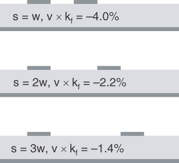
Figure 10-33 Simple rules of thumb for estimating the far-end cross talk for a pair of coupled 50-Ohm microstrips in FR4 for different spacings.
10.13 Decreasing Far-End Cross Talk
There are four general guidelines for decreasing far-end noise:
1. Increase the spacing between the signal traces. Increasing the spacing from 1 × w to 3 × w will decrease the far-end noise by 65%. Of course, the interconnect density will also decrease and may make the board more expensive.
2. Decrease the coupling length. The amount of far-end noise will scale with the coupling length. While v × kf can be as large as 4% for the tightest spacing (i.e., equal to the line width), if the coupled length can be kept very short, the magnitude of the far-end noise can be kept small. For example, if the rise time is 0.5 nsec, and the coupling length time delay, TD, is less than 0.1 nsec, the far-end noise can be kept below 4% × 0.1/0.5 = 0.8%. A TD of 0.1 nsec is a length of about 0.6 inch. A tightly coupled region under a BGA or connector field, for example, may be acceptable if it is kept short. The maximum co-parallel run length is a term that can typically be set up in the constraint file of a layout tool.
3. Add dielectric material to the top of the surface traces. When surface traces are required and the coupling length cannot be decreased, it is possible to decrease the far-end noise by adding a dielectric coating on top of the traces. This could be with a thicker solder mask, for example. Figure 10-34 shows how v × kf varies with the thickness of a top coat, assuming that a dielectric constant the same as the FR4, or 4, and assuming that the trace-to-trace separation is equal to the line width.

Figure 10-34 Variation of v × kf as the coating thickness above the signal lines increases. The bus uses tightly coupled 50-Ohm microstrip traces with 5-mil-line and 5-mil spacing in FR4, assuming a dielectric coating with the same dielectric constant. Simulated with Ansoft’s SI2D.
Adding dielectric above the trace will also increase the near-end noise and decrease the characteristic impedance of the traces. These have to be taken into account when adding a top coating.
As the coating thickness is increased, the far-end noise initially decreases and actually passes through zero. Then it goes positive and finally drops back and approaches zero. In a fully embedded microstrip, the dielectric is homogeneous, and there is no far-end noise. This is when the dielectric thickness is roughly five times the line width. This complex behavior is due to the precise shape of the fringe fields between the traces and also between the traces and the return plane, as well as to how they penetrate into the dielectric material as the coating thickness is increased.
It is possible to find a value of the coating thickness so the far-end noise for surface traces is exactly zero. In this particular case, it is with a thickness equal to the dielectric thickness between the traces and the return path, or about 3 mils.
TIP
In general, the optimum coating thickness will depend on all the geometry features and dielectric constants. Even a thin solder-mask coating will provide some benefit by decreasing the far-end noise a small amount.
4. Route the sensitive lines in stripline. Coupled lines in buried layers, as stripline cross sections, will have minimal far-end noise. If far end is a problem, the surest way of minimizing it is to route the sensitive lines in stripline.
In practice, it is usually not possible to use a perfectly homogenous dielectric material even in a stripline. There will always be some variations in the dielectric constant due to combinations of core and prepreg materials. Usually, the prepreg is resin rich and has a lower dielectric constant than the core laminate. This will give rise to an inhomogeneous dielectric distribution and some far-end noise.
Far-end noise can be the dominant source of noise in microstrip lines. These are the surface traces. When the spacing equals the line width, and the rise time is 1 nsec, the far-end noise will be more than 8% on a victim line in the middle of a bus with a coupling length longer than 6 inches. As the rise time decreases or coupling length increases, the far-end cross talk will increase. This is why far-end noise can often be the dominant problem in low-cost boards where many of the signal lines are routed as microstrip.
Whenever you use microstrip traces, a small warning should go off that there is the potential for too much far-end noise, and an estimate should be performed of the expected far-end noise to have confidence it won’t be a problem. If it is likely to be problematic, increase the routing pitch, decrease the coupling length, add some more solder mask, or route the long lines in stripline.
10.14 Simulating Cross Talk
In the special case of two uniform transmission lines with perfect terminations on each end, the expected voltage noise on the near and far ends can be calculated given the cross-section geometry and material properties. A 2D field solver will allow the calculation of kb and NEXT. The 2D field solver will also calculate kf, and from the TD of the coupled length and the rise time, we can get the FEXT.
But what if the termination changes, and what if the coupled length is just part of a larger circuit? This requires a circuit simulator that includes a model for a coupled transmission line. If the mutual capacitance per length and mutual inductance per length are known, an n-section coupled-transmission-line model can be created to allow the simulation for any termination strategy, provided that enough sections are used. The difficulty with an n-section lumped-circuit model is its complexity and computation time.
For example, if the time delay is 1 nsec, as in a 6-inch-long interconnect, and the required model bandwidth is 1 GHz, a total of 10 × 1 GHz × 1 nsec = 10 lumped-circuit sections would be required in the coupled model. For longer lengths, even more sections are required.
There is a class of simulators that allow the creation of coupled transmission lines using an ideal, distributed, coupled transmission-line model. These tools usually have an integrated 2D field solver. The geometry of the cross section is input, and the distributed coupled model is automatically created. The details of an ideal, distributed, coupled transmission line, often called an ideal differential pair, are reviewed in Chapter 11.
TIP
Coupled transmission-line circuits with arbitrary drivers, loads, and terminations can be simulated with a tool that has an integrated 2D field solver and allows automatic generation of a distributed, coupled transmission-line model from the cross-sectional information. These tools are incredibly powerful in predicting the performance of coupled noise in real systems.
Figure 10-35 shows an example of the near- and far-end noise predicted in an ideal case, with a low-impedance driver on an active line and terminating resistors on all the ends. The geometry in this case is closely coupled, 50-Ohm microstrips, with 5-mil-wide traces and 5-mil-wide spacing.

Figure 10-35 Simulating coupled transmission-line circuits with Mentor Graphics HyperLynx, showing the cross section of a tightly coupled pair of microstrip lines, the resulting circuit with the coupled lines with drivers and terminating resistors, and the simulated voltages on the active and quiet lines.
When source-series termination is used, the results are slightly more complicated. Figure 10-36 shows the circuit for source-series termination. In this case, the noise at the far end of the quiet line is important as this is the location of the receiver that would be sensitive to any noise. The actual noise appearing at the receiver end of the quiet line is subtle.

Figure 10-36 Circuit schematic for a source-series pair of coupled lines using Mentor Graphics HyperLynx.
Initially, the noise at the receiver end of the quiet line is due to the far-end noise from the active signal. This is a large negative spike. However, as the signal on the active line reflects off the open end of the receiver on the active line, it travels back to the source of the active line. As it travels back to the source, the receiver on the quiet line is now the backward end for this reflected signal wave. There will be backward noise on the quiet line at the receiver. Even though the receiver on the quiet line is at the far end of the quiet line, it will see both far-end and near-end noise because of the reflections of the signal in the active line.
The near-end noise on the quiet-line receiver is about the same as what is expected based on the ideal NEXT. Figure 10-37 shows the comparison of the ideal case of NEXT and FEXT in the quiet line, with the noise at the receiver on the quiet line for this source-series-terminated topology. This illustrates that the NEXT and FEXT terms are actually good figures of merit for the expected noise on the quiet line. Of course, the parasitics associated with the package models and the discrete termination components will complicate the received noise compared with the ideal NEXT and FEXT. A simulator tool will automatically take these details into account.

Figure 10-37 Simulated NEXT and FEXT in a far-end-terminated circuit compared with the receiver noise on the quiet line of a similar pair of lines but with source-series termination. Simulated with Mentor Graphics HyperLynx.
However, this is the case of having just one aggressor line coupling to the victim line. In a bus, there will be multiple traces coupling to a victim line. Each of the aggressor lines can add additional noise to the victim line. How many aggressors on either side should be included? The only way to know is to put in the numbers from a calculation.
In Figure 10-38, a bus circuit is set up, with one victim line and five aggressor lines on either side. Each line is configured with a source-series termination and receivers on the far ends. In this example, aggressive design rules are used for 50-Ohm striplines with 5-mil-wide traces and 5-mil spaces. The speed of a signal in this transmission line is about 6 inches/nsec. The signal has a rise time of about 1 nsec and a clock frequency of 100 MHz. The saturation length is ½ nsec × 6 inches/nsec = 3 inches. We use a length of 10 inches so the near-end noise will be saturated and thus a worst case.

Figure 10-38 Circuit diagram used to simulate the noise on a victim line when it is surrounded by five aggressor lines on each side. Each line has source-series termination, 5-mil-wide line, 5-mil space, 10-inch length, as 50-Ohm striplines in FR4. Simulation set up by Mentor Graphics HyperLynx.
There will be no far-end noise in this stripline. However, the signal reflecting off the far end of the aggressor lines will change direction, and its backward noise will appear at the victim’s far end. The signal in each aggressor is 3.3 volts.
Figure 10-39 shows the simulated noise at the receiver of the victim line. With just one of the adjacent lines switching, the noise on the quiet line is 195 mV. This is about 6%, probably too large all by itself for any reasonable noise budget. This geometry really is a worst case.

Figure 10-39 Simulated noise at the receiver of the victim line under the case of 1 aggressor, 2 aggressors, 4 aggressors, and 10 aggressors switching. Most of the noise is taken into account by including just the nearest two aggressors. Simulated with Mentor Graphics HyperLynx.
With the second aggressor on the other side of the victim line also switching, the noise is about twice, or 390 mV. This is 12% voltage noise from the adjacent two aggressor lines, one on either side of the victim line. Obviously, we get the same contribution of noise from each aggressor, and its noise contribution to the victim line just adds.
In stripline, the coupled noise drops off rapidly as the trace separation increases. We would expect the noise from the next two distant aggressor traces to be very small compared with the immediately adjacent traces. With the four nearest aggressors switching, the amount of noise at the receiver of the victim line is 410 mV, or 12.4%. Finally, the worst case is when all the aggressor lines switch. The noise is still 410 mV, indistinguishable from the noise with just the adjacent four nearest aggressors switching.
We see that the absolute worst-case noise in the bus is about 2.1 times the basic NEXT noise level. If we take into account only the adjacent traces switching, we would still be including about 95% of the total amount of noise, given this worst-case geometry. By including the switching from the two adjacent aggressor lines on both sides, we are including 100% of the coupled noise.
TIP
Using just the noise from the adjacent traces on either side of a victim line in cross-talk analysis is usually sufficient for most system-level simulations. This will account for 95% of the cross talk in a closely coupled bus.
In this example, very aggressive design rules were used. The amount of cross talk, 12%, is far above any reasonable noise budget. If, instead, the spacing equals two times the line width, the amount of noise from just one adjacent trace switching would be 1.5%. The noise from two adjacent traces switching would be 3%. When the four nearest aggressor traces switch, the coupled noise at the receiver of the quiet line would still be only 3%. It is not affected to any greater degree if all 10 adjacent traces switch. The same simulation, using this practical design rule of 5-mil-line width and 10-mil spacing, is shown in Figure 10-40.

Figure 10-40 Noise on the receiver of a central trace in a bus composed of 11 50-Ohm striplines in FR4 with 5-mil-wide traces and 10-mil spacings. The number of active traces switching is changed from just 1 to 2 to 4 and then all 10. Simulated using Mentor Graphics HyperLynx.
It is only necessary to look at the adjacent trace on either side of the victim line for a worst-case analysis.
TIP
When the most aggressive design rules are used (i.e., a spacing equal to the line width), more than 95% of the noise on a victim line that is part of a bus is due to coupling from the two nearest aggressor traces, one on either side of the victim line. When conservative design rules are used and the spacing is twice the line width, virtually all of the noise from the bus comes from coupling from the most adjacent aggressor on either side of the victim line.
This suggests that when establishing design rules for adequate spacings for long, parallel signal buses, the worst-case noise we might expect to find is at most 2.1 times the basic NEXT values. If the noise budget allocates 5% the voltage swing for cross talk on any victim net, the actual amount of NEXT that we should allow between adjacent nets should be 5% ÷ 2.1, which is a NEXT value of about 2%. We can use this as the design goal in establishing a spec for the closest spacing allowed in either microstrip or stripline traces.
10.15 Guard Traces
One way to decrease cross talk is by spacing the traces farther apart. Keeping the spacing twice the line width will ensure that the worst-case cross talk is less than 5%. In some cases, especially mixed-signal cases, keeping the cross talk significantly less than 5% is important. For example, a sensitive rf receiver may need as much as –100-dB isolation from any digital signals. A noise level of –100 dB is less than 0.001% of the active signal appearing on the sensitive quiet line.
It is often suggested that using guard traces will significantly decrease cross talk. This is indeed the case—but only with the correct design and configuration. A much more effective way of isolating two traces is to keep them on separate layers with different return planes. This can offer the greatest isolation of any routing alternative. However, if it is essential to route an aggressor and a victim line on the same signal layers and adjacent, then guard traces can offer an alternative way of controlling the cross talk under specific conditions.
Guard traces are separate traces that are placed between the aggressor lines and the victim lines that we want to shield. Examples of the geometry of guard traces are shown in Figure 10-41. A guard trace should be as wide as will fit between the signal lines, consistent with the fabrication design rules for spacing. Guard traces can be used in both microstrip and stripline cross sections. The value of a guard trace in microstrip is not very great, as a simple example will illustrate.

Figure 10-41 Examples of cross sections of traces that incorporate guard traces. The guard trace is hatched; all other traces are signal traces.
If we stick to design rules which specify that the smallest allowable spacing is equal to the line width, then before we can even add a guard trace, we must increase the spacing between two traces to three times the line width just to fit a trace between the aggressor and victim lines. In this geometry, we will always have less than 2% worst-case noise on the victim line. We can evaluate the added benefit of a guard trace in microstrip structures by comparing three cases:
1. Two closely spaced microstrip lines, 5-mil trace width, 5-mil spacing
2. Increasing the spacing to the minimum spacing (15 mils) that will allow a guard trace to fit
3. Increased spacing of 15 mils and adding the guard trace in place
These three examples are illustrated in Figure 10-42.
Figure 10-42 Three different microstrip structures evaluated for noise at the receiver of the victim line.
In addition, we can evaluate different termination strategies for the guard trace. Should it be left open, terminated at the ends, or shorted at the ends?
Figure 10-43 compares the peak noise on the receiver of the quiet line for all of these alternatives. The noise seen on the receiver is the combination of the reflections of the signal on the active line and the near- and far-end noise on the quiet line and their reflections. Combined with these first-order effects are the second-order contributions from the parasitics of the packages and resistor elements.

Figure 10-43 Three different geometries tested and with the guard trace left open on the ends, shorted on the ends, and terminated on the ends. Simulated with Mentor Graphics HyperLynx.
The peak noise with the traces close together is 130 mV. This is about 4%. Simply by pulling the traces far enough apart to fit a guard trace, the noise is reduced to 39 mV, or 1.2%. This is almost a factor-of-four reduction and is almost always a low enough cross talk, except in very rare situations. When the guard trace is inserted but left open, floating, we see the noise on the quiet line actually increases a slight amount.
However, if the guard trace is terminated with 50-Ohm resistors on both ends, the noise is reduced to about 25 mV, or 0.75%. When the guard trace is shorted at the ends, the noise on the quiet line is reduced to 22 mV, or about 0.66%.
TIP
You will get the most benefit by increasing the spacing. The noise is reduced by a factor of four. By adding the guard trace and shorting it on both ends, the noise is reduced further by a factor of two. If left open on the ends, it will actually increase the cross talk.
TIP
The guard trace affects the electric- and magnetic-field lines between the aggressor line and the victim line, and it will always decrease both the capacitance- and inductance-matrix elements.
The reduction in magnitude of the off-diagonal matrix elements by a guard trace is purely related to the geometry. It is independent of how the guard trace is electrically connected to the return path. This would imply that a guard trace would always be beneficial. However, the guard trace will also act as another signal line. Noise will couple to the guard trace from the aggressor line. This noise on the guard trace can then couple over to the quiet line. The amount of noise generated on the guard trace that can couple to the quiet line will depend on how it is terminated.
If the guard trace is left open, the maximum amount of noise is generated on the guard trace. If it is terminated with 50 Ohms on each end, less noise appears. Figure 10-44 shows the noise at the far end of the guard trace under the same conditions as above, with 5-mil line width, 5-mil space, and 50-Ohm microstrips with a 3.3-v, 100-MHz signal on the active line using source-series termination. It is clear that there is more noise generated on the guard trace when the guard trace is left open at the ends. This extra noise will couple more noise to the quiet line, which is why a guard trace with open ends can sometimes create more noise on the victim line than if it were not there.

Figure 10-44 Noise at the end of a guard trace when it is open and when it is terminated. This noise will couple to the quiet line. Simulated with Mentor Graphics HyperLynx.
The biggest benefit of a guard trace is when the guard trace is shorted on the ends. As the signal moves down the aggressor line, it will still couple noise to the guard trace. The backward-moving noise on the guard trace will hit the short at the near end and reflect with a reflection coefficient of –1. This means that much of the near-end noise on the guard trace, moving in the backward direction, will be canceled out with the coincident, negative, reflected near-end noise traveling in the forward direction on the guard trace.
TIP
Shorting the end of the guard trace will eliminate any near-end noise that would appear along the guard trace.
There will still be the buildup of the forward-moving far-end noise on the guard trace. This noise will continue to grow until it hits the shorted far end of the guard trace. At this point, it will see a reflection coefficient of –1 and reflect back. At the very far end of the guard trace, the net noise will be zero since there is, after all, a short. But the reflected far-end noise will continue to travel back to the near end of the guard trace. If all we do is short the two ends of the guard trace, the far-end noise on the guard trace will continue to reflect between the two ends, acting as a potential noise source to the victim line that is supposed to be protected. If there were no losses in the guard trace, the far-end noise would continue to rattle around the guard trace, always acting as a low-level noise source to couple back onto the victim line.
TIP
We can minimize the amount of far-end noise generated on the guard trace by adding more shorting vias, distributed down the length of the guard trace. These vias will have no impact on the noise directly coupled from the aggressor line to the victim line. They will only suppress the noise voltage generated on the guard trace.
The spacing between the shorting vias on the guard trace affects the amount of voltage noise generated on the guard trace in two ways. The far-end noise on the guard trace will only build up in the region between the vias. The closer the spacing, the lower the maximum far-end noise voltage that can build up on the guard trace. The more vias, the lower the far-end noise on the guard trace. This will mean lower voltage noise available to couple to the victim line.
Figure 10-45 shows a comparison of the coupled noise on the victim line for two coupled, 10-inch-long microstrip traces with a guard trace between them, one simulation with 1 shorting via at each end of the guard trace and a second with 11 shorting vias, spaced at 1-inch intervals along the guard trace.

Figure 10-45 Comparing the noise on the victim line using a guard trace with only 2 shorting vias and one with 11 shorting vias. The signal is 3.3 v, with a 0.7-nsec rise time and a low clock frequency of 25 MHz, to show the effect of the noise in the guard trace with only shorting vias on its ends. The maximum noise on the victim line is 35 mV out of 3.3 v, or 1%. Simulated with Mentor Graphics HyperLynx.
The initial noise on the victim line is the same, regardless of the number of shorting vias. This noise is due to the direct coupled noise between the aggressor and victim lines. The amount of coupled noise is related to the reduction in the size of the matrix element due to the presence of the guard trace. By adding multiple vias, we limit the buildup of the noise on the guard trace, which eliminates the possibility of this additional noise coupling to the victim line.
The second role of multiple shorting vias is in generating a negative reflection of the far-end noise, which will cancel out the incident far-end noise. However, this will be canceled out only where the incident and reflected far-end noise overlaps. If the spacing between the shorting vias is shorter than the width of the far-end noise, which is the rise time, this effect will not occur.
As a rough rule of thumb, the shorting vias should be distributed along the guard trace so that there are at least three vias within the spatial extent of the signal rise time. This will guarantee overlap of far-end noise and its negative reflection, causing cancellation of noise voltage on the guard trace.
If the rise time is 1 nsec, the spatial extent is 1 nsec × 6 inches/nsec = 6 inches. The spacing between shorting vias should be 6 inches/3 = 2 inches. If the rise time were 0.7 nsec, as in the previous example, the spatial extent would be 6 inches/nsec × 0.7 nsec = 4.2 inches, and the optimum spacing between shorting vias would be 4.2 inches/3 = 1.4 inches. In the previous example, vias were placed every 1 inch. Placing them any closer together would have no impact on the noise coupled to the victim line.
Of course, the shorter the signal rise time, the closer the spacing for the shorting vias required for optimum isolation. There will always be a compromise between the cost of the vias and the number that should be added. This should be an issue only when high isolation is required. In practice, there will be only a small impact on the noise in the victim line as the number of shorting vias is increased.
However, when high isolation is important, the coupled-noise to the quiet line will be much less in stripline, and stripline should always be used. In stripline structures, there will be much less far-end noise and much less need for shorting vias distributed along the length of the guard trace.
A guard trace can be very effective at limiting the isolation in a stripline structure. Figure 10-46 is the calculated near-end cross talk between an aggressor and victim, for a 50-Ohm stripline pair, with and without a guard trace between the aggressor and victim lines. In this example, the spacing between the two lines was increased and the guard trace was made as wide as would fit, consistent with the design rule of the spacing always greater than 5 mils. The guard trace, in the stripline configuration, offers a very significant amount of isolation over a configuration with no guard trace. Even isolations as large as –160 dB can be achieved using a wide guard trace in stripline. With separations of 30 mils between the active and aggressor lines, the guard trace can reduce the amount of isolation by almost three orders of magnitude.

Figure 10-46 Near-end cross talk in stripline pairs, with and without a guard trace. The signal-line width is 5 mils, and each line is 50 Ohms in FR4. The guard-trace width is increased as the signal-trace separation is increased to maintain a 5-mil gap. The flattening of the near-end noise at about 10–9 is due to the numerical noise floor of the simulator. Simulated with Ansoft’s SI2D.
A guard trace shields more than just the electric fields. There will also be induced currents in the guard trace from the proximity of the signal currents in the adjacent active lines. Figure 10-47 shows the current distribution in an active trace, a guard trace, and a quiet trace, with 5-mil width and spacing. Current is driven only in the active line, yet there is induced current in the guard trace, comparable to the current density in the return planes.
Figure 10-47 Current distribution in the conductors when a 100-MHz signal is driven in the aggressor line and the guard trace is shorted to the return path. Lighter color is higher current density. Gray scale is a log scale. Simulated with Ansoft’s SI2D.
This induced current will be in the opposite direction of the current in the active line. The magnetic-field lines from the induced current in the guard trace will further act to cancel the stray magnetic-field lines from the active line at the location of the quiet line. Both the electric-field shielding and magnetic-field shielding effects are fully accounted for by a 2D field solver when calculating the new capacitance- and inductance-matrix elements for a collection of conductors when one or more are used as a guard trace.
10.16 Cross Talk and Dielectric Constant
Near-end noise is related to the sum of the relative capacitive and inductive coupling: C12/C11 + L12/L11. Of course, the inductive coupling is completely unaffected by the dielectric material around the conductors.
In a 50-Ohm stripline geometry with a uniform dielectric constant everywhere, if the dielectric constant of all surrounding materials were decreased, the capacitance between the signal and return paths, C11, would decrease. However, the fringe-field capacitance between the two signal lines, C12, would also decrease by the same amount. There would be no change to the cross talk in a stripline.
However, if the dielectric constant were decreased everywhere, the characteristic impedance would increase from 50 Ohms. One way to get back to 50 Ohms would be to decrease the dielectric thickness. If the dielectric thickness were decreased to reach 50 Ohms, the fringe field lines would more tightly couple to the return plane, they would extend less to adjacent traces, and cross talk would decrease.
In a very subtle way, a lowered dielectric constant will decrease cross talk—but only indirectly. The lower dielectric constant will allow a closer spacing between the signal and return paths for the same target impedance, which will cause the lower cross talk.
Figure 10-48 shows the characteristic impedance of a stripline trace as the plane-to-plane separation changes, for a line width of 5 mils for two different dielectric constants. If a design were to use a laminate with a dielectric constant of 4.5, such as FR4, and then switch to 3.5, such as with Polyimide, the plane-to-plane spacing to maintain 50 Ohms would have to decrease from 14 mils to 11.4 mils. If the spacing between the 5-mil traces were kept at 5 mils, the near-end cross talk would reduce from 7.5% to 5.2%. This is a reduction in near-end cross talk of 30%.

Figure 10-48 Variation in characteristic impedance for two dielectric materials in 5-mil-wide stripline traces as the total separation between the planes is changed. A lower dielectric constant allows closer spacing between the planes for the same impedance, which would result in lower cross talk. Simulated with Ansoft’s SI2D.
TIP
Using a lower-dielectric-constant material would either allow lower cross-talk for the same routing pitch or tighter routing pitch for the same cross-talk spec. This could result in a smaller board if it were limited by cross-talk design rules.
10.17 Cross Talk and Timing
The time delay, TD, of a signal line depends on the length of the interconnect and the speed of the signal in the line. The speed of the signal depends on the dielectric constant of the surrounding material. In principle, cross talk from adjacent aggressor lines should not affect the time delay on a victim line. After all, how could the signal on adjacent traces affect the speed of the signal on the victim line?
TIP
In stripline, cross talk from adjacent aggressor lines does not affect the time delay on a victim line. The speed of a signal on a victim line is completely independent of the signals appearing on any nearby aggressor lines, and there is no impact on timing from cross talk.
However, in microstrip traces, there is a subtle interaction between cross talk and timing. This is due to the combination of the asymmetry of the dielectric materials and the different fringe-electric fields between the signal lines, depending on the data pattern on the aggressor lines.
Consider three closely spaced, 10-inch-long microstrip signal lines, each 5 mils wide with 5-mil spacing. The outer two lines will be aggressor lines, and the center line will be a victim line. The time delay for the victim line when there is no signal on the active lines is about 1.6 nsec. This is shown in Figure 10-49.

Figure 10-49 Time delay of 1.6 nsec between the signal leaving the victim driver and when it reaches the receiver on the victim line, both aggressors off. Simulated with Mentor Graphics HyperLynx.
The time delay of the signal on the victim line will depend on the voltage pattern on the aggressor lines. When the aggressors are switching opposite to the victim line, the time delay is decreased. When the aggressor lines are switching with the same signal as the victim line, the time delay of the victim line is increased.
The relationship of the voltage pattern on the aggressor lines to the time delay of the signal on the victim line is illustrated in Figure 10-50. The simulated results are shown in Figure 10-51.When the aggressor lines are off, the field lines from the signal voltage on the victim line see a combination of the bulk-material dielectric constant and the air above the line. This effective dielectric constant determines the speed of the signal.

Figure 10-50 Three configurations for signals on the victim line and aggressor lines. The voltage pattern on the aggressors affects the time delay of the victim line.

Figure 10-51 Received signal on the victim line when aggressors switch in the same direction and opposite to the signal on the victim line. Simulated with Mentor Graphics HyperLynx.
When the aggressor lines are switching opposite from the signal on the victim line, there are large fields between the victim and aggressor traces, and many of these field lines are in air with a low dielectric constant. The effective dielectric constant the victim signal sees would have a larger fraction of air and would be reduced compared to if the aggressors were not switching. A lower effective dielectric constant would result in a faster speed and a shorter time delay for the signal on the victim line. This is illustrated in Figure 10-52.

Figure 10-52 Electric-field distribution around victim and aggressor lines when they switch opposite and then when they switch in the same direction. Simulated with Mentor Graphics HyperLynx.
When the aggressor lines are switching in the same direction as the victim line, each trace is at the same potential, and there are few field lines in the air; most of them are in the bulk material. This means the effective dielectric constant the victim line sees will be higher, dominated by the bulk-material value. This will increase the effective dielectric constant for the victim-line signal when the aggressor lines switch in the same direction. This will decrease the signal speed and increase the time delay of the victim signal.
It is as though when the aggressors are switching opposite to the victim line, the speed of the signal is increased and the time delay is decreased. When the aggressors are switching with the same voltage pattern as the victim line, the speed of the victim signal is decreased and the time delay increased.
This impact of cross talk on time delay will happen only in tightly coupled microstrip lines where there is significant overlap of the fringe fields. If the lines are far enough apart where the cross-talk voltage is not a problem, the fringe fields will not overlap, and the time delay of the victim line will be independent of how the other traces are switching. This effect is fully taken into account when simulating with a distributed, coupled, transmission-line model.
10.18 Switching Noise
So far, we have been discussing cross talk when the return path is a wide, continuous plane, as with most transmission lines on circuit boards. In this environment, there is near- and far-end noise, and all the coupling occurs between adjacent signal lines, and virtually no coupling occurs from farther-away traces.
When the return path is not a uniform plane, the inductive coupling will increase much more than the capacitive coupling, and the noise will be dominated by the loop mutual inductance. This usually occurs in small localized regions of the interconnect, such as in packages, connectors, or local regions of the board where the return path is interrupted by gaps.
When loop mutual inductance dominates, and it occurs in a small region, we can model the coupling with a single lumped mutual inductor. The noise generated in the quiet line by the mutual inductance arises only when there is a dI/dt in the active line, which is when the edge switches. For this reason, the noise created when mutual inductance dominates is sometimes called switching noise, or dI/dt noise, or delta I noise. Ground bounce, as discussed previously, is a form of switching noise for the special case when the loop mutual inductance is dominated by the total inductance of the common return lead. Whenever there are shared return paths, ground bounce will occur. As pointed out, there are three ways of reducing ground bounce:
1. Increase the number of return paths so the total dI/dt in each return path is reduced.
2. Increase the width and decrease the length of the return path so it has a minimum partial self-inductance.
3. Bring each signal path in proximity to its return path to increase their partial mutual inductance with the return path.
However, even if there is no shared return path, there can still be cross talk between two or more signal-/return-path loops when dominated by mutual inductance. Loop mutual inductance in connectors and packages can often be the limiting feature in their high-speed performance.
By using a simple model, we can estimate how much loop mutual inductance between two signal/return loops is too much. As a signal passes through one pair of pins in a connector (the active path), there is a sudden change in the current in the loop right at the wavefront. This changing current causes voltage noise to be induced in an adjacent, quiet loop due to the mutual inductance between the two loops.
The voltage noise that is induced in the quiet loop is approximated by:
where:
Vn = voltage noise in the quiet loop
Lm = loop mutual inductance between the active and quiet loops
Ia = current change in the active loop
Z0 = typical impedance the signal sees in the active and quiet loops
Va = signal voltage in the active loop
RT = rise time of the signal (i.e., how fast the current turns on)
The only term that is really influenced by the connector or package design is the loop mutual inductance between the loops. The impedance the signal sees, typically on the order of 50 Ohms, is part of the system specification, as are the rise time and signal voltage.
The magnitude of acceptable switching noise depends on the allocated noise in the noise budget. Depending on the negotiating skills of the engineer who is responsible for selecting the connector or IC package, the switching noise would probably have to be below about 5% to 10% of the signal swing.
TIP
A signal-integrity engineer who has good negotiating skills and knows how hard it might be to find a connector or package with low enough mutual inductance might push for a higher allowable mutual inductance spec, therefore forcing another part of the system to require a tighter spec.
If the maximum acceptable switching noise is specified, this will define a maximum allowable loop mutual inductance between an active net and a quiet net. The maximum allowable loop mutual inductance is:
where:
Lm = loop mutual inductance between the active and quiet loops
Vn = voltage noise in the quiet loop
Va = signal voltage in the active loop
RT = rise time of the signal, or how fast the current turns on
Z0 = typical impedance the signal sees in the active and quiet loops
As a starting place, we will use these values:
Vn/Va = 5%
Z0 = 50 Ohms
RT = 1 nsec
The maximum allowable loop mutual inductance in this example would be 2.5 nH. If the rise time were to decrease, more switching noise would be created by the dI/dt, and the loop mutual inductance would have to be decreased to keep the switching noise down.
TIP
This suggests a simple rule of thumb: To keep switching noise to an acceptable level between a pair of signal and return paths, the loop mutual inductance between them should be less than Lm < 2.5 nH × RT, with RT in nsec.
If the rise time were 0.5 nsec, the maximum allowable loop mutual inductance would be 1.2 nH. As rise times decrease, the maximum allowable mutual inductance will also decrease. This will make connector and package design more difficult. There are three primary geometrical features that decrease loop mutual inductance:
1. Loop length—The most important term that influences loop mutual inductance is the length of the loops. Decrease the length of the loops, and the mutual inductance will decrease. This is why the trend in packages and connectors is to make them as short as possible, such as with chip scale packages.
2. Spacing between the loops—Increase the spacing, and the loop mutual inductance will decrease. There are practical limits to how far apart signal- and return-path pairs can be placed, though.
3. Proximity of the signal to return path of each loop—The loop mutual inductance is related to the loop self-inductance of either loop. Decreasing the loop self-inductance of either loop will decrease the loop mutual inductance between them. Bringing the signal closer to the signal path of one loop will decrease its impedance. In general, switching noise will be decreased with lower-impedance signal paths. Of course, using a value that is too low will introduce a new set of problems related to impedance discontinuities.
This analysis has assumed that the switching noise is generated between just two adjacent signal paths. If there is significant coupling between two aggressor lines and the same quiet line, keeping the same total switching noise on the victim line would require half the mutual inductance between either pair. The more aggressor lines that couple to the same victim line, the lower the allowable loop mutual inductance.
If we know how much loop mutual inductance there is between signal pairs in a package or connector, we can use the approximation in Equation 10-26 to immediately estimate their shortest usable rise time or highest usable clock frequency. For example, if the loop mutual inductance were 2.5 nH and the shortest rise time before the switching noise were more than 5%, the signal swing would be 1 nsec if there was coupling between just the two signal and return paths.
TIP
This suggests a simple rule of thumb: The shortest usable rise time, in nsec, limited by switching noise is RT > Lm/2.5 nH. The highest usable clock frequency would be about 10 × 1/RT = 250 MHz/Lm. This assumes that the clock period is 10 × RT.
For example, if the loop mutual inductance between a pair of signal paths is 1 nH, the maximum operating clock frequency might be on the order of 250 MHz. Of course, if there were five aggressor pairs that could couple to a signal victim line, each with 1-nH loop mutual inductance, the highest operating clock frequency would be reduced to 250 MHz/5 = 50 MHz. This is why leaded packages, with typically 1 nH of loop mutual inductance between signal paths, have maximum clock operating frequencies in the 50-MHz range.
10.19 Summary of Reducing Cross Talk
Cross talk can never be completely eliminated; it can only be reduced. The general design features that will reduce cross talk include the following:
1. Increase the pitch of the signal traces.
2. Use planes for return paths.
3. Keep coupled lengths short.
4. Route on stripline layers.
5. Decrease the characteristic impedance of signal traces.
6. Use laminates with lower dielectric constants.
7. Do not share return pins in packages and connectors.
8. When high isolation between two signal lines is important, route them on different layers with different return planes.
9. Because guard traces have little value in microstrip traces, in stripline, use guard traces with shorting vias on the ends and throughout the length.
TIP
Unfortunately, the features that reduce cross talk also invariably increase system costs. It is critically important to be able to accurately predict the expected cross talk so that the right trade-offs can be established to achieve the lowest cost at acceptable cross talk.
For cross talk in uniform transmission lines, the right tool is a 2D field solver with an integrated circuit simulator. For nonuniform transmission-line sections, the right tool is a 3D field solver, either static (if the section can be approximated by a single-lumped section) or full wave (if it is electrically long). With a predictive tool, it will be possible to evaluate how large a bang can be expected for the buck it will cost to implement the feature.
10.20 The Bottom Line
1. Cross talk is related to the capacitive and inductive coupling between two or more signal and return loops. It can often be large enough to cause problems.
2. The lowest cross talk between adjacent signal lines is when their return paths are a wide plane. In this environment, the capacitive coupling is comparable to the inductive coupling, and both terms must be taken into account.
3. Since cross talk is primarily due to the coupling from fringe fields, the most important way of decreasing cross talk is to space the signal paths farther apart.
4. The noise signature will be different on the near end and far end of a quiet line adjacent to a signal path. The near-end noise is related to the sum of the capacitively and inductively coupled currents. The far-end noise is related to the difference between the capacitively and inductively coupled currents.
5. To keep the near-end noise below 5% for the worst-case coupling in a bus, the separation should be at least two times the line width for 50-Ohm lines.
6. Near-end noise will reach a maximum value when the coupling length equals half the spatial extent of the rise time.
7. Far-end noise will scale with the ratio of the time delay of the coupling length to the rise time. For a pair of microstrip traces with a spacing equal to their line width, there will be 4% far-end noise when the time delay of the coupling length equals the rise time.
8. In a tightly coupled bus, 95% of the coupled noise can be accounted for by considering just the nearest aggressor line on either side of the victim line.
9. There is no far-end cross talk in striplines.
10. For very high isolation, signal lines should be routed on different layers with different return planes. If they have to be on the same layer and adjacent, use stripline with guard traces. Isolation greater than –160 dB is possible. In this case, watch out for ground bounce cross talk when signals change reference layers through vias.
11. Mutual inductance will dominate the coupled noise in some packages and connectors. As rise times decrease, the maximum amount of allowable mutual inductance between signal- and return-path loops must decrease. This will make it harder to design high-performance components.
End-of-Chapter Review Questions
10.1 In most typical digital systems, how much cross-talk noise on a victim line is too much?
10.2 If the signal swing is 5 V, how many mV of cross talk is acceptable?
10.3 If the signal swing is 1.2 V, how many mV of cross talk is acceptable?
10.4 What is the fundamental root cause of cross talk?
10.5 What is superposition, and how does this principle help with cross-talk analysis?
10.6 In a mixed signal system, how much isolation might be required?
10.7 What are the two root causes of cross talk?
10.8 What elements are in the equivalent circuit model for coupling?
10.9 If the rise time of a signal is 0.5 nsec, and the coupled length is 12 inches, how many sections would be needed in an n-section LC model?
10.10 What are two ways of reducing the extent of the fringe electric and magnetic fields?
10.11 Why is the total current transferred between the active line and the quiet line independent of the rise time of the signal?
10.12 What is the signature of near-end noise?
10.13 What is the signature of far-end noise in microstrip?
10.14 What is the signature of far-end noise in stripline?
10.15 What is the typical near-end cross-talk coefficient for a tightly coupled pair of striplines?
10.16 When the far end of the quiet line is open, what is the noise signature on the near end of the quiet line of two coupled microstrips?
10.17 When a positive edge is the signal on the active line, the near-end signature is a positive signal. What is the noise signature when the active signal is a negative signal? What is the noise signature for a square pulse as the active signal?
10.18 Why are the off-diagonal Maxwell capacitance matrix elements negative?
10.19 If the rise time of a signal is 0.2 nsec, what is the saturation length in an FR4 interconnect for near-end cross talk?
10.20 In a stripline, which contributes more near-end cross talk: capacitively induced current or inductively induced current?
10.21 How does the near-end noise scale with length and rise time?
10.22 How does the far-end cross talk in microstrip scale with length and rise time?
10.23 Why is there no far-end noise in stripline?
10.24 What are three design features to adjust to reduce near-end crosstalk?
10.25 What are three design features to adjust to reduce far-end cross talk?
10.26 Why does lower dielectric constant reduce cross talk?
10.27 If a guard trace were to be added between two signal lines, how far apart would the signal lines have to be moved? What would the near-end cross talk be if the traces were moved apart and no guard trace were added? What applications require a lower cross talk than this?
10.28 If really high isolation is required, what geometry offers the highest isolation with guard traces? How should the guard trace be terminated?
10.29 What is the root cause of ground bounce?
10.30 List three design features to reduce ground bounce.