
The microprocessor—a consolidation of all the components of a central processing unit (CPU) of a computer on a single chip of silicon—was born in 1971. It was a modest beginning: The first microprocessor, the Intel 4004, contained about 2300 transistors. Today, nearly three decades later, microprocessors made for home computers are approaching the 10,000,000 transistor mark.
Yet what the microprocessor actually does on a fundamental level has remained unchanged. While those millions of additional transistors in today's chips might be doing interesting things, in an initial exploration of the microprocessor they offer more distraction than enlightenment. To obtain the clearest view of what a microprocessor does, let's look at the first ready-for-prime-time microprocessors.
These microprocessors appeared in 1974, the year in which Intel introduced the 8080 (pronounced eighty eighty) in April and Motorola—a company that had been making semiconductors and transistor-based products since the 1950s—introduced the 6800 (sixty-eight hundred) in August. These weren't the only microprocessors available that year. Also in 1974, Texas Instruments introduced the 4-bit TMS 1000, which was used in many calculators, toys, and appliances; and National Semiconductor introduced the PACE, which was the first 16-bit microprocessor. In retrospect, however, the 8080 and the 6800 were certainly the two most historically significant chips.
Intel set the initial price of the 8080 at $360, a sly dig at IBM's System/360, a large mainframe system used by many large corporations that cost millions. (Today you can buy an 8080 chip for $1.95.) It's not as if the 8080 is comparable to System/360 in any way, but within a few years IBM itself would certainly be taking notice of these very small computers.
The 8080 is an 8-bit microprocessor that contains about 6000 transistors, runs at a 2 MHz clock speed, and addresses 64 kilobytes of memory. The 6800 (also selling these days for $1.95) has about 4000 transistors and also addresses 64 KB of memory. The first 6800 ran at 1 MHz, but by 1977 Motorola introduced later versions running at 1.5 and 2 MHz.
These chips are referred to as single-chip microprocessors and less accurately as computers on a chip. The processor is only one part of the whole computer. In addition to the processor, a computer at the very least requires some random access memory (RAM), some way for a person to get information into the computer (an input device), some way for a person to get information out of the computer (an output device), and several other chips that bind everything together. But I'll describe these other components in greater detail in Chapter 21.
For now, let's look at the microprocessor itself. Often a description of a microprocessor is accompanied by a block diagram that illustrates the internal components of the microprocessor and how they're connected. But we had enough of that in Chapter 17. Instead, we'll get a sense of what's inside the processor by seeing how it interacts with the outside world. In other words, we can think of the microprocessor as a black box whose internal operations we don't need to study minutely in order to understand what it does. We can instead grasp what the microprocessor does by examining the chip's input and output signals, and in particular the chip's instruction set.
Both the 8080 and 6800 are 40-pin integrated circuits. The most common IC package for these chips is about 2 inches long, about a half inch wide, and ⅛ inch thick:
Of course, what you see is just the packaging. The actual wafer of silicon inside is much smaller—in the case of the early 8-bit microprocessors, the silicon is less than ¼ inch square. The packaging protects the silicon chip and also provides access to all of the chip's input and output points through the pins. The diagram on the following page shows the function of the 40 pins of the 8080.
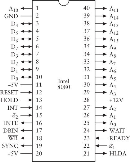
Every electrical or electronic device that we've built in this book has required some kind of electrical power supply. One of the 8080's quirks is that it requires three power supply voltages. Pin 20 must be connected to a 5-volt power supply, pin 11 to a –5-volt power supply, and pin 28 to a 12-volt power supply. You connect pin 2 to ground. (In 1976, Intel released the 8085 chip, which simplified these power requirements.)
All the remaining pins are drawn as arrows. An arrow from the chip indicates an output signal. This is a signal controlled by the microprocessor that other chips in the computer respond to. An arrow into the chip indicates an input signal. This is a signal that comes from another chip in the computer that the 8080 responds to. Some pins are both inputs and outputs.
The processor in Chapter 17 required an oscillator to make it go. The 8080 requires two different synchronized 2-MHz clock inputs labeled ø1 and ø2 on pins 22 and 15. These signals are most conveniently supplied by another chip made by Intel known as the 8224 Clock Signal Generator. You connect an 18-MHz quartz crystal to this chip, and it basically does the rest.
A microprocessor always has multiple output signals that address memory. The number of signals it has for this purpose is directly related to the amount of memory the microprocessor can address. The 8080 has 16 signals labeled A0 through A15, which give it the ability to address 216, or 65,536, bytes of memory.
The 8080 is an 8-bit microprocessor that reads data from memory and writes data to memory 8 bits at a time. The chip includes eight signals labeled D0 through D7. These signals are the only ones on the chip that are both inputs and outputs. When the microprocessor reads a byte of memory, the pins function as inputs; when the microprocessor writes a byte to memory, the pins function as outputs.
The other ten pins of the microprocessor are control signals. The RESET input, for example, is used to reset the microprocessor. The output signal ![]() indicates that the microprocessor needs to write a byte of memory into RAM. (The
indicates that the microprocessor needs to write a byte of memory into RAM. (The ![]() signal corresponds to the Write input of the RAM array.) In addition, other control signals appear on the D0 through D7 pins at a particular time while the chip reads instructions. Computer systems built around the 8080 generally use the 8228 System Controller chip to latch these additional control signals. I'll describe some control signals later on, but the 8080's control signals are notoriously messy, so unless you're going to actually design a computer based on the chip, it's best not to torture yourself with its control signals.
signal corresponds to the Write input of the RAM array.) In addition, other control signals appear on the D0 through D7 pins at a particular time while the chip reads instructions. Computer systems built around the 8080 generally use the 8228 System Controller chip to latch these additional control signals. I'll describe some control signals later on, but the 8080's control signals are notoriously messy, so unless you're going to actually design a computer based on the chip, it's best not to torture yourself with its control signals.
Let's assume that the 8080 microprocessor is connected to 64 KB of memory that we have the ability to write bytes into and read bytes from independent of the microprocessor.
After the 8080 chip is reset, it reads the byte located at memory address 0000h into the microprocessor. It does this by outputting 16 zeros on the address signals A0 through A15. The byte it reads should be an 8080 instruction, and the process of reading this byte is known as an instruction fetch.
In the computer we built in Chapter 17, all instructions (except HLT) were 3 bytes in length, consisting of an opcode and a 2-byte address. In the 8080, instructions can be 1 byte, 2 bytes, or 3 bytes in length. Some instructions cause the 8080 to read a byte from a particular location in memory into the microprocessor. Some instructions cause the 8080 to write a byte from the microprocessor into a particular location in memory. Other instructions cause the 8080 to do something internally without using any RAM. After processing the first instruction, the 8080 accesses the second instruction in memory, and so forth. Together, these instructions constitute a computer program that can do something interesting.
When the 8080 is running at its maximum speed of 2 MHz, each clock cycle is 500 nanoseconds. (1 ÷ 2,000,000 cycles per second = 0.000000500 seconds.) The instructions in the Chapter 17 computer all required 4 clock cycles. Each 8080 instruction requires anywhere from 4 to 18 clock cycles. This means that each instruction is executed in 2 to 9 microseconds (millionths of a second).
Probably the best way to understand what a particular microprocessor is capable of doing is to examine its complete instruction set in a systematic manner.
The final computer in Chapter 17 had only 12 instructions. An 8-bit microprocessor could easily have as many as 256 instructions, each opcode corresponding to a particular 8-bit value. (It could actually have more if some instructions have 2-byte opcodes.) The 8080 doesn't go quite that far, but it does have 244 opcodes. That might seem like a lot, but all in all, the 8080 doesn't really do all that much more than the computer in Chapter 17. For example, if you need to do multiplication or division using an 8080, you still need to write your own little program to do it.
As you'll recall from Chapter 17, each opcode in a processor's instruction set is usually associated with a particular mnemonic, and some of these mnemonics might have arguments. But these mnemonics are solely for convenience in referring to the opcodes. The processor reads only bytes; it knows nothing about the text that makes up the mnemonics. (For purposes of clarity, I've taken some liberty with the mnemonics as they appear in Intel's documentation of the 8080.)
The Chapter 17 computer had two important instructions that we initially called Load and Store. Each of these instructions occupied 3 bytes of memory. The first byte of a Load instruction was the opcode, and the 2 bytes that followed the opcode indicated a 16-bit address. The processor loaded the byte at that address into the accumulator. Similarly, the Store instruction saved the contents of the accumulator in the address indicated in the instruction.
Later on, we discovered that we could abbreviate these two opcodes using mnemonics:
LOD A,[aaaa]
STO [aaaa],A
where A stands for the accumulator (the destination in the Load instruction and the source in the Store instruction) and aaaa indicates a 16-bit memory address, usually written as 4 hexadecimal digits.
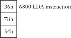
The 8-bit accumulator in the 8080 is called A, just like the accumulator in Chapter 17. And like the computer in Chapter 17, the 8080 includes two instructions that do exactly the same thing as the Load and Store instructions. The 8080 opcodes for these two instructions are 32h and 3Ah, and each opcode is followed by a 16-bit address. The 8080 mnemonics are STA (standing for Store Accumulator) and LDA (Load Accumulator):
Opcode | Instruction |
|---|---|
32 |
|
3A |
|
In addition to the accumulator, the 8080 contains six registers that can also hold 8-bit values inside the microprocessor. These registers are very similar to the accumulator; indeed, the accumulator is considered to be a special type of register. Like the accumulator, the other six registers are latches; the processor can move bytes from memory into registers, and from registers back into memory. The other registers, however, aren't as versatile as the accumulator. When you add two 8-bit numbers, for example, the result always goes into the accumulator rather than into one of the other registers.
The six additional registers in the 8080 are named B, C, D, E, H, and L. The first question people usually ask is, "What happened to F and G?" and the second question is, "And what about I, J, and K?" The answer is that registers H and L are so called because they're special in a certain way. H stands for high and L stands for low. Very often the 8-bit quantities in H and L are treated in tandem as a 16-bit register pair named HL, H being the high-order byte and L being the low-order byte. This 16-bit value is often used to address memory. We'll see how this works shortly.
Are all these registers necessary? Why didn't we need them in the Chapter 17 computer? In theory, they aren't necessary. But they turn out to be very convenient. Many computer programs juggle several numbers at the same time. It's easiest to do this if all the numbers are stored in microprocessor registers rather than memory. The program is usually faster as well: The fewer times a program needs to access memory, generally the faster it will run.
No fewer than 63 opcodes are devoted to a single 8080 instruction called MOV, which is short for Move. This instruction is just a single byte. The instruction usually moves the contents of one register into another (or the same) register. The large number of MOV instructions is a normal consequence of designing a microprocessor with seven registers (including the accumulator).
Here are the first 32 MOV instructions. Remember that the destination is the argument on the left and the source is the argument on the right:
Opcode | Instruction | Opcode | Instruction |
|---|---|---|---|
40 |
| 50 |
|
41 |
| 51 |
|
42 |
| 52 |
|
43 |
| 53 |
|
44 |
| 54 |
|
45 |
| 55 |
|
46 |
| 56 |
|
47 |
| 57 |
|
48 |
| 58 |
|
49 |
| 59 |
|
4A |
| 5A |
|
4B |
| 5B |
|
4C |
| 5C |
|
4D |
| 5D |
|
4E |
| 5E |
|
4F |
| 5F |
|
These are handy instructions to have. Whenever you have a value in one register, you know you can move it to another register. Notice also the four instructions that use the HL register pair, such as
MOV B,[HL]
The LDA instruction shown earlier transfers a byte from memory into the accumulator; the 16-bit address of the byte directly follows the LDA opcode. This MOV instruction transfers a byte from memory into register B. But the address of the byte to be loaded into the register is stored in the register pair HL registers. How did HL come to hold a 16-bit memory address? Well, it could happen in a variety of ways. Maybe the address was calculated in some way.
To summarize, these two instructions
LDA A,[aaaa]
MOV B,[HL]
both load a byte from memory into the microprocessor, but they use two different methods to address memory. The first method is called direct addressing and the second method is called indexed addressing.
The second batch of 32 MOV instructions shows that the memory location addressed by HL can also be a destination:
Opcode | Instruction | Opcode | Instruction |
|---|---|---|---|
40 |
| 50 |
|
60 |
| 70 |
|
61 |
| 71 |
|
62 |
| 72 |
|
63 |
| 73 |
|
64 |
| 74 |
|
65 |
| 75 |
|
66 |
| 76 |
|
67 |
| 77 |
|
68 |
| 78 |
|
69 |
| 79 |
|
6A |
| 7A |
|
6B |
| 7B |
|
6C |
| 7C |
|
6D |
| 7D |
|
6E |
| 7E |
|
6F |
| 7F |
|
Several of these instructions, such as
MOV A,A
don't do anything useful. But the instruction
MOV [HL],[HL]
doesn't exist. The opcode that would otherwise correspond to that instruction is actually a HLT (Halt) instruction.
A more revealing way to look at all these MOV opcodes is to examine the bit pattern of the opcode. The MOV opcode consists of the 8 bits
01dddsss
in which the letters ddd represent a 3-bit code that refers to a destination, and sss is a 3-bit code that refers to a source. These 3-bit codes are
| 000 = Register B |
| 001 = Register C |
| 010 = Register D |
| 011 = Register E |
| 100 = Register H |
| 101 = Register L |
| 110 = Contents of memory at address HL |
| 111 = Accumulator |
For example, the instruction
MOV L,E
is associated with the opcode
| 01101011 |
or 6Bh. You can check the preceding table to verify that.
So probably somewhere inside the 8080, the 3 bits labeled sss are used in a 8-Line-to-1-Line Data Selector, and the 3 bits labeled ddd are used to control a 3-Line-to-8-Line Decoder that determines which register latches a value.
It's also possible to use registers B and C as a 16-bit register pair BC, and registers D and E as a 16-bit register pair DE. If either register pair contains the address of a memory location that you want to use to load or store a byte, you can use the following instructions:
Opcode | Instruction | Opcode | Instruction |
|---|---|---|---|
02 |
| 0A |
|
12 |
| 1A |
|
Another type of Move instruction is called Move Immediate and is assigned the mnemonic MVI. The Move Immediate instruction is composed of 2 bytes. The first is the opcode, and the second is a byte of data. That byte is transferred from memory into one of the registers or to the memory location addressed by the HL register pair:
Opcode | Instruction |
|---|---|
06 |
|
0E |
|
16 |
|
1E |
|
26 |
|
2E |
|
36 |
|
3E |
|
For example, after the instruction
MVI E,37h
the register E contains the byte 37h. This is considered to be a third method of addressing memory, called immediate addressing.
A collection of 32 opcodes do the four basic arithmetical operations we're familiar with from the processor we developed in Chapter 17. These are addition (ADD), addition with carry (ADC), subtraction (SUB), and subtraction with borrow (SBB). In all cases, the accumulator is one of the two operands and is also the destination for the result:
Opcode | Instruction | Opcode | Instruction |
|---|---|---|---|
80 |
| 90 |
|
81 |
| 91 |
|
82 |
| 92 |
|
83 |
| 93 |
|
84 |
| 94 |
|
85 |
| 95 |
|
86 |
| 96 |
|
87 |
| 97 |
|
88 |
| 98 |
|
89 |
| 99 |
|
8A |
| 9A |
|
8B |
| 9B |
|
8C |
| 9C |
|
8D |
| 9D |
|
8E |
| 9E |
|
8F |
| 9F |
|
Suppose A contains the byte 35h and register B contains the byte 22h. After executing
SUB A,B
the accumulator contains the byte 13h.
If A contains the byte 35h, and register H contains the byte 10h, and L contains the byte 7Ch, and the memory location 107Ch contains the byte 4Ah, the instruction
ADD A,[HL]
adds the byte in the accumulator (35h) and the byte addressed by the register pair HL (4Ah) and stores the result (7Fh) in the accumulator.
The ADC and SBB instructions allow the 8080 to add and subtract 16-bit, 24-bit, 32-bit, and larger numbers. For example, suppose the register pairs BC and DE both contain 16-bit numbers. You want to add them and put the result in BC. Here's how to do it:
MOV A,C     ; Low-order byte
ADD A,E
MOV C,A
MOV A,B     ; High-order byte
ADC A,D
MOV B,A
The two addition instructions are ADD for the low-order byte and ADC for the high-order byte. Any carry bit that results from the first addition is included in the second addition. But because you can add only with the accumulator, this little snippet of code requires no fewer than 4 MOV instructions. Lots of MOV instructions usually show up in 8080 code.
This is a good time to talk about the 8080 flags. In our processor in Chapter 17, we had a Carry flag and a Zero flag. The 8080 has three more, called Sign, Parity, and Auxiliary Carry. All the flags are stored in yet another 8-bit register called the Program Status Word (PSW). Instructions such as LDA, STA, or MOV don't affect the flags at all. The ADD, SUB, ADC, and SBB instructions do affect the flags, however, in the following way:
The Sign flag is set to 1 if the most significant bit of the result is 1, meaning that the result is negative.
The Zero flag is set to 1 if the result is 0.
The Parity flag is set to 1 if the result has even parity, which means that the number of 1 bits in the result is even. The parity flag is 0 if the result has odd parity. Parity is sometimes used as a crude form of error checking. This flag isn't often used in 8080 programming.
The Carry flag is set to 1 if an ADD or ADC operation results in a carry or if a SUB and SBB does not result in a carry. (This is different from the implementation of the Carry flag in the Chapter 17 computer.)
The Auxiliary Carry flag is 1 if the operation results in a carry from the low nibble into the high nibble. This flag is used only for the DAA (Decimal Adjust Accumulator) instruction.
Two instructions affect the carry flag directly:
Opcode | Instruction | Meaning |
|---|---|---|
37 |
| Set Carry flag to 1 |
3F |
| Complement Carry flag |
The computer in Chapter 17 performed ADD, ADC, SUB, and SBB instructions (although not with nearly as much flexibility), but the 8080 does Boolean AND, OR, and XOR operations as well. Both arithmetic and logical operations are performed by the processor's Arithmetic Logic Unit (ALU).
Opcode | Instruction | Opcode | Instruction |
|---|---|---|---|
A0 |
| B0 |
|
A1 |
| B1 |
|
A2 |
| B2 |
|
A3 |
| B3 |
|
A4 |
| B4 |
|
A5 |
| B5 |
|
A6 |
| B6 |
|
A7 |
| B7 |
|
A8 |
| B8 |
|
A9 |
| B9 |
|
AA |
| BA |
|
AB |
| BB |
|
AC |
| BC |
|
AD |
| BD |
|
AE |
| BE |
|
AF |
| BF |
|
The AND, XOR, and OR instructions perform bitwise operations. This means that the logical operation is performed on each pair of bits separately.
For example,
MVI A,0Fh
MVI B,55h
AND A,B
The value in the accumulator will be 05h. If the third instruction were an OR, the result would be 5Fh. If the instruction were an XOR, the result would be 5Ah.
The CMP (Compare) instruction is just like the SUB instruction except that the result isn't stored in the accumulator. In other words, the CMP performs a subtraction and then throws away the result. What's the point? The flags! The flags tell you the relationship between the 2 bytes that you compared. For example, consider the following instructions:
MVI B,25h
CMP A,B
After this instruction, the contents of A remain unchanged. However, the Zero flag is set if the value in A equals 25h. The Carry flag is set if the value in A is less than 25h.
The eight arithmetic and logic operations also have versions that operate on an immediate byte:
Opcode | Instruction | Opcode | Instruction |
|---|---|---|---|
C6 |
| E6 |
|
CE |
| EE |
|
D6 |
| F6 |
|
DE |
| FE |
|
For example, the two lines shown above can be replaced with
CPI A,25h
Here are two miscellaneous 8080 instructions:
Opcode | Instruction |
|---|---|
27 |
|
2F |
|
CMA stands for Complement Accumulator. It performs a ones' complement of the value in the accumulator. Every 0 becomes a 1 and every 1 becomes a 0. If the accumulator is 01100101, the CMA instruction causes it to be 10011010. You can also complement the accumulator using the instruction
XRI A,FFh
DAA stands for Decimal Adjust Accumulator, as I mentioned earlier, and it's probably the most sophisticated single instruction in the 8080. A whole little section of the microprocessor is dedicated specifically to performing this instruction.
The DAA instruction helps a programmer implement decimal arithmetic using a method of representing numbers known as binary-coded decimal, or BCD. In BCD, each nibble of data may range only from 0000 through 1001, corresponding to decimal digits 0 through 9. The 8 bits of a byte can store two decimal digits in BCD format.
Suppose the accumulator contains the BCD value 27h. Because this is a BCD value, it actually refers to the decimal value 27. (Normally, the hexadecimal value 27h has the decimal equivalent 39.) Suppose also that register B contains the BCD value 94h. If you execute the instruction
MVI A,27h
MVI B,94h
ADD A,B
the accumulator will contain the value BBh, which, of course, isn't a BCD value because the nibbles of BCD bytes never exceed 9. But now execute the instruction
DAA
Now the accumulator contains 21h, and the Carry flag is set. That's because the decimal sum of 27 and 94 equals 121. This can be handy if you need to do BCD arithmetic.
Very often it's necessary to add 1 to a particular value or subtract 1 from a value. In the multiplication program in Chapter 17, we needed to subtract 1 from a value, and the way we did it was to add FFh, which is the two's complement value of –1. The 8080 includes special instructions for increasing a register or memory location by 1 (this is known as an increment) or decreasing by 1 (decrement):
Opcode | Instruction | Opcode | Instruction |
|---|---|---|---|
04 |
| 05 |
|
0C |
| 0D |
|
14 |
| 15 |
|
1C |
| 1D |
|
24 |
| 25 |
|
2C |
| 2D |
|
34 |
| 35 |
|
3C |
| 3D |
|
The single-byte INR and DCR instructions affect all flags except the Carry flag.
The 8080 also includes four Rotate instructions. These instructions shift the contents of the accumulator 1 bit to the left or right:
Opcode | Instruction | Meaning |
|---|---|---|
07 |
| Rotate accumulator left |
0F |
| Rotate accumulator right |
17 |
| Rotate accumulator left through carry |
1F |
| Rotate accumulator right through carry |
Only the Carry flag is affected by these instructions.
Suppose the accumulator contains the value A7h, or 10100111 in binary. The RLC instruction shifts the bits left. The lowest bit (shifted out of the bottom) becomes the highest bit (shifted into the top) and also determines the state of the Carry flag. The result is 01001111, and the Carry flag is 1. The RRC instruction shifts the bits right in the same way. Beginning with 10100111, the result after an RRC instruction is 11010011, and the Carry flag is 1.
The RAL and RAR instructions work a little differently. The RAL instruction sets the Carry flag to the lowest bit of the accumulator when shifting left but sets the highest bit to the previous contents of the Carry flag. For example, if the accumulator contains 10100111 and the Carry flag is 0, RAL causes the accumulator to become 01001110 and the Carry flag to be 1. Similarly, under the same initial conditions RAR causes the accumulator to become 01010011 and the Carry flag to be set to 1.
The shift instructions come in handy when you're multiplying a number by 2 (that's a shift left) or dividing a number by 2 (a shift right).
The memory that the microprocessor addresses is called random access memory (RAM) for a reason: The microprocessor can access any particular memory location simply by supplying an address of that location. RAM is like a book that we can open to any page. It's not like a week's worth of a newspaper on microfilm. Finding something in Saturday's edition requires us to scan through most of the week. Similarly, playing the last song on a cassette tape requires us to fast forward through the whole side of the album. The term for microfilm or tape storage isn't random access but sequential access.
Random access memory is definitely a good thing, particularly for microprocessors, but sometimes it's advantageous to treat memory a little differently. Here's a form of storage that's neither random nor sequential: Suppose you work in an office where people come to your desk to give you jobs to do. Each job involves a file folder of some sort. Often when you're working on one job, you find that before you can continue you must do a related job using another file folder. So you leave the first folder on your desk and put the second one on top of it to work on that. Now someone comes to your desk to give you yet another job that has higher priority than the earlier one. You're handed a new file folder and you work with that one on top of the other two. That job requires yet another file folder, and soon you have a pile of four file folders on your desk.
Notice that this pile is actually a very orderly way to store and keep track of all the jobs you're doing. The topmost file folder always has the highest-priority job. After you get rid of that one, the next one on the pile must be attended to, and so on. When you finally get rid of the last file folder on your desk (the first one you started with), you can go home.
The technical term for this form of storage is a stack. You're stacking things from the bottom up and removing them from the top down. It's also called last-in-first-out storage, or LIFO. The last thing put on the stack is the first thing taken off the stack. The first thing put on the stack is the last thing taken off the stack.
Computers also can use a stack, not for storing jobs but for storing numbers, and it's something that turns out to be quite convenient. Putting something on the stack is called a push, and taking something off the stack is called a pop.
Suppose you were writing an assembly-language program that used registers A, B, and C. But you notice that you've reached a point where the program needs to do something else—another little calculation that also needs to use registers A, B, and C. You eventually want to come back to what you were doing before, however, and continue using A, B, and C with the values they previously had.
What you could do, of course, is simply store registers A, B, and C in various locations in memory and later load these locations back into the registers. But that requires keeping track of where you stored them. A much cleaner way to do it is to push the registers on the stack:
PUSH A
PUSH B
PUSH C
I'll explain what these instructions actually do in a moment. For now, all we need to know is that they somehow save the contents of the registers in last-in-first-out memory. Once these statements are executed, your program can use these registers for other purposes without worry. To get the earlier values back, you simply pop them from the stack in the reverse order, as shown at the top of the following page.
POP C
POP B
POP A
Remember: Last in, first out. Accidentally switching around these POP statements would constitute a bug.
What's particularly nice about the stack mechanism is that lots of different sections of a program can use the stack without causing problems. For example, after the program pushes A, B, and C on the stack, another section of the program could decide it needs to do the same thing with registers C, D, and E:
PUSH C
PUSH D
PUSH E
Then all that's necessary is for that section of the program to restore the registers this way:
POP E
POP D
POP C
before the first section popped C, B, and A.
How is the stack implemented? The stack is, first of all, just a section of normal RAM that isn't being used for anything else. The 8080 microprocessor contains a special 16-bit register that addresses this section of memory. That 16-bit register is called the Stack Pointer.
My examples of pushing and popping individual registers weren't quite accurate for the 8080. The 8080 PUSH instruction actually stores 16-bit values on the stack, and the POP instruction retrieves them. So instead of instructions like PUSH C and POP C, we have the following 8 instructions:
Opcode | Instruction | Opcode | Instruction |
|---|---|---|---|
C5 |
| C1 |
|
D5 |
| D1 |
|
E5 |
| E1 |
|
F5 |
| F1 |
|
The PUSH BC instruction stores registers B and C on the stack, and POP BC retrieves them. The abbreviation PSW in the last row refers to the Program Status Word, which, as you'll recall, is the 8-bit register that contains the flags. The two instructions in the bottom row actually push and pop both the accumulator and the PSW. If you want to save the contents of all the registers and flags, you can use
PUSH PSW
PUSH BC
PUSH DE
PUSH HL
When you later need to restore the contents of these registers, use the POP instructions in reverse order:
POP HL
POP DE
POP BC
POP PSW
How does the stack work? Let's assume the Stack Pointer is 8000h. The PUSH BC instruction causes the following to occur:
The Stack Pointer is decremented to 7FFFh.
The contents of register B are stored at the Stack Pointer address, or 7FFFh.
The Stack Pointer is decremented to 7FFEh.
The contents of register C are stored at the Stack Pointer address, or 7FFEh.
A POP BC instruction executed when the Stack Pointer is still 7FFEh undoes everything:
The contents of register C are loaded from the Stack Pointer address, or 7FFEh.
The Stack Pointer is incremented to 7FFFh.
The contents of register B are loaded from the Stack Pointer address, or 7FFFh.
The Stack Pointer is incremented to 8000h.
For every PUSH instruction, the stack increases 2 bytes in size. It's possible—possibly due to a bug in a program—that the stack will get so big that it will begin to overwrite some code or data needed by a program. This is a problem known as stack overflow. Similarly, too many POP instructions can prematurely exhaust the contents of the stack, a condition known as stack underflow.
If you have 64 KB of memory connected to your 8080, you might want to initially set the Stack Pointer to 0000h. The first PUSH instruction decrements that address to FFFFh. The stack then occupies the area of memory with the very highest addresses, quite a distance from your programs, which will probably be in the area of memory starting at address 0000h.
The instruction to set the value of the stack register is LXI, which stands for Load Extended Immediate. These instructions also load 16-bit register pairs with the two bytes that follow the opcode:
Opcode | Instruction |
|---|---|
01 |
|
11 |
|
21 |
|
31 |
|
The instruction
LXI BC,527Ah
is equivalent to
MVI B,52
MVI C,7Ah
The LXI instruction saves a byte. In addition, the last LXI instruction in the preceding table is used to set the Stack Pointer to a particular value. It's not uncommon for this instruction to be one of the first instructions that a microprocessor executes after being restarted:
0000h: LXI SP,0000h
It's also possible to increment and decrement register pairs and the Stack Pointer as if they were 16-bit registers:
Opcode | Instruction | Opcode | Instruction |
|---|---|---|---|
03 |
| 0B |
|
13 |
| 1B |
|
23 |
| 2B |
|
33 |
| 3B |
|
While I'm on the subject of 16-bit instructions, let's look at a few more. The following instructions add the contents of 16-bit register pairs to the register pair HL:
Opcode | Instruction |
|---|---|
09 |
|
19 |
|
29 |
|
39 |
|
These instructions could save a few bytes. For example, the first of these instructions would normally require 6 bytes:
MOV A,L
ADD A,C
MOV L,A
MOV A,H
ADC A,B
MOV H,A
The DAD instruction is normally used for calculating memory addresses. The only flag that the instruction affects is the Carry flag.
Next let's look at some miscellaneous instructions. These two opcodes are followed by a 2-byte address and store and load the contents of the register pair HL at that address:
Opcode | Instruction | Meaning |
|---|---|---|
2h |
| Store HL Direct |
2Ah |
| Load HL Direct |
The L register is stored at address aaaa, and the H register is stored at address aaaa + 1.
These two instructions load the Program Counter or the Stack Pointer from the register pair HL:
Opcode | Instruction | Meaning |
|---|---|---|
E9h |
| Load Program Counter from HL |
F9h |
| Load Stack Pointer from HL |
The PCHL instruction is actually a type of Jump. The next instruction that the 8080 executes is the one located at the address stored in the HL register pair. SPHL is another method to set the Stack Pointer.
These two instructions exchange the contents of HL first with the two bytes located on top of the stack and second with the register pair DE:
Opcode | Instruction | Meaning |
|---|---|---|
E3h |
| Exchange top of stack with HL |
EBh |
| Exchange DE and HL |
I haven't described the 8080 Jump instructions yet, except for PCHL. As you'll recall from Chapter 17, a processor includes a register called the Program Counter that contains the memory address the processor uses to retrieve the instructions that it executes. Normally the Program Counter causes the processor to execute instructions that are located sequentially in memory. But some instructions—usually named Jump or Branch or Goto—cause the processor to deviate from this steady course. Such instructions cause the Program Counter to be loaded with another value. The next instruction that the processor fetches is somewhere else in memory.
While a plain old ordinary Jump instruction is certainly useful, conditional jumps are even better. These instructions cause the processor to jump to another address based on the setting of a particular flag, such as the Carry flag or the Zero flag. The presence of a conditional Jump instruction is what turned the Chapter 17 automated adding machine into a general-purpose digital computer.
The 8080 has five flags, four of which are used for conditional jumps. The 8080 supports nine different Jump instructions, including the unconditional Jump and conditional jumps based on whether the Zero, Carry, Parity, and Sign flags are 1 or 0.
Before I show these instructions to you, however, I want to introduce two other types of instructions that are related to the Jump. The first is the Call instruction. A Call is similar to a Jump except that prior to loading the Program Counter with a new address, the processor saves the previous address. Where does it save that address? Why, on the stack, of course!
This strategy means that the Call instruction effectively saves a reminder of where it jumped from. The saved address allows the processor to eventually return to the original location. The returning instruction is called, appropriately, Return. The Return instruction pops 2 bytes from the stack and loads the Program Counter with that value.
The Call and Return instructions are extremely important features of any processor. They allow a programmer to implement subroutines, which are snippets of frequently used code. (By frequently I generally mean more than once.) Subroutines are the primary organizational elements of assembly-language programs.
Let's look at an example. Suppose you're writing an assembly-language program and you come to a point where you need to multiply 2 bytes. So you write some code that does precisely that, and you continue with the program. Now you come to another point where you need to multiply 2 bytes. Well, you already know how to multiply two numbers, so you can simply use the same instructions all over again. But do you simply enter the instructions into memory a second time? I hope not. It's a waste of time and memory. What you'd rather do is just jump to the previous code. But the normal Jump doesn't work either because there's no way to return to the current place in the program. That's what the Call and Return instructions let you do.
A group of instructions that multiply 2 bytes is an ideal candidate for a subroutine. Let's take a look at such a subroutine. In Chapter 17, the bytes to be multiplied (and the result) were stored in particular locations in memory. This 8080 subroutine instead multiplies the byte in register B by the byte in register C and puts the 16-bit product in register HL:
Multiply:    PUSH PSW         ; Save registers being altered
             PUSH BC

             SUB H,H          ; Set HL (result) to 0000h
             SUB L,L

             MOV A,B          ; The multiplier goes in A
             CPI A,00h        ; If it's 0, we're finished.
             JZ AllDone

             MVI B,00h        ; Set high byte of BC to 0

MultLoop:    DAD HL,BC        ; Add BC to HL
             DEC A            ; Decrement multiplier
             JNZ MultLoop     ; Loop if it's not 0

AllDone:     POP BC           ; Restore saved registers
             POP PSW
             RET              ; Return
Notice that the first line of the subroutine begins with a label, which is the word Multiply. This label, of course, actually corresponds to a memory address where the subroutine is located. The subroutine begins with two PUSH instructions. Usually a subroutine should attempt to save (and later restore) any registers that it might need to use.
The subroutine then sets the contents of the H and L registers to 0. It could have used the MVI (Move Immediate) instructions rather than SUB instructions for this job, but that would have required 4 instruction bytes rather than 2. The register pair HL will hold the result of the multiplication when the subroutine is completed.
Next the subroutine moves the contents of register B (the multiplier) into A and checks if it's 0. If it's 0, the multiplication subroutine is complete because the product is 0. Since registers H and L are already 0, the subroutine can just use the JZ (Jump If Zero) instruction to skip to the two POP instructions at the end.
Otherwise, the subroutine sets register B to 0. Now the register pair BC contains a 16-bit multiplicand and A contains the multiplier. The DAD instruction adds BC (the multiplicand) to HL (the result). The multiplier in A is decremented and, as long as it's not 0, the JNZ (Jump If Not Zero) instruction causes BC to be added to HL again. This little loop will continue until BC is added to HL a number of times equal to the multiplier. (It's possible to write a more efficient multiplication subroutine using the 8080 shift instructions.)
A program that wishes to make use of this subroutine to multiply (for example) 25h by 12h uses the following code:
MVI B,25h
MVI C,12h
CALL Multiply
The CALL instruction saves the value of the Program Counter on the stack. The value saved on the stack is the address of the next instruction after the CALL instruction. Then the CALL instruction causes a jump to the instruction identified by the label Multiply. That's the beginning of the subroutine. When the subroutine has calculated the product, it executes a RET (Return) instruction, which causes the Program Counter to be popped from the stack. The program continues with the next statement after the CALL instruction.
The 8080 instruction set includes conditional Call instructions and conditional Return instructions, but these are used much less than the conditional Jump instructions. The complete array of these instructions is shown in the following table:
Condition | Opcode | Instruction | Opcode | Instruction | Opcode | Instruction |
|---|---|---|---|---|---|---|
None | C9 |
| C3 |
| CD |
|
Z not set | C0 |
| C2 |
| C4 |
|
Z set | C8 |
| CA |
| CC |
|
C not set | D0 |
| D2 |
| D4 |
|
C set | D8 |
| DA |
| DC |
|
Odd parity | E0 |
| E2 |
| E4 |
|
Even parity | E8 |
| EA |
| EC |
|
S not set | F0 |
| F2 |
| F4 |
|
S set | F8 |
| FA |
| FC |
|
As you probably know, memory isn't the only thing connected to a microprocessor. A computer system usually requires input and output (I/O) devices that make it easier for humans to communicate with the machine. These input devices usually include a keyboard and a video display.
How does the microprocessor communicate with these peripherals (as anything connected to a microprocessor that isn't memory is called)? Peripherals are built so that they have an interface similar to memory. A microprocessor can write into and read from a peripheral by specifying certain addresses that the peripheral responds to. In some microprocessors, peripherals actually replace some addresses that would normally be used to address memory. This configuration is known as memory-mapped I/O. In the 8080, however, 256 additional addresses beyond the normal 65,536 are specifically reserved for input and output devices. These are known as I/O ports. The I/O address signals are A0 through A7, but I/O accesses are distinguished from memory accesses through signals latched by the 8228 System Controller chip.
The OUT instruction writes the contents of the accumulator to a port addressed by the byte that follows the instruction. The IN instruction reads a byte into the accumulator.
Opcode | Instruction |
|---|---|
D3 |
|
DB |
|
Peripherals sometimes need to get the attention of the microprocessor. For example, when you press a key on a keyboard, it's usually helpful if the microprocessor knows about this event right away. This is a accomplished by a mechanism called an interrupt, which is a signal connected from the peripheral to the INT input of the 8080.
When the 8080 is reset, however, it doesn't respond to interrupts. A program must execute the EI (Enable Interrupts) instruction to enable interrupts and can later execute DI (Disable Interrupts) to disable them:
Opcode | Instruction |
|---|---|
F3 |
|
FB |
|
The INTE output signal from the 8080 indicates when interrupts have been enabled. When a peripheral needs to interrupt the microprocessor, it sets the INT input of the 8080 to 1. The 8080 responds to that by fetching an instruction from memory, but control signals indicate that an interrupt is occurring. The peripheral usually responds by supplying one of the following instructions to the 8080:
Opcode | Instruction | Opcode | Instruction |
|---|---|---|---|
C7 |
| E7 |
|
CF |
| EF |
|
D7 |
| F7 |
|
DF |
| FF |
|
These are called Restart instructions, and they're similar to Call instructions in that the current Program Counter is saved on the stack. But the Restart instructions then jump to specific locations: RST 0 jumps to address 0000h, RST 1 to address 0008h, and so forth, up to RST 7, which jumps to address 0038h. Located at these addresses are sections of code that deal with the interrupt. For example, an interrupt from the keyboard might cause a RST 4 instruction to be executed. At address 0020h begins some code to read a byte from the keyboard. (I'll explain this more fully in Chapter 21.)
So far I've described 243 opcodes. The 12 bytes that aren't associated with any opcodes are 08h, 10h, 18h, 20h, 28h, 30h, 38h, CBh, D9h, DDh, EDh, and FDh. That brings the total to 255. There's one more opcode I need to mention, and that's this one:
Opcode | Instruction |
|---|---|
00 |
|
NOP stands for (and is pronounced) no op, as in no operation. The NOP causes the processor to do absolutely nothing. What's it good for? Filling space. The 8080 can usually execute a bunch of NOP instructions without anything bad happening.
I won't go into nearly as much detail discussing the Motorola 6800 because many of the aspects of its design and functionality are quite similar to those of the 8080. Here are the 40 pins of the 6800:
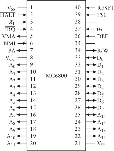
The VSS indicates Ground, and VCC is 5 volts. Like the 8080, the 6800 has 16 output Address signals and 8 Data signals used for both input and output. There's a RESET signal and a R/![]() (read/write) signal. The
(read/write) signal. The ![]() signal stands for interrupt request. The signal timing of the 6800 is considered to be much simpler than that of the 8080. What the 6800 doesn't have is the concept of I/O ports. All input and output devices must be part of the 6800 memory address space.
signal stands for interrupt request. The signal timing of the 6800 is considered to be much simpler than that of the 8080. What the 6800 doesn't have is the concept of I/O ports. All input and output devices must be part of the 6800 memory address space.
The 6800 has a 16-bit Program Counter, a 16-bit Stack Pointer, an 8-bit Status Register (for flags), and two 8-bit accumulators called A and B. These are both considered accumulators (rather than B being considered just a register) because there is nothing that you can do with A that you can't also do with B. There are no additional 8-bit registers, however.
The 6800 instead has a 16-bit index register that can be used to hold a 16-bit address, much like the register pair HL is used in the 8080. For many instructions, an address can be formed from the sum of the index register and the byte that follows the opcode.
While the 6800 does just about the same operations as the 8080—loading, storing, adding, subtracting, shifting, jumping, calling—it should be obvious that the opcodes and the mnemonics are completely different. Here, for example, are the 6800 Branch instructions:
Opcode | Instruction | Meaning |
|---|---|---|
20h |
| Branch |
22h |
| Branch If Higher |
23h |
| Branch If Lower or Same |
24h |
| Branch If Carry Clear |
25h |
| Branch If Carry Set |
26h |
| Branch If Not Equal |
27h |
| Branch If Equal |
28h |
| Branch If Overflow Clear |
29h |
| Branch If Overflow Set |
2Ah |
| Branch If Plus |
2Bh |
| Branch If Minus |
2Ch |
| Branch If Greater than or Equal to Zero |
2Dh |
| Branch If Less than Zero |
2Eh |
| Branch If Greater than Zero |
2Fh |
| Branch If Less than or Equal to Zero |
The 6800 doesn't have a Parity flag like the 8080, but it does have a flag the 8080 doesn't have—an Overflow flag. Some of these Branch instructions depend on combinations of flags.
Of course the 8080 and 6800 instructions sets are different. The two chips were designed about the same time by two different groups of engineers at two different companies. What this incompatibility means is that neither chip can execute the other chip's machine codes. Nor can an assembly-language program written for one chip be translated into opcodes that run on the other chip. Writing computer programs that run on more than one processor is the subject of Chapter 24.
Here's another interesting difference between the 8080 and the 6800: In both microprocessors, the instruction LDA loads the accumulator from a specified memory address. In the 8080, for example, the following sequence of bytes:
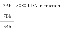
will load the accumulator with the byte stored at memory address 347Bh. Now compare that with the 6800 LDA instruction using the so-called 6800 extended addressing mode:
This sequence of bytes loads accumulator A with the byte stored at memory address 7B34h.
The difference is subtle. You expect the opcode to be different, of course: 3Ah for the 8080 and B6h for the 6800. But the two microprocessors treat the address that follows the opcode differently. The 8080 assumes that the low-order byte comes first, followed by the high-order byte. The 6800 assumes that the high-order byte comes first!
This fundamental difference in how Intel and Motorola microprocessors store multibyte values has never been resolved. To this very day, Intel microprocessors continue to store multibyte values with the least-significant byte first (that is, at the lowest memory address), and Motorola microprocessors store multibyte values with the most-significant byte first.
These two methods are known as little-endian (the Intel way) and big-endian (the Motorola way). It might be fun to argue over which method is better, but before you do so, be aware that the term Big-Endian comes from Jonathan Swift's Gulliver's Travels and refers to the war between Lilliput and Blefuscu over which end of an egg to break before eating it. Such an argument is probably purposeless. (On the other hand, I feel obliged to confess that the approach I used in the Chapter 17 computer wasn't the one I personally prefer!) Despite neither method being intrinsically "right," the difference does create an additional incompatibility problem when sharing information between systems based on little-endian and big-endian machines.
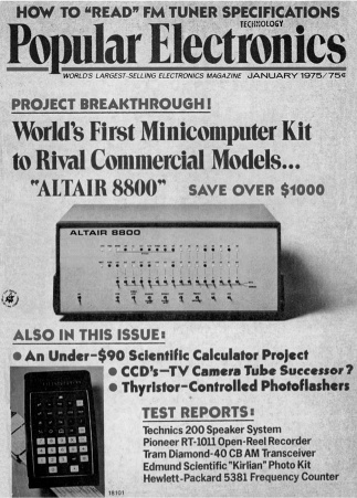
What became of these two microprocessors? The 8080 was used in what some people have called the first personal computer but which is probably more accurately the first home computer. This is the Altair 8800, which appeared on the cover of the January 1975 issue of Popular Electronics.
When you look at the Altair 8800, the lights and switches on the front panel should seem familiar. This is the same type of primitive "control panel" interface that I proposed for the 64-KB RAM array in Chapter 16.
The 8080 was followed by the Intel 8085 and, more significantly, by the Z-80 chip made by Zilog, a rival of Intel founded by former Intel employee Federico Faggin, who had done important work on the 4004. The Z-80 was entirely compatible with the 8080 but added many more very useful instructions. In 1977, the Z-80 was used in the Radio Shack TRS-80 Model 1.
Also in 1977, the Apple Computer Company, founded by Steven Jobs and Stephen Wozniak, introduced the Apple II. The Apple II, however, used neither the 8080 nor the 6800 but instead used MOS Technology's less expensive 6502 chip, which was an enhancement of the 6800.
In June 1978, Intel introduced the 8086, which was a 16-bit microprocessor that could access 1 megabyte of memory. The 8086 opcodes weren't compatible with the 8080, but I should note that they included instructions to multiply and divide. A year later, Intel introduced the 8088, which internally was identical to the 8086 but externally accessed memory in bytes, thus allowing the microprocessor to use the more-prevalent 8-bit support chips designed for the 8080. IBM used the 8088 chip in its 5150 Personal Computer—commonly called the IBM PC—introduced in the fall of 1981.
IBM's entrance into the personal computer market had a great impact, with many companies releasing machines that were compatible with the PC. (What it means to be compatible will be explored more in subsequent chapters.) Over the years "IBM PC compatible" has also implied "Intel inside," specifically Intel microprocessors of the so-called x86 family. The x86 family continued in 1982 with the 186 and 286 chips, in 1985 with the 32-bit 386 chip, in 1989 with the 486, and beginning in 1993, with the Intel Pentium line of microprocessors that are currently used in PC compatibles. While these Intel microprocessors have ever-increasing instruction sets, they continue to support the opcodes of all earlier processors starting with the 8086.
The Apple Macintosh, first introduced in 1984, used the Motorola 68000, a 16-bit microprocessor that's a direct descendant of the 6800. The 68000 and its descendants (often called the 68K series) are some of the most beloved microprocessors ever made.
Since 1994, Macintosh computers have used the PowerPC microprocessor that was developed in a coalition of Motorola, IBM, and Apple. The PowerPC was designed with a type of microprocessor architecture known as RISC (Reduced Instruction Set Computing), which attempts to increase the speed of the processor by simplifying it in some respects. In a RISC computer, generally each instruction is the same length (32 bits on the PowerPC), memory accesses are restricted to just load and store instructions, and instructions do simple operations rather than complex ones. RISC processors usually have plenty of registers to avoid frequent accesses of memory.
The PowerPC can't execute 68K code because it has a whole different instruction set. But the PowerPC microprocessors currently used in the Apple Macintoshes can emulate the 68K. An emulator program running on the PowerPC examines each opcode of a 68K program, one by one, and performs an appropriate action. It's not as fast as native PowerPC code, but it works.
According to Moore's Law, the number of transistors in microprocessors should double every 18 months. What are those many additional transistors used for?
Some of the transistors accommodate the increase in processor data width, from 4 bits to 8 bits to 16 bits to 32 bits. Another part of the increase is due to new instructions. Most microprocessors these days have instructions to do floating-point arithmetic (as I'll explain in Chapter 23); new instructions have also been added to microprocessors to do some of the repetitive calculations required to display pictures or movies on computer screens.
Modern processors use several techniques to help improve their speed. One is pipelining. When the processor is executing one instruction, it's reading in the next instructions, even to a certain extent anticipating how Jump instructions will alter the execution flow. Modern processors also include a cache (pronounced cash). This is an array of very fast RAM inside the processor that is used to store recently executed instructions. Because computer programs often execute small loops of instructions, the cache prevents these instructions from being repetitively reloaded. All these speed-improving features require more logic and more transistors in the microprocessor.
As I mentioned earlier, the microprocessor is only one part (although the most important part) of a complete computer system. We'll build such a system in Chapter 21, but first we must learn how to encode something else in memory besides opcodes and numbers. We must go back to first grade and learn again how to read and write text.