
The Fax Function
The public service telephone network (PSTN) has a frequency bandwidth of only about 3 kHz. Therefore, to transmit fax signals over it, considerable modification of the analog signals generated by an image scanner is required.
Standards for such transmission and reception have been established by an international body, the Consultative Committee for International Telephone and Telegraph (CCITT). Their recommendations have evolved over the years in groups. Today most fax operations conform to Group 3 standards. Their details are given later in this chapter.
CCD or CIS scanners derive analog signals from the documents which they scan. These have to be converted to digital form before being subjected to compression. Some time ago D.A. Huffman advanced a scheme for encoding signals so that less bandwidth is required for their transmission and reception. Since then other encoding schemes for compression have been advanced. One in particular is known as Modified Read (MR), a term derived from “RElative Address” coding. This encoding scheme reduces redundancy in the vertical direction as well as the horizontal direction. For that reason it is called “two dimensional.”
The raw data (namely, Non-Coded Format or NC data), which is read by a scanner, in a conventional facsimile, is converted or encoded “en bloc” into Modified Huffman (MH) data or Modified Read (MR) data. Further, in case of expanding MH data or MR data received by a conventional facsimile, NC data is decoded “en bloc” from the MH or MR data. Such an encoding or decoding operation is performed by using a large-scale integrated circuit (LSI) dedicated to encoding or decoding. Alternatively, such an encoding or decoding is effected by a general-purpose arithmetic and logic unit by using a central processing unit (CPU) of the conventional facsimile.
Further, image information corresponding to each line of a draft, which is read by the scanner of the conventional facsimile, is written to a memory as a bit string, of which each bit corresponds to a pixel. In case of performing a conversion of resolution of such image information (for example, condensing a draft image of size B4 into a converted image of size A4), a thinning of bits of a bit string corresponding to each line is performed at predetermined thinning intervals (for instance, every sixth bit, every seventh bit, every seventh bit, and every sixth bit corresponding to first, second, third, and fourth lines, respectively).
Another encoding scheme, borrowed from G4 fax, called “Modified Modified READ” (MMR), is also used in G3 fax machines. With it the image can be recorded as one long block of data, reducing the number of bits to be sent. This is possible because G4 protocols include error correction, making it unnecessary to provide a mechanism to define the end of the facsimile coded line to enable lines with errors to be detected.
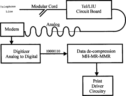
As shown in Figure 8.1, after compression the signal moves to a modem, where it is modulated into a form suitable for transmission over the narrow-band telephone line.

More details of modem operation are given later in this chapter. From the modem the signal passes to a telephone line interface circuit, which includes transformers for line isolation and surge protection circuits to prevent damage from line variations.
In the reception of fax messages, the procedure is reversed (Figure 8.2). Incoming analog signals pass through the telephone line interface circuit board to the modem. Then the modem turns them back to digital form so they go back as raw data to be decompressed to enable a printer to reproduce them in documentary form. Otherwise they may be fed to a PC, where they can be stored in its files or shown on its screen.
FAX CIRCUITRY
In MFPs, fax circuits are usually arranged on printed circuit boards in one of two ways. In some machines there is a digital board and an analog board. The digital board contains all of the signal processing and control functions followed by the modem. The output of the modem is fed to the analog board, which contains the circuitry necessary to interface with the telephone line. This circuitry includes the network interface, called the network control unit (NCU). See Figure 8.3.

Figure 8.3 General block diagram of digital and analog printed circuit boards (Kyushu Matsushita Electric Co., Ltd.).
(The following technical information on the digital and analog board is copyrighted by Kyushu Matsushita Electric Co., Ltd. and is reproduced here by permission of the Panasonic Services Company, a unit of the Matsushita Electric Corporation of America.)
In other machines there is a main board and line interface board. The latter contains the line interface unit (LIU). In this arrangement, all of the signal processing and control functions are included in a single integrated circuit called a fax engine. It feeds signals to and receives them from the modem on the same board. As mentioned above, the telephone interface circuitry is on a separate board and is called either an LIU or an NCU.
On the following pages both arrangements are described in detail.
CIRCUIT OPERATIONS
The control section will be explained as shown in the block diagram (Figure 8.4).

1. CPU (IC401): The CPU fetches and executes instructions from ROM, writes (reads) data to (from) RAM, writes commands to the ASIC, and reads status information from ASIC.
2. ROM (IC402): Contains all of the program instructions for unit operations.
3. Static RAM (IC403): This memory is used mainly for parameter working storage area.
4. Dynamic RAM (IC407): This memory is used mainly for parameter working storage area.
5. RTC (IC409): Real time clock.
6. ASIC (IC404): Composed mainly of address decoder and modem control section. Controls the general FAX operation. Controls the operation panel I/F. Controls the thermal head I/F and CCD I/F. Execution image processing.
7. ASIC 2 (IC412): Resolution degree conversion, central I/F.
8. MODEM (IC405): Executes modulation and demodulation for FAX communications.
9. Read Section: CIS image sensor to read transmitting documents.
10. Motor Driver (IC406): Drives the transmission motor and the reception motor.
11. Reset Circuit (IC410): Provides reset pulse to each of the major ICs.
Operation Board
1. G/A (IC301): Digital board and serial communication.
2. Sensor: Document set sensor (PI302); read position sensor (PI301); cover open sensor (PI303).
CPU (IC401)
The KX-F1600 uses a TMP96CO31 CPU operating at 16 MHz.
Pin Chip Carrier Pin Assignments Pin descriptions (see Figure 8.5):

AD0–AD15: Address/Date Bus (input/output).
A16–A23: Address Bus (output).
RD: Read (output, active Low). RD indicates that the CPU wants to read data from AD0–AD15.
WR: Write (output, active Low). WR indicates that the CPU Address/Date bus (AD0–AD7) holds valid data.
HWR: Write (output, active Low). HWR indicates that the CPU Address/Date bus (AD8–AD15) holds valid data.
ALE: Address Latch Enable (output, active High). ALE indicates that the CPU Address/Date bus (AD0–AD15) holds valid address.
RESET: Reset (input, active Low).
RAS: Row Address Strove (output, active Low). DRAM interface.
CAS: Column Address Strove (output, active Low). DRAM interface.
ROM (IC402)
The 256 Kb ROM (EPROM or MASKRQM) is used to store programs. The address is 000000H–O3FFFFH.
Static RAM (1C403)
The 32 Kb SRAM that is backed up with a lithium battery is used. This holds one-touch dial, automatic dial, and ID, etc. The address is 30000011–307FFFH.
Dynamic RAM (IC407)
DRAM is used for CPU work. The address is 4400000H-47FFFFH. Refresh is executed every 16.2 μs. See Figure 8.6.

ASIC (IC404)
This custom IC is used for general fax operation (Figure 8.7).

1. Decoder: Decodes the address of the CPU (IC401) according to the memory map.
2. CPU I/F: Outputs the INTERRUPT signal.
3. ROM/RAM I/F: Controls the SELECT signal of ROM or RAM.
4. CIS I/F: Controls document reading.
5. IMAGE DATA RAM. Inside ASIC and 8 KB. Figure 8.8 indicates the mapping which is used in image processing.

6. TX MOTOR I/F: Controls the transmission motor which feeds the document.
This memory is built in to the ASIC (IC404) to be used for image processing. The memory map of image data RAM is shown in Figure 8.8.
ASIC 2 (IC412)
This ASIC function (Figure 8.9) performs the following:
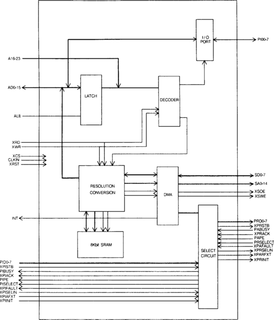
1. The fax receiving or copy time’s 200-dpi data is converted to the printer resolution degree, 360 dpi. Also, by changing the conversion rate, the image can be reduced.
2. The host’s (personal computer’s) central data (from CN412) and the fax data can be exchanged.
Also, when performing the main scanning direction conversion in the hardware, work RAM (IC418) is necessary.
Reset Circuit
The output from pin 3 of the Reset IC (IC410) resets the CPU (IC401), ASIC 1 (IC404), ASIC
2 (IC412), the modem (IC405), the gate array on the operating board (IC301), the Port IC (IC 1) on the analog board through the IC414.
1. During a momentary power interruption, a positive reset pulse of 175 ms or more is generated and the system is reset completely (Figure 8.10). This is done to prevent partial resetting and system runaway during power fluctuation.

2. When pin 3 of the IC410 becomes low-level, it will prohibit the RAM (IC403) from changing data (Figure 8.11). The RAM (IC403) go into the backup mode, when they are backed up by the lithium battery.
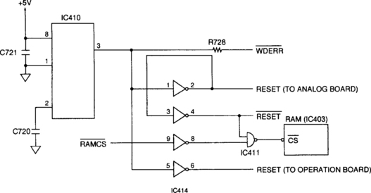
3. The watchdog timer, built into the gate array (IC404), is initialized by the CPU (IC401) about every 1.5 ms (Figure 8.12). When the watchdog error occurs, pin 114 of the gate array (IC404) becomes low level. The terminal of the WDERR signal is connected to the reset line, so the WDERR signal works as the reset signal.

SRAM Backup Circuit
1. Function. This unit has a lithium battery (BATT), which works for the RAM (IC403) and Real Time Clock IC (RTC, IC409). The user parameters of autodial numbers, the transmission ID, the system setup date, and so on are stored in the RAM (IC403). The RTC (IC409) continues functioning even when the power switch is OFF, when backed up by the lithium battery.
2. Circuit operation. See Figure 8.13. When the power switch is turned ON, thus supplying the power through the IC410 to the RAM (IC403) and RTC (IC409), at this time, the voltages at pin 28 of the RAM and pin 8 of the RTC are +5 V. When the power switch is turned OFF, the BATT supplies the power to the RAM and RTC through the JMP1, R701, and IC409. At this time, the voltages at pin 28 of the RAM and pin 8 of the RTC are about +2.5 V When the power switch is OFF and the voltage of +15 V goes down, the Reset IC (IC410) outputs the reset signals. Pin 28 of the RAM (IC403) and pin 8 of the RTC (IC409) become low level, and then the RAM and RTC go into the back-up mode, when the power consumption is less.

IMAGE DATA FLOW DURING FACSIMILE OPERATION
Copy (Fine, Super-Fine, Half Tone)
See Figure 8.14.

Figure 8.14 Block diagram of image flow during fax operation (Kyushu Matsushita Electronic Co., Ltd.).
1. Line information is read by CIS, by way of route, and it is inputted to IC404.
2. In IC404, data is adjusted to a suitable level for A/D conversion at the Analog Signal Processing Section, and by way of route (2), it is inputted to A/D conversion (8 bit). After finishing A/D conversion, data is inputted to the Image Processing Section by way of route (3), and by way of routes (4) and (5), it is stored in RAM as shading data.
3. Draft information that is read by CIS is inputted to IC404 by way of route (1), and after adjusting to suitable level for A/D conversion by way of route (2), draft information is converted to A/D (8 bit) and is inputted to the Image Processing Section. The other side, the shading data that flows from RAM by way of routes (6) and (7), is inputted to the Image Processing Section. After the draft information’s image processing is finished, white is regarded as “0” and black is regarded as “1”; by way of routes (4) and (5), they are stored in RAM.
4. The white/black data stored in step 3 passes through routes (6), (8), and (9). Then it is stored in RAM (IC407). (Note: Standard Read 3.58 times/mm; Fine Read 3.58 times/mm; Read 7.7 times/mm.)
5. The data stored in RAM (IC407) passes through route (11) and is input into ASIC 2 (IC412). The input data then works through RAM (IC418) by routes (12) and (13), while exchanging the 200-dpi data to 360-dpi data.
6. The data changed to 360 dpi passes through route (14) and is output to the printer. Then it is printed.
Transmission
1. Processing proceeds as for copying, items 1–3.
2. Data stored in RAM of 1C404 is outputted from IC404 by way of routes (6) and (8) and is stored in the system bus. By way of route (9), it is stored in the communication buffer inside DRAM (IC407).
3. While fetching data stored in the communication buffer synchronous with the modem, CPU (IC401) inputs data to the modem along route (10), where it is converted to serial analog data and forwarded over telephone lines via the NCU section.
Reception
1. Serial analog image data is received over telephone lines and input to the modem via the NCU section, where it is demodulated to parallel digital data. Then the CPU (IC401) stores the data in the communication buffer DRAM (IC407) along route (10).
2. Data stored in DRAM (IC407) is decoded by CPU (IC401) by way of route (10) and is stored in DRAM.
THE FAX ENGINE
To go with its FAX modems Rockwell has developed MPUs called fax engines. Combined with a modem as shown in Figure 8.15, they may look like a great simplification over the digital-analog board arrangement. However, several other smaller chips are required on the main board to perform essentially the same functions as those carried out on the digital board. Despite this, the combination of the Rockwell fax engine and modem is used by quite a few manufacturers to provide what is literally the heart of the fax circuitry in PC multifunctional peripherals. To show the fax engine chip with its 160 pins would serve no useful purpose, because Rockwell treats the internal functions of the chip as proprietary information.

THE FAX MODEM
As mentioned earlier in this chapter, the CCITT has established standards for modulation schemes so modems can communicate with each other. They are designated by V. and, insofar as fax is concerned, have progressed from V.21 to V.34. V.21 is a data transmission standard at 300 bits per second (bps). Its modulation is frequency shift keying (FSK) and is used for the calling signal. Above that level, the most important modulation standards for fax modems in MFPs for PCs are V.29 and V32. V.29 handles up to 9,600 bps and downward to 7,200 and 4,800 bps. V.32 handles up to 14,400 bps and downward to 4,800 bps. A third standard, V.34, handles up to 33,600 bps. However, the highest modem speed in MFPs for PCs is 14,400 bps at this time. All of the preceding standards allow the modem to fall back to bit rates below its maximum rate to communicate with older machines, which do not have the higher rate capability.
A standard below V.29, V.27ter uses phase shift keying (PSK) modulation. V.29 and higher levels use quadrature amplitude modulation (QAM).
A typical present-day modem architecture is shown in Figure 8.16. Such modems have a controller and a signal processor that are electrically connected to each other through an interface circuit. The controller provides supervisory functions in the modem, such as inserting control commands in the data stream for error and flow control, which is normally referred to as the “link layer,” and providing data compression. The signal processor, the codec, and the interface circuit together form a data pump that is responsible for carrying out the digital communication portion of the modem, including startup, retrains, modulation, demodulation, channel equalization, echo cancellation, and timing recovery. As a result, the data pump is responsible for implementing various CCITT standards of the modem—such as the V.34 standard, which establishes 28.8 Kb/s two-way communication. Basically, the controller supervises the data stream and the signal processor prepares the stream for communication over a predetermined medium (i.e., a telephone line).

As shown in Figure 8.16, the controller and the signal processor of a typical modem have separate memory resources, and thus separate memory and I/O registers and buses. The memory dedicated to the controller is composed of memory for instructions (e.g., ROM), and memory for data, including scratchpad or RAM, wherein the RAM can be used to provide a controller stack, a dictionary for the compression engine, and a space where data is prepared for transmitting and/or evaluated when received.
The memory dedicated to the signal processor is composed of memory for instructions (i.e., ROM) and scratchpad memory for signal processing functions such as storing the intermediate values of the received modem waveform. In addition, for modulation needs, the signal processor needs to store slow “symbol” data that is saved in the signal processor RAM as bulk delay information, wherein the bulk delay is used for long distance calls encountering satellite hops (less than two). In today’s modems, the bulk delay usually takes up to 50% of the signal processor RAM.
Rockwell International has chosen to implement their modems as dedicated circuits rather than as general-purpose DSP circuits, so they can optimize performance and reduce chip size. In the Rockwell family of modems, the dedicated data pump is driven by a single chip controller that can be supplied by them or several other vendors. An outboard compression/expansion processor may be added to the configuration for higher performance. This dedicated hardware offers the advantages of low cost, low parts count, and less external memory to support the modem.
NCU PCB
The NCU PCB switches the communications line to telephone or built-in modem, under control of the main PCB. Also, it works as a power supply interface from the power supply unit to the main PCB and the recording head. (See Figure 8.17.)

Figure 8.17 Block diagram of NCU printed circuit board. (permission granted by Brother International)
(The following general description of the NCU is presented with permission granted by Brother International.) The NCU PCB consists of the following components: noise filter, line relay, line transformer, circuit related to line transformer, high impedance transformer circuit, calling signal detector, loop current detector, dial pulse generator, telephone circuit, and recording head interface.
• The primary function of the NCU that is shared by facsimile and telephone units is to switch a line to the facsimile unit or to the telephone. This switching is carried out by the line relay.
• Since the direct connection of facsimile equipment to the line is not allowed in order to protect the line, it is essential to insert a line transformer between the line and the facsimile equipment to insulate them from each other.
The preceding two components, a line relay and a line transformer, are the minimum requirements for the NCU of the facsimile equipment.
• If an external telephone is attached to the facsimile equipment, the NCU should have a loop current detector to identify the hook state by detecting loop current.
• If the facsimile equipment has an automatic answering facility, the NCU should be equipped with a calling signal detector that detects a calling signal and tells it to the CPU in the fax engine.
• The circuit related to a line transformer allows the line transformer to be invariant by selecting the constants of the parts in this circuit so as to conform to the communications regulations or codes of each country.
In addition to the preceding basic components of the NCU, the following components are also required, depending on the additional functions of the facsimile equipment:
• The dial pulse generator generates dial pulses within the facsimile equipment.
• The surge absorber is a protection circuit that absorbs lightning surge.
• The noise filter eliminates noise, including radiation noise, to prevent it from flowing out onto the communications line.
• The high-impedance transformer circuit detects remote activation and F/T switching sent from the line in the ON-HOOK state without any interference to the line.
• The telephone circuit includes two amplifiers: one for amplifying the output signals of the handset microphone, and the other for amplifying the receive signals from the communications lines to sound the handset receiver.
G3 FAX BINARY PROTOCOL
Figure 8.18 diagrams a normal sequence of automatic calling and called operations by the G3 facsimile binary protocol. The left side shows the calling station and the right side shows the called station. The calling station calls the called station by a dial signal. When the called station is connected, the calling station sends a calling tone (CNG). The called station responds to this by sending a tonal signal for called equipment identification (CED).

Then, the called station sends a digital identification signal (DIS) in binary form representing a communication condition. Until the calling station sends a digital command signal (DCS) in response to the DIS signal, the called station repeatedly resends the DIS signal for 30–40 s.
The calling station sends the DCS signal in accordance with the content of the DIS signal, sets a communication rate and a specification, sends a training signal and checks data, and checks whether or not the called station can correctly receive data.
If the called station correctly receives data, it sends back confirmation of ready to receive (CFR) in binary form. If it cannot receive data, it sends back failure to train (FTT) in binary form and restarts from the DCS signal with a reduced transmission rate as required. If the calling station does not send an image signal within 6 s after it has received CFR, it is interpreted as an error and the line is disconnected. Thus, the communication function unit must have received the image data from the host by that time. According to the CCITT Recommendation T.4, the G3 facsimile machine uses an MH or MR (modified read) compression method to compress the image signal. Normally, the MH compression is carried out and an end of line (EOL) code is added to each line. A minimum transmission time of one line of image is determined by DIS and DCS to be one of 0, 5, 10, 20, and 40 ms. Similarly, a maximum transmission time of one line is defined as 5 s. Accordingly, when the data transmission rate of the host is low, a fill (continuous “0”s) is inserted between the data and the EOL. However, since it is rare that the data is delayed, an error takes place in a commercially available facsimile machine if a long fill is inserted such that previous data is inserted by a line error or drive of a paper feed motor is stopped and the image is rendered discontinuous. Accordingly, it is not possible to reduce the transmission rate by inserting too much fill.
At the end of the image data, Q represents end of message (EOM), multipage signal (MPS), and end of protocol (EOP), in binary form. For EOP, the called station sends message confirmation (MCF) and the calling station sends the disconnect command (DCN) to disconnect the line.
If further image data is to be sent under the same conditions, MPS is sent and the next page of data is sent within 6 s after the reception of MCF. EOM is used when further image data is to be sent under another condition. In this case, the process returns to the initial DIS signal.
FILE TRANSFER
In the above protocol, there are essentially five phases:
Phase A is the call establishment and line connection of equipment
Phase B is the premessage signaling and capability selection
Phase C is the facsimile message transfer
In particular, phase B is the low-speed (300 baud) premessage signaling in which the capabilities of the respective machines are indicated and selected. In particular the called station first responds with a Digital Information Signal (DIS) in which its capabilities in terms of group type, speed, resolution, and other special capabilities are indicated. At this time file transfer capabilities may also be indicated. The calling machine then responds with a Digital Command Signal (DCS) in which, in line with its own capabilities, the capabilities required for the forthcoming transmission are selected. This is followed by a high-speed training sequence related to synchronization, equalization, and other functions.
When the receiving machine indicates its readiness to receive, phase C is entered, during which the transfer of facsimile information takes place. At this time the transmitting machine will progressively scan the input document, code and compress the pixel information according to the selected resolution, and transmit the information at the selected speed. The receiving machine will correspondingly decompress and decode the received information and print the required image.
At the completion of each page, phase D is entered. This post-message signaling determines if there are more pages to transmit, in which case phase C is repeated. If there are no more pages, then phase E is entered.
It is necessary to refer to recent modifications to the standards for facsimile telecommunications as determined by Study Group VIII of the CCITT. These allow for improvements in speed, resolution, and network addressing procedures, and also for file transfer to be accomplished as an alternative facsimile data type.
The procedures for nonfacsimile image data transfer within the facsimile call are defined in modifications and appendices to the CCITT Recommendations T.4 and T.30, which govern facsimile telecommunications. In particular, the file transfer modes permitted are as follows:
Of these, BFT is considered most general and most suitable for widespread application for PC-compatible communications. This is because the binary file mode allows the transfer of any type of file, including those indicated by the other modes. The first two transfer modes are more appropriate for integration with telex or similar communications, whereas the fourth relates specifically to the standard form for electronic data interchange for administration commerce and transport (EDIFACT).
While the binary file transfer mode will be most relevant, it may be preferred to include equipment capable of transceiving file information in any of the listed modes and interfacing with equipment that is designed specifically for the transception of information in any of the listed file transfer modes.
File transfers may be effected, with a compatible receiver, by making the appropriate DCS selection in phase B. This may be after the completion of a normal facsimile transfer in phase C. In this case, Error Correction Mode (ECM) will also be selected to guarantee data integrity. File transfer will take place in phase C according to the BFT or other selected file transfer mode.
In the case of a facsimile device for a personal computer, the file or files selected for transfer, and those received, will normally reside on the hard disk or floppy disk of the personal computer, according to the user’s specification. In the case of non-computer-based devices, the files for transception will normally reside on a floppy disk.
With all facsimile devices the facility may exist for the calling device to receive facsimile information from a remote called device that has a document to transmit (polling). This facility is also relevant for file transfers, as per CCITT Recommendation T.30.
PC FAX
A function to directly fax image data from a personal computer and to receive image data faxed to a personal computer is called PC fax. Prior to the development of multifunction peripherals, this operation was implemented primarily by connecting fax boards or cards between the PC and the telephone line. With such units it is possible to receive faxes, print them, and store them on the hard disk in the PC. It is also possible to create outgoing faxes for text and graphics files as well as images that have been scanned in the PC files.
With the advent of MFPs for PCs, it has been possible to perform all operations with board and card attachments and to eliminate most of their shortcomings. These include being able to receive faxes with the PC turned off, and being able to do multitasking (receive faxes while printing or copying). Also, software packages and special types of software can be used to support PC faxing via the MFP.
An example of software application to the fax function is provided by Samsung in their models Msys 4700 and Msys 4800. When installed in the PC, their SmartSoft CD-ROM provides a fax driver, which is a Windows program that runs silently in the background all of the time. By installing a program called SmartFAX in the PC, it is possible to control fax operation in Windows 95 or Windows 3.x.
SMARTFAX
When SmartFAX is started, the image shown in Figure 8.19 is displayed. The figure also indicates the various options that can be selected from the PC keyboard and/or mouse.

Sending a Fax
Start SmartFAX and select options as required.
Resolution
Change the resolution to increase sharpness and clarity. FINE is good for documents containing small characters or thin lines, or print from a dot-matrix printer. SUPER FINE works well for documents containing extremely fine detail. SUPER FINE works only if you start sending using the SEND/START button and if the remote machine also has the SUPER FINE feature.
Contrast
Change the contrast if the faxed document should be lighter or darker than the original document.
Document Type
Select the document type from TEXT or PHOTO.
Enter the fax number using the computer keyboard or the number keypad on the SmartFAX window, or click the desired phonebook number if a fax number has been stored into the phonebook memory. The number will appear in the display.
If more than one page is to be sent, click MEM TX. The machine does not send the document as it scans it. The document will be scanned into memory and the machine will immediately eject the original, freeing the document tray.
Sending begins after all the documents are scanned into memory.
If a document is to be sent directly from the tray without scanning it into memory, SEND/START is used. Sending begins immediately.
Receiving a Fax
Receiving Automatically in Fax Mode
1. FAX must be selected in the SmartFAX window.
2. The machine answers the call after the number of rings specified in the Ring Before Answer option.
If memory gets full while receiving a fax, the reception is automatically canceled.
Some receiving features can be changed, for example, ring count, automatic reduction, and discard, setting through the SmartFAX program on the PC.
The cartridge can be replaced while receiving a fax. The receiving data will be temporarily stored into the machine’s memory and printed after you replace the cartridge.
Receiving Manually in TEL Mode
Set your Msys 4700 or Msys 4800 machine to receive a fax manually when each incoming call is checked to see if it is from a fax or from a person.
1. Make sure that TEL is selected in the SmartFAX window.
2. When the machine rings, the handset is picked up and the call is answered.
3. If a fax tone is heard, or if the person on the other end asks that a fax be received, press the Start/Enter button on the Msys 4700 or Msys 4800 machine, then hang up the phone.
Receiving Automatically in TEL/FAX Mode
1. Make sure that TEL/FAX is selected in the SmartFAX window.
2. When a call comes in, the machine answers the call on the second ring, and receives a fax signal automatically. The number of rings can be changed.
3. If the machine does not sense a fax signal, it will give another ringing tone to indicate that it is a phone call.
4. Lift the handset to answer the call. If the handset is not picked up within a specified time, the machine will switch to automatic fax reception mode.
Using Phonebook
SmartFAX makes it possible to set up a personal phonebook in the personal computer and download it to Msys 4700 or Msys 4800 multifunction machines. Frequently used fax numbers (up to 70) may be stored into the phonebook memory. The numbers are easily accessed by clicking the BOOK button on the SmartFAX.
Storing Numbers into and Deleting Numbers from Phonebook
1. Start the SmartFAX if not already started. The SmartFAX window will appear.
2. Click BOOK on the SmartFAX window. The Phonebook dialog box will appear.
3. Select the desired phonebook number in the phonebook list and click the Edit button. The Edit dialog box will appear.
Note: If the Delete button on the Phonebook dialog box is clicked, all information stored into the selected phonebook number will be deleted.
4. Enter any name and number and click OK to save the information just entered. The name includes all capital letters, numbers, spaces, and special symbols („ ., /, +, *, &, –, #).
The phonebook keys in which fax numbers are stored appear in blue on the SmartFAX window.
Sending Phonebook Numbers from SmartFAX to Msys 4700 or Msys 4800 Machines
After numbers are stored in the SmartFAX phonebook, they can be sent to your Msys 4700 or Msys 4800 machine by pressing the Send Phone Book button in the Phonebook dialog box. All the numbers in the SmartFAX phonebook will be downloaded to the machine. The phonebook numbers 1 through 20 will substitute for one-touch dial numbers, and the phonebook numbers 21 through 70 will substitute for speed dial locations 01 through 50.
Getting Phonebook Numbers from Msys 4700 or Msys 4800 Machine to SmartFAX
The numbers currently stored in your Msys 4700 or Msys 4800 machine can be retrieved by pressing the Get Phone Book button in the SmartFAX phonebook dialog box. The numbers will be uploaded to the SmartFAX. The one-touch dial numbers 1 through 20 will substitute for the SmartFAX phonebook numbers 1 through 20, and the speed dial numbers 01 through 50 will substitute for SmartFAX phonebook numbers 21 through 70.
Setting User Options
The SmartFAX allows for specifying user-selectable features for faxing and copying.
Selectable Options
• Terminal ID: The terminal ID—a number and name—will be printed at the top of each page faxed from the machine.
• Receive Mode: Manual or Automatic receiving mode may be selected. For automatic receiving, select FAX, TEL/FAX, ANS/FAX. For manual receiving, select TEL.
• Paper Size: A4, Letter or Legal paper size may be selected to be used for printing a received fax or a copy.
• Print Quality: Select LQ to print a fax in low speed with high quality. If Draft is selected, the machine prints in high speed with low quality. To maintain the best possible print quality in Draft mode, the cartridge needs to be aligned from the control Program on the printer driver.
• Discard Size: When receiving or copying a document as long as or longer than the paper installed in the machine, the machine may be set to discard any excess image at the bottom of the page to fit into the recording paper size.
If the received page is outside the margin set, it will be printed on two sheets of paper at the actual size.
If the Auto Reduction feature is turned on, it will be reduced to fit into the appropriate size paper (Discard does not take place). If the Auto Reduction feature is turned off or fails, the data within the margin will be discarded.
Enter the desired discard size (from 0 to 30 mm).
• ECM: This mode compensates for poor line quality and ensures accurate, error-free transmission with any other ECM-equipped facsimile machine. If the line quality is poor, transmission time may be increased when ECM is enabled. ECM mode will be activated when a fax is sent using the MEM TX button. To turn this feature on, select On. To turn this feature off, select Off.
• Remote RCV MF Code: The remote receive MF code allows the initiation of fax receive from an extension phone plugged into the EXT jack on the back of the machine. If the extension phone is picked up and a fax tone is heard, enter the remote receive code and the fax will start receiving. The password is preset to • 9 • at the factory. Enter the desired code 0 to 9 on the number keypad.
• Dial Mode: Select the type of dial mode, Tone or Pulse.
• Ring Before Answer: Select the number of times the machine should ring before answering an incoming call. Enter the desired ring number (from 1 to 7).
• Auto Reduction: When receiving a document as long as or longer than the paper installed in the machine, the machine can reduce the data in the document to fit into the recording paper size. This feature may be turned on to reduce an incoming page that may otherwise need to be divided into two pages with only a few centimeters on the second page. If the fax machine cannot reduce the data to fit into one page with the feature enabled, the data is divided and printed in actual size on two or more sheets if needed. Select On to turn this feature on. Select Off to turn this feature off; the overflow data will be printed out on a second page.
Setting Options
1. Start the SmartFAX, if not already started. The SmartFAX window will appear.
2. Click MENU on the SmartFAX window, and select Settings from the menu. The Settings dialog box will appear.
Note: When changing the settings on the SmartFAX, or when starting the SmartFAX, the user options setting on both the Msys 4700 or Msys 4800 machine and the SmartFAX program will be updated to the latest settings made either on the machine or on the SmartFAX.
Printing Out Lists
The SmartFAX allows you to check lists containing useful information and to print out if needed. The following lists are available:
• TX (Transmission) or RX (Reception) Journal: This report shows information concerning transmission or reception activities.
• Phone Number: This list shows all the numbers currently stored in the phonebook memory.
• Settings: This list shows the status of the user-selectable options.
To monitor and print the list, do as follows:
1. Start the SmartFAX, if not already started. The SmartFAX window will appear.
2. Click MENU on the SmartFAX window, and select List Out from the menu. The List Out dialog box will appear.
3. Select the desired list, and click OK.
4. The selected list dialog box will appear. If desired, click Print on the dialog box.