
4
Energy Measurement
Pulse processing systems designed to measure the energy spectrum of radiation particles are known as energy spectroscopy or pulse‐height spectroscopy systems. The spectroscopy systems have played an important role in a number of scientific, industrial, and medical situations since the early 1950s, and their performance has continuously evolved ever since. In recent years, the improvement in the performance of radiation spectroscopy systems has been centered on using digital and monolithic pulse processing techniques though classic analog systems are still widely used in many situations. In this chapter, we discuss the principles of analog pulse‐height measurement systems, but many of the concepts introduced in this chapter are also used in the design and analysis of the digital and monolithic pulse processing systems. We start our discussion with an introduction to the general aspects of energy spectroscopy systems followed by a detailed description of the different components of the systems.
4.1 Generals
In Chapter 1 we saw that the total induced charge on a detector’s electrodes is proportional to the energy lost by radiation in the sensitive region of the detector. This means that the amplitude of a charge pulse represents the energy deposited in the detector, and therefore, a spectrum of the amplitude of the charge pulses essentially represents the distribution of energy deposition in the detector and is produced by using a chain of electronic circuits and devices that receive the pulses from the detector, amplify and shape the pulses, and digitize the amplitude of signals to finally produce a pulse‐height spectrum. The basic elements of such system are shown in Figure 4.1. In most of the situations, a charge‐sensitive preamplifier constitutes the first stage of the pulse processing system though there are situations in which a current‐ or voltage‐sensitive preamplifier may be used. The preamplifier output is usually taken by an amplifier/shaper, sometimes simply called linear amplifier, which is a key element in the signal chain and has a twofold function: First it provides enough amplification to match the amplitude of the pulse to the input range of the rest of the system. Second, it modifies the shape of preamplifier output pulses in order to optimize the signal‐to‐noise ratio and to minimize the undesirable effects that may arise at high counting rates and also from variations in the shape of the input pulses. In terms of electronic noise, a linear amplifier can be considered as a band‐pass filter: it has a combination of a high‐pass filter to reduce the duration and low frequency noise and a low‐pass filter to limit the noise bandwidth. The high‐pass part is often referred to as a differentiator, while the low‐pass part is referred to as an integrator. The midband frequency of the band‐pass filter ωsh is chosen to maximize the signal‐to‐noise ratio. It is customary to characterize linear amplifiers in the time domain through the shaping time constant τ that is, in a first approximation, related to ωsh by τ ≈ 1/ωsh. In terms of count rate capability, a linear amplifier replaces the long decay time of the preamplifier output pulses with a much shorter decay time, thereby isolating the separate events. The output of a linear amplifier is processed with a dedicated instrument called multichannel pulse‐height analyzer (MCA), which produces a pulse‐height spectrum by measuring the amplitude of the pulses and keeping the track of the number of pulses of each amplitude. The pulse‐height spectrum is then a plot of the number of pulses against the amplitude of the pulses. An MCA essentially consists of an analog‐to‐digital converter (ADC), a histogramming memory, and a device to display the histogram recorded in the memory. The ADC does a critical job by converting the amplitude of the pulses to a digital number. The conversion is based on dividing the pulse amplitude range into a finite number of discrete intervals, or channels, which generally range from 512 to as many as 65 536 in larger systems. The number of pulses corresponding to each channel is kept by taking the output of the ADC to a memory location. At the end of the measurement, the memory will contain a list of numbers of pulses at each discrete pulse amplitude that is sorted into a histogram representing the pulse‐height spectrum. The term MCA was initially used for stand‐alone instruments that accept an amplifier’s pulses and produce the pulse‐height spectrum. With the advent of personal computers, the auxiliary memory and display functions were shifted to a supporting computer, and specialized hardware for the pulse‐height histogramming were developed. Such computer‐interfaced devices are called multichannel buffer (MCB). It is important to note that an MCA or MCB essentially produces a spectrum of the amplitude of input pulses, and thus it is also widely used in applications other than energy spectroscopy where the amplitude of the input pulses to MCA may carry information such as timing, position, and so on.

Figure 4.1 Simplified block diagram of an MCA‐based energy spectroscopy system and signals waveforms in different stages.
In some applications, it is only required to select those pulses from amplifiers whose amplitude falls within a selected voltage range, that is, an energy range. This task is performed by using a device called single‐channel analyzer (SCA), which has a lower‐level discriminator (LLD) and an upper‐level discriminator (ULD) and produces an output logic pulse whenever an input pulse falls between the discriminator levels, called the energy window. The outputs of a SCA can be then counted to determine the number of events lying on the energy window or used for other purposes. Before the invention of MCA, SCAs were also used to record the energy spectra by moving the SCA window stepwise over the pulse‐height range of interest and counting the number of pulses in each step. A better approach was to count the number of events in each energy window with a separate SCA connected to a separate counter. The energy spectrum is then produced by plotting the measured counts versus the lower‐level voltage of the windows. It is obvious that compared with what can be accomplished with an MCA, the use of SCA for energy spectroscopy is a very inconvenient process, but SCA is still a very useful device for applications that require the selection of the events in an energy range.
In all elements of radiation detection systems including detector and pulse processing circuits, there is a finite time required by each element to process an event during which the element is unable to properly process other incoming signal pulses. The minimum time separation required between the successive events is usually called dead time or resolving time of the detector or circuit. The minimum time required for the whole system to accept a new pulse and to handle it without distortion is called the dead time or resolving time of the system. Because of random nature of radioactive decay, there is always some probability that a true event is lost because it occurs during the dead time of the system. A low dead‐time system is of importance for high input range measurements and also in quantitative measurements where the true number of detected particles is required.
4.2 Amplitude Fluctuations
A pulse‐height spectroscopy system should ideally measure the same amplitude (or channel number) for pulses that resulted from the same amount of energy deposition in the detector. However, even with an ideal MCA with infinite number of channels and uniform conversion gain, this is never practically achieved because of the presence of several sources of fluctuations in the amplitude of the pulses that stem from the pulse formation mechanism in the detector and from the imperfections in the pulse processing system. Therefore, a real pulse‐height spectrum for a constant amount of energy deposition has a finite width as it is shown in Figure 4.2. The spread in the distribution of amplitudes of the pulses is generally modeled with a Gaussian function, though there are situations in which deviations from a Gaussian function are observed. The energy resolution is the full width at half maximum (FWHM) of the Gaussian function ΔHfwhm, and the relative energy resolution of a detection system at a given energy is conventionally defined as
where H˳ is the peak centroid that is proportional to the average amplitude of pulses or particle’s energy. Figure 4.3 shows the effect of energy resolution on the separation of events of close energy deposition. A spectrometry system with poor energy resolution has a large width and thus is unable to distinguish closely spaced spectral lines that are produced if two energies differ only by a small amount.

Figure 4.2 (a) An ideal distribution of the amplitude of the pulses for the same amount of energy deposition in a detector. (b) A realistic distribution of the amplitude of the pulses described with a Gaussian function.

Figure 4.3 The effect of energy resolution on the separation of two close energy lines.
4.2.1 Fluctuations Intrinsic to Pulse Formation Mechanisms
4.2.1.1 Ionization Detectors
In ionization detectors, not all the deposited energy is used for producing free charge carriers. In semiconductor detectors, a variable amount of energy may be lost in producing vibrations in the crystal lattice that cannot be recovered. In gaseous detectors, some of the energy is lost by the excitations of gas molecules that do not lead to ionization. Since these processes are of statistical nature, the number of free charge carriers varies from event to event and the resulting fluctuations are called Fano fluctuations [1]. The FWHM of the spread in the amplitude of the pulses due to Fano fluctuations is given, in unit of energy, by
where w is the average energy required to produce a pair of charge carriers, E is the energy deposition in the detector, and F is the Fano factor, which is always less than unity and is generally smaller in semiconductor detectors than gaseous mediums. The pair creation energy in gaseous detectors is approximately ten times larger than that in semiconductor detectors, and thus FWHMstat is more significant in gaseous detectors. The number of charge carriers in some detectors such as proportional counters and transmission charged particle detectors is subject to further fluctuations due to particles’ energy loss inside the detector and/or charge multiplication process.
The second source of fluctuations in the amplitude of the pulse stems from the process of charge collection inside the detectors. The drifting charges toward the electrodes may be lost due to trapping effects or recombination processes that prevent them from charge induction on the electrodes. In general, this contribution depends on the material and technology employed in the detector fabrication and is related to the intensity of electric field. One may quantify such fluctuations with the FWHM of the spread in the amplitude of the pulses (FWHMcol). The fluctuation in charge collection is most significant in semiconductor detectors of large size or poor charge transport properties but can be negligible in high quality detectors.
The third source of fluctuations in the amplitude of pulses is due to the electronic noise. It was discussed in previous chapters that the electronic noise is always present in the detector circuits and results primarily from detector and preamplifier, but it can be reduced with a proper pulse shaping that eliminates out‐of‐band noise. Figure 4.4 illustrates that when a noise voltage with root‐mean‐square value of erms is superimposed on pulses of constant height, the resultant pulse‐height distribution has a mean value equal to the original pulse height with a standard deviation equal to the erms. Thus, the FWHM of the spread in the amplitude of the pulses, in unit of volt, is given by 2.35 erms. It is customary to express the electronic noise as the equivalent noise charge (ENC), which is the charge that would need to be created in the detector to produce a pulse with amplitude equal to erms. If an energy deposition E produces a charge Q in the detector, one can write

Figure 4.4 The effect of noise on the amplitude of pulses of the same original amplitude and the resulting pulse‐height distribution.
The ENC is in absolute units of charge or coulomb, but it is commonplace to only express the corresponding number of electrons, that is, it is divided by the unit charge of an electron. Because the three sources of fluctuations are independent, when they are expressed in the same units, the overall resolution (FWHMt) can be found by adding the square of all the various
The significance of each source of fluctuations depends on the detector system. For example, in silicon detectors, the effect of electronic noise might be significant, while in modern germanium detectors, Fano fluctuations may dominate. In compound semiconductor detectors, generally the incomplete collection of charge carriers is responsible for the energy resolution. In gaseous detectors, generally the first term dominates the performance of the system.
4.2.1.2 Scintillation Detectors
When a scintillator is coupled to a PMT, the output signal is subject to statistical fluctuations from three basic parameters: the intrinsic resolution of the scintillation crystal (δsc), the transport resolution (δp), and the resolution of the PMT (δst) [2–4]. The intrinsic resolution of the crystal is connected to many effects such as nonproportional response of the scintillator to radiation quanta as a function of energy, inhomogeneities in the scintillator causing local variations in the light output, and nonuniform reflectivity of the reflecting cover of the crystal [5, 6]. The transfer component is described by variance associated with the probability that a photon from the scintillator results in the arrival of a photoelectron at the first dynode and then is fully multiplied by the PMT. The transfer component depends on the quality of the optical coupling of the crystal and PMT, the homogeneity of the quantum efficiency of the photocathode, and the efficiency of photoelectron collection at the first dynode. In modern scintillation detectors, the transfer component is negligible when compared with the other components of energy resolution [5]. The contribution of a PMT to the statistical uncertainty of the output signal can be described as

where N is the number of photoelectrons and ε is the variance of the electron multiplier gain, which is typically 0.1–0.2 for modern PMTs [5]. The relative energy resolution is determined by the combination of the three separate fluctuations as

In an ideal scintillator, δsc and δp will be zero and thus the limit of resolution is given by δst. From Eq. 4.5, it is apparent that the average number of photoelectrons (N) and thus the scintillator light output play a very important role in the overall spectroscopic performance of the detectors. This is shown in Figure 4.5, where the pulse‐height spectra of a LaBr3(Ce) and a NaI(Tl) detector for 60Co are compared. Owing to the larger light output of LaBr3(Ce), it produces much narrower peaks compared with the NaI(Tl) scintillation detector.

Figure 4.5 A comparison of the spectroscopic performance of LaBr3(Ce) and NaI(Tl) scintillation gamma‐ray detectors.
When a scintillator is coupled to a photodiode, the output signal is subject to statistical fluctuations due to the fluctuations in the number of electron–hole pairs and the effects of electronic noise though the latter effect is normally the dominant effect. In the case of avalanche photodiodes, the fluctuations in the charge multiplication process that is usually referred to as the excess noise and nonuniformity in multiplication gain are also present. The excess noise factor is given by the variance of the single electron gain σA and photodiode gain M as [7]
When a photodiode is coupled to a single scintillation crystal, usually the whole photodetector area contributes to the signal, and thus by averaging local gains in points of photon interactions, one can exclude gain nonuniformity effect. For an ideal scintillator with δsc and δp equal to zero, the energy resolution is given by [7]

where E is the energy of the peak, Neh is the number of primary electron–hole pairs, and δnoise is the contribution of electronic noise from the diode‐preamplifier system.
4.2.2 Fluctuations Due to Imperfections in Pulse Processing
4.2.2.1 Ballistic Deficit
An ideal pulse shaper produces output pulses whose amplitude is proportional to the amplitude of the input pulses irrespective of the time profile of the input pulses. However, the shaping process may be practically dependent on the risetime of the input pulses, and thus variations in the shape of detector pulses will produce fluctuations in the amplitude of output pulses. This problem is shown in Figure 4.6. In the top panel of the figure, two pulses of U˳(t) and U(t) that have the same amplitude but zero and finite risetime T are shown. The step pulse with zero risetime may represent a charge pulse for the ideal case of zero charge collection time, while the other pulse represents a real pulse with finite charge collection time. In the bottom panel, the response of a typical pulse shaping network to the pulses is shown. The response of the network to the pulse with zero risetime V˳(t) has a peaking time of t˳, but for input pulse V(t), the output pulse U(t) reaches to its maximum at a longer time tm, while its maximum amplitude is also less than that for the input step pulse of zero risetime. Ballistic deficit is the loss in pulse height that occurs at the output of a shaping network when the input pulse has risetime greater than zero and is defined as [8]

Figure 4.6 The ballistics deficit effect caused by finite risetime of pulses.
If a detector produces pulses of the same duration, then the loss of pulse amplitude due to ballistic deficit will not be a serious problem because a constant fraction of pulse amplitude is always lost. But if the peaking time of charge pulses, that is, charge collection time, varies from event to event, the resulting fluctuations in the amplitude of the pulses can significantly affect the energy resolution. Examples of such cases are large germanium gamma‐ray spectrometers, compound semiconductor detectors with slow charge carrier mobility such as TlBr and HgI2, and gaseous detectors when the direction and range of charged particle changes the charge collection times. The ballistic deficit effect is minimized by increasing the time scale of the filter, greater than the maximum charge collection time in the detector. However, the shaping time constants cannot always be chosen as arbitrary large due to the pileup effect or poor noise performance.
4.2.2.2 Pulse Pileup
Due to the random nature of nuclear events, there is always a finite possibility that interactions with a detector happen in rapid succession. Pileup occurs if the amplitude of a pulse is affected by the presence of another pulse. Figure 4.7 shows two types of pileup events: tail pileup and head pileup. A tail pileup happens when a pulse lies on the superimposed tails or undershoot of one or several preceding signals, causing a displacement of the baseline as shown in Figure 4.7a. The error in the measurement of the amplitude of the second pulse results in a general degradation of resolution and shifting and smearing of the spectrum. A head pileup happens when the pulses are closer together than the resolving time of the pulse shaper. As it is shown in Figure 4.7b, when head pileup happens, the system is unable to determine the correct amplitude of none of the pulses as the system sees them as a single pulse. Instead, the amplitude of the pileup pulse is the amplitude of the sum of pulses that obviously not only distorts the pulse‐height spectrum but also affects the number of recorded events by recording one pulse in place of two. The possibility of pileup depends on the detection rate and also the width of the pulses. At low rates the mean spacing between the pulses is large and the probability of pulse pileup is negligible. As the count rate increases, pileup events composed of two pulses first become important. If the resolving time for pulse pileup is τp, one can estimate the total number of pileup pulses n to undisturbed pulses N as
where a is the mean counting rate. By increasing the count rate, higher‐order pileup events where three or more consecutive pulses are involved become significant.

Figure 4.7 (a) Illustration of tail pulse pileup event and (b) head pulse pileup event.
4.2.2.3 Baseline Fluctuations
In most pulse‐height measuring circuits, the final production of the pulse‐height spectrum is based on the measurement of the amplitude of the pulses relative to a true zero value. But pulses at the output of a pulse shaper are generally overlapped on a voltage baseline shift. If the baseline level at the output of a pulse shaper is not stable, the fluctuations in the baseline offset then results in fluctuation in the amplitude of the pulses, which can significantly degrade the energy resolution. The baseline fluctuations may arise from radiation rate, the detector leakage current (dc‐coupled systems), errors in pulse processing such as poor pole‐zero cancellation, and thermal drift of electronic devices. Figure 4.8 shows the most common origin of baseline shift that happens when radiation rate is high and an ac coupling is made between the pulse processing system and ADC. If the shaping filter is not bipolar, the dc component of the signal is shifted to zero at the input of ADC. The shift comes from the capacitance C that blocks the dc components of the signals from flowing to the ADC. Since the average voltage after a coupling capacitor must be zero, each pulse is followed by an undershoot of equal area. If V is the average amplitude of the signal pulses at the output of the shaper, AR is the area of the pulse having a unity amplitude and f is the average rate, then according to Campbell’s theorem, the average dc component of the signal is

Figure 4.8 Baseline shift in CR coupling networks.
In nuclear pulse amplifiers, the events are distributed randomly in time, and therefore the average Vdc varies instant by instant, resulting in a counting rate‐dependent shift of the baseline. In order to reduce the consequent inaccuracies, many different methods for baseline effect elimination have been proposed, which will be discussed later.
4.2.2.4 Drift, Aging, and Radiation Damage
Discrete analog component parameters tend to drift over time due to parameters such as temperature, humidity, mechanical stress, and aging that affect the response of the pulse processing circuits and consequently the accuracy of amplitude measurements. The effect of drift can be significantly reduced by digital processing of detector pulses though still a drift may be present in the circuits prior to digitization. For example, changes in the PMT gain can occur during prolonged operation or sudden changes in the count rate. This effect is called count rate shift and is further discussed in Refs. [9, 10]. Change in the performance of semiconductor and scintillator detectors can result from radiation damage in the structure of detectors and their associated electronics. In gaseous detectors, aging effect results from the solid deposit of gas components on the detector electrodes.
4.3 Amplifier/Shaper
4.3.1 Introductory Considerations
Since the amplification necessary to increase the level of signals to that required by the amplitude analysis system or an MCA could not be reached in the preamplifier, an important job of an amplifier/shaper that accepts the low amplitude voltage pulses from the preamplifier is to amplify them into a linear voltage range that in spectroscopy systems is normally from 0 to 10 V. The amplitude of the preamplifier pulses can be as low as a few millivolts, and thus amplifier gains as large as several thousand may be required. Depending on the application, the amplification gain should be variable and, usually, by a continuous control. It is common to vary the gain at a number of points in an amplifier, thereby minimizing overload effects while keeping the contributions of main amplifier noise sources to a small value. The design of amplifiers needs operational amplifier combining large bandwidth, very low noise, large slew rate, and high stability. Another job of an amplifier is to optimize the shape of the pulses in order to (1) improve signal‐to‐noise ratio, (2) permit operation at high counting rates by minimizing the effect of pulse pileup, and (3) minimize the ballistics deficit effect. The minimization of electronic noise is done by choosing a proper shaping time to eliminate the out‐of‐band noise depending on the signal frequency range and the noise power spectrum. The operation at high count rates requires pulses with narrow width, while minimization of ballistic deficit requires long shaping time constant. In practice, no filter satisfies all these conditions and therefore a compromise between all these parameters should be made. For example, for a semiconductor detector operating at low count rates, most emphasis is placed on noise filtration and ballistic deficit effect, and if the charge collection time does not vary significantly, the optimum shaping time is determined by the effect of noise. But in ionization detectors with large variations in charge collection time, noise filtration may be less important, and the spectral line width may depend more on ballistic deficit effect. In the next section, we discuss the basics of pulse shaping strategy starting with the description of an ideal pulse shaper from noise filtration point of view. This discussion is most concerned with the semiconductor detectors and photodetectors whose performance can be strongly affected by the electronic noise. The effect of electronic noise is less significant in the overall performance of gaseous detectors and is negligible for scintillator detectors coupled to PMTs.
4.3.2 Matched Filter Concept
In Chapter 3, we saw that noise can be reduced by reducing physical sources of noise and matching the detector and preamplifier. The final minimization of noise requires a filter that maximizes the signal‐to‐noise ratio at the output of pulse shaper, and such filter is defined as optimum filter. The problem of finding the optimal noise filter has been studied in time domain [11] and also frequency domain by using the theory of the matched filter [12]. The concept of matched filter is discussed in some details in Ref. [13]. Here we discuss the optimum noise filter in frequency domain for a single pulse and with the assumption that the baseline to which the pulse is referred is known with infinite accuracy. Further discussion of the subject and analysis in time domain can be found in Ref. [14]. Figure 4.9 shows a signal mixed with noise at the input of a filter with impulse response h(t) or frequency response H(jω). The input pulse can be written as s(t) = A˳ f(t) + n(t) where f(t) is the waveform of the pulse signal, A˳ is the amplitude of the pulse, and n(t) is the additive noise. The output signal can be determined by taking the following inverse Fourier transform:
where F(ω) is the Fourier transform of f(t). The mean square of noise at the output of the filter is also given by
where N(ω) is the noise power density at the filter input. Therefore, the signal‐to‐noise ratio defined as the signal power at time T to mean square of noise is given by


Figure 4.9 Signal and noise at the input of a filter and the output signal and noise mean square.
The optimal filter is characterized with the transfer function that maximizes Eq. 4.14 and is called matched filter. It can be found by using the Schwartz inequality that says that if y1(ω) and y2(ω) are two complex functions of the real variable ω, then
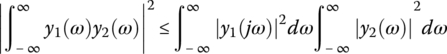
and the condition of equality holds if
where K is a constant and * denotes the complex conjugate. Now, if in Eq. 4.15 we assume that

then, one can write

Then, the maximum signal‐to‐noise ratio is given by the right side of Eq. 4.18. From Eq. 4.16, one can write for the transfer function that satisfies this condition:

Or the matched filter is given by

For a white noise, N(ω) is constant, and thus K/N(ω) is a constant gain factor that can be made unity for convenience. Then, by using the properties of Fourier transform, the matched filter impulse response is given by
This function is a mirror image of the input waveform, delayed by the measurement time T.
4.3.3 Optimum Noise Filter in the Absence of 1/f Noise
Figure 4.10 shows a detector system for the purpose of noise analysis. The detector is modeled as a current source, delivering charge Q˳ in a delta function‐like current pulse. The charge is delivered to the total capacitance at the preamplifier input, which is a parallel combination of the detector capacitance Cd, the preamplifier input capacitance Cin, and the effective capacitance due to preamplifier feedback capacitor, in the case of charge‐sensitive preamplifiers. This pulse at the preamplifier output, that is, pulse shaper input, can be approximated with a step pulse with amplitude Q˳/C. As it was shown in Chapter 3, the main component of noise at the output of a charge‐ or voltage‐sensitive preamplifier can be expressed as a combination of white, pink, and red noise that is dependent on frequency as f −2, f −1, and f 0, respectively. We initially assume that dielectric and 1/f noise are negligible. Then, the noise power density is given by

where constants a and b describe the series and parallel white noises. The noise power density can be written as

where

τc is called noise corner time constant and is defined as the inverse of the angular frequency at which the contribution of the series and parallel noise are equal. Irrespective of physical origin, the noise sources can be represented with a parallel resistance Rp and a series resistance Rs that generate the same amount of noise. One can easily show that τc = C(RpRs)0.5. Now by having the signal and noise properties, our aim is to use the matched filter concept for finding a filter that maximizes the signal‐to‐noise ratio. For a white noise, the matched filter is given by Eq. 4.21, but noise of Eq. 4.23 is not white. Therefore, we first convert the noise power density of Eq. 4.24 to a white noise. This procedure is shown in Figure 4.11. By passing the noise through a CR high‐pass filter with time constant τc, the noise power density becomes constant:


Figure 4.10 Equivalent circuit of a charge measurement system for deriving the optimum shaper. The original noise sources are at the input of a noiseless preamplifier followed by a noiseless shaper.

Figure 4.11 Finding the optimum filter by splitting the filtration into a whitening step and a matched filter.
This filter is called noise whitening filter. The detector pulse at the output of this filter is also an exponentially decaying pulse with a time constant equal to the noise corner time constant:
Now, by having a white noise at the output of the noise whitening filter, a second filter whose transfer function is chosen according to matched filter theory is used to maximize the signal‐to‐noise ratio. We already saw that the impulse response of such filter is the mirror image of the input pulse with respect to measurement time T. In our case, the input signal is the output of the noise whitening filter whose waveform is given by Eq. 4.26, and thus the matched filter is characterized with
By having the impulse response of the matched filter, the signal at its output is obtained as shown in Figure 4.12. The filter has a cusp shape with infinite length. This function implies an infinite delay between the event and the measurement time when the peak of the pulse is required. The signal‐to‐noise ratio defined as signal energy to noise mean‐square value depends on the measurement time of signal and is given by


Figure 4.12 The input and output of optimum filter. The output has a cusp shape with infinite length.
The maximum signal‐to‐noise ratio (ηmax) is obtained when T → ∞. From the previously mentioned relations, one can see that when τc = 0, that is, the noise becomes 1/f 2, no filtration is performed on the signal, which is understandable because signal and noise are of the same nature, and thus no filter can improve the signal‐to‐noise ratio. But when τc → ∞, the noise becomes white, and an arbitrary large signal‐to‐noise ratio can be achieved if a sufficiently long measurement time is available. The optimum cusp filter is of theoretical importance because it sets the upper limit to the achievable noise filtration, but it is not of practical importance due to its infinite length. However, it has been shown that by paying a small penalty on the noise performance, a cusp filter with finite width can be obtained [15], as shown in Figure 4.13a where it is the optimum filter for a pulse of fixed duration even if nonlinear and time‐variant systems are considered [16]. The finite cusp filter can be approximated with a triangular‐shaped pulse, and thus the triangular filter represents a noise performance close to finite cusp filter [17]. In spite of the desirable shape of the finite cusp filter for noise filtration and minimization of pulse pileup, its sharp peak makes it very sensitive to ballistic deficit effect. Therefore, a finite cusp filter with a flattop region, as shown in Figure 4.13b, has been suggested to make it immune to the ballistic deficit effect as well. A description of such filter can be found in Ref. [15].

Figure 4.13 (a) Finite cusp filter and (b) a finite cusp filter with a flattop region.
4.3.4 Optimal Filters in the Presence of 1/f Noise
In many spectroscopic systems, the contribution of 1/f noise to the total noise is insignificant, and the optimum filter described in the previous section can adequately describe the minimum noise level of the system. However, in some systems, the 1/f noise contribution is considerable, and thus in this section, we investigate the optimum filter when 1/f noise is present along with parallel and series white noises. From the discussion in Chapter 3, we know that the series 1/f noise and dielectric noise can be characterized with noise power density af/f and bf ω, respectively. When these noises along with the series and parallel white noises are converted into equivalent parallel current generators, the following noise power density is produced:

It is seen that the series 1/f noise, once transformed into an equivalent parallel noise, gives the same type of spectral contribution as the dielectric noise. By using the same definition of noise corner time constant as τc = C(a/b)0.5 and defining parameter K as

From Eq. 4.20 and by using Eq. 4.29, and performing some mathematical operations, one can determine the optimum filter in the time domain from the following integral [18]:
This integral can be done for different K values, and the results are illustratively shown in Figure 4.14a. The filters all have a cusp shape, while for K = 0, the filter becomes the classic cusp filter discussed in the previous section. The optimum filters in the presence of the 1/f noise decay to zero more slowly than the classic cusp filter (K = 0), and also the sharper slope of the pulses will produce more ballistic deficit problem. For practical purposes, filters with finite width have been analyzed, whose shape is illustrated in Figure 4.14b. A flattop region can be also added to this pulse to minimize the ballistic deficit effect. The effect of flattop region on the noise performance of filters is described in Ref. [19]. For optimum filter in presence of 1/f noise, one can calculate the optimum signal‐to‐noise ratio from Eq. 4.18 as


Figure 4.14 (a) The optimum filter in the presence of 1/f noise and (b) optimum filter with finite width.
The results of the integral are given by [18]


In addition to the white series and parallel noise and 1/f noise, in practice, other sources of noise such as parallel 1/f noise, Lorentzian noise, and so on may be present in a system. These cases have been extensively studied in the literature, and methods for the calculation of the optimum filter in the presence of arbitrary noise sources with time constraints have been developed. The detailed analysis of such filters can be found in Refs. [20–23].
4.3.5 Practical Pulse Shapers
We have so far discussed the optimum filters, irrespective of the way the filter is realized. However, the realization of optimal filters with analog electronics is usually difficult, and thus practical pulse shapers have been developed in response to the needs in actual measurements. In the following sections, we will discuss the most commonly used analog pulse shapers.
4.3.5.1 CR–RC Shaper
In the early 1940s, pulse shaping consisted essentially of a single CR differentiating circuit. It was then realized that limiting the high frequency response of the amplifier would reduce noise drastically, and this was achieved by means of an integrating RC circuit. The combination of the CR differentiator and RC integrator is referred to as a CR–RC shaper and constitutes the simplest concept for pulse shaping [24]. In principle, the time constant of the integration and differentiation stages can be different, but it has been shown that the best signal‐to‐noise ratio is achieved when the CR and RC time constants are equal [17]. The structure and step response of this simple band‐pass filter are shown in Figure 4.15, where the output shows a long tail that at high rates can cause baseline shift and pulse pileup problems, and for these reasons, this filter is rarely used in modern systems. The main advantage of this filter, apart from its simplicity, is its tolerance to ballistic deficit for a given peaking time that results from its low rate of curvature at the peak. In fact, the lower the rate of curvature at the peak of the step response of a pulse shaping network, the higher the immunity to the ballistic deficit [25].

Figure 4.15 (a) CR–RC pulse shaper and (b) its step pulse response.
4.3.5.2 CR‐(RC)n Shaping
A very simple way to reduce the width of output pulses from a CR–RC filter for the same peaking time is to use multiple integrators as shown in Figure 4.16. This filter is called CR–(RC)n filter and is composed of one differentiator and n integrators. The number of integrators n is called the order of the shaper. The transfer function of this filter is given by

where τ˳ is the RC time constant of the differentiator and integrators and Ash is the dc gain of the integrators. The transfer function contains n + 1 poles, where n is introduced by the integrators and one by the differentiator. The step response of the filter in time domain is given by

where A is the amplitude of the output pulse and τs = nτ˳ is the peaking time of the output. Figure 4.17 shows the step response of filters of different orders. As more integration stages are added to the filter, the output approaches to a symmetric shape and the width of pulses reduces, which is useful for minimizing the pileup effect. If infinitive number of integrators are used, a Gaussian shape pulse will be produced, but in practice only four stages of integration (n = 4) are considered, and the resulting CR–(RC)4 filter is called semi‐Gaussian filter. The choice of four integration stages is due to the fact that more integration stages will have a limited effect on the noise and shape of output pulses while it complicates the circuit design. In the design of CR–(RC)n filters, the most delicate technical problem is dc stability of the filter. Since the individual low‐pass elements are separated by buffer amplifiers, the dc gain can exceed the pulse gain, and thus a small input offset voltage will be sufficient to saturate the filter output. Therefore, ac coupling between stages may be used, but this is detrimental for the baseline stability as it was previously discussed.

Figure 4.16 Realization of a CR–(RC)n pulse shaper.

Figure 4.17 Step response of CR–(RC)n filters of different order.
A more practical approach to implement CR–(RC)n filters is to use first‐order active differentiator and integrator filters instead of passive RC and CR filters isolated by buffer amplifiers. Figure 4.18 shows active differentiator and integrator filters where op‐amps with resistor and capacitor feedbacks are used. For a first‐order active differentiator, one can easily show that the transfer function is given by
and the input–output relation in the time domain is given by

Figure 4.18 First‐order active differentiator and integrators.
It will be later shown that the differentiator is slightly modified to perform the pole‐zero cancellation as well. A first‐order active integrator is made by using a feedback network consisting of a parallel combination of a resistor and a capacitor with the transfer function
and the gain of the filter can be easily adjusted by resistor R2. A CR–(RC)n shaper is obtained by combining the active differentiator and several stages of integrators to obtain the desired symmetry of output pulses. By using the transfer functions of Eqs. 4.37 and 4.38, one can easily check that the resulting CR–(RC)n filter has a transfer function similar to that of classic ones.
4.3.5.3 Gaussian Shapers with Complex Conjugate Poles
As it was discussed earlier, a true Gaussian shaper requires an infinite number of integrator stages that is obviously impractical. However, a close approximation of a Gaussian shaper can be obtained by using active filters with complex conjugate poles. The properties of these filters were first analyzed by Ohkawa et al. [26]. The noise performance of such active filters is not necessarily superior to a CR–(RC)n network but can produce narrower pulses for the same peaking time and may be more economical in the number of components. Due to these reasons, such filters are the common choice in pulse shaping circuits. For a true Gaussian waveform of the form
The frequency characteristics of the waveform is given by
where A˳ is a constant and σ is the standard deviation of the Gaussian. According to Ohkawa analysis, if we assume the transfer function of the filter producing this waveform can be expressed in the form
where H˳ is a constant and Q(s) is a Hurwitz polynomial, then the problem of designing the Gaussian filter reduces to finding the best expression for Q(s). By using the relation H(jω)H(−jω) = [F(ω)]2 and from Eqs. 4.40 and 4.41, one can write

where s = jω. By a proper normalization, this equation can be written as
where p = σs. The Taylor expansion of this equation leads to
Now, Q(p) can be obtained by factorizing the right‐hand side of Eq. 4.44 into the same form as the left‐hand side. For example, for n = 1, the approximation results in
Therefore, Q(p) = 1 + p and the transfer function is given by
which is a first‐order low‐pass filter. For n = 2, one can write

The function Q(p) is then obtained as

and the transfer function that corresponds to Q(p) has conjugate pole pairs. For higher n values, the calculations are more complicated and require numerical analysis. From the previous discussion, we see that a good approximation of a Gaussian filter transfer function can be achieved by the introduction of complex conjugate poles to the filter. For realizing such filter, it is common to use a differentiator with a proper time constant, derived from the zero at the origin and a real pole, followed by active filter sections with complex conjugate poles. A second‐order low‐pass filter with two conjugate complex poles is used for this purpose, and higher‐order filters can be obtained by cascading an adequate number of the second‐order filter unit. For example, a Gaussian filter composed of the differentiator followed by two active filter sections corresponds to n = 5 and with three active filter sections corresponds to n = 7. The transfer function of active filters with complex conjugate pair poles is quite sensitive with respect to operational amplifier’s parameters, and thus there are only a few good‐natured designs producing stable waveforms over the complete range of shaping time constants, gain settings, temperature, counting rates, and so on. Figure 4.19 shows two topologies for realizing approximate Gaussian shapers with complex conjugate poles. The Laplace transform of the second‐order filter shown at the top of the figure can be written as [27]
where α = (R1 + R2)/R1 is kept low to quickly damp the output. The transfer function of the second‐order active filter shown in the bottom of Figure 4.19 is also given by


Figure 4.19 Two examples of second‐order active integrators for realizing Gaussian shapers.
The gain of this filter is easily adjusted by the coupling resistor R3. Other examples of such filters will be described in Section 4.6.3.
4.3.5.4 Bipolar Shapers
If a differentiation stage is added to the output a CR–(RC)n or active shapers, a bipolar pulse is produced. Such shaper has a degraded noise performance compared with monopolar filters but in some situation is preferred because monopolar shapers at high rates lead to a baseline shift, which can be reduced by a bipolar shape. As already mentioned, baseline shift is mainly because a CR coupling can transmit no dc and thus pulses with undershoot are produced. A bipolar pulse having an area balance between positive and negative lobes results in no dc component, and thus no baseline shift would be produced. Figure 4.20 shows a bipolar pulse and a monopolar pulse of the same peaking time. The bipolar pulse shows a longer duration than the monopolar pulse, which is not desirable from pulse pileup point of view. For the same overall pulse length, the peak of a bipolar pulse would also have a smaller region of approximate flatness than in unipolar pulse and so would have a larger ballistic deficit. Therefore, in many situations, a truly unipolar pulse together with a baseline restorer may be preferred to bipolar pulses.

Figure 4.20 A comparison of a bipolar and monopolar pulse of the same peaking time.
4.3.5.5 Delay‐Line Pulse Shaping
Delay‐line amplifiers are used in applications where noise performance is not of primary importance. These filters can produce short duration pulses and thus less sensitive pulse pileup effect. Figure 4.21 shows the block diagram of a delay‐line shaper. The output has a rectangular shape whose width is Td. It is clear that the pulse has a quick return to baseline, which is very important in terms of count rate. Delay‐line shapers are also immune to ballistic deficit effect, but the noise performance of this filter is not very good because this shaper does not place a limit on the high frequency noise and the cutoff frequency is determined by the physical parameters of the system [28]. The transfer function of the filter is given by

Figure 4.21 A block diagram of delay‐line pulse shaper.
For a white input noise, the output noise in the frequency interval up to ωf is given by

where N˳ is the white noise power spectrum. From Eq. 4.52, it follows that at high frequencies, the output noise approaches to 2Nωh. Such noise behavior is also valid for other noise spectra, which limits its applications in high resolution measurements but still useful for spectroscopy applications with scintillation detectors in which the electronic noise does not play a major role. If a second delay‐line stage with the same delay is added to the shaper, a bipolar pulse is produced and the shaper is called double delay‐line shaping. Such shaper is very useful for pulse counting, pulse timing, and pulse‐shape discrimination applications as well.
4.3.5.6 Triangular and Trapezoidal Shaping
It was already mentioned that a triangular filter represents a noise performance close to that of finite cusp filter. A trapezoidal filter can be realized by integrating the output of a suitably double delay‐line‐shaped pulse. The noise performance of doubly delay‐line shaper at high frequency is poor, but as a result of the integration of the noise performance, the resulting triangular‐shaped pulse significantly improves. However, the sensitivity of the triangular‐shaped pulse to the ballistic deficit effect still remains. Trapezoidal filters were introduced to address the sensitivity to ballistic deficit effect of triangular filters by adding a flattop region to the pulses [29, 30]. A method of transforming preamplifier pulses to a trapezoidal‐shaped signal is shown in Figure 4.22. For a steplike input pulse, a rectangular pulse is produced at the output of the first delay‐line circuit, which is then again fed to a delay‐line circuit with a proper amount of delay to produce a double delay‐line‐shaped pulse. Finally, by integrating this pulse with an integrator, a trapezoidal pulse shape will be produced. The response of a trapezoidal filter to input pulses of different risetimes is shown in Figure 4.23. The time scale of the filter is determined by two parameters: a flattop region that helps a user to minimize the ballistic deficit effect and a risetime to minimize the effect of noise. If the flattop region is long enough, it can completely remove the ballistic deficit effect, but it increases the noise and thus should not be chosen unnecessarily long. A trapezoidal filter also addresses the pulse pileup effect by the fact that the pulse quickly returns to the baseline, and thus the system becomes ready to accept a new pulse, while in semi‐Gaussian filters, longer times are required for a pulse to return to the baseline, risking a pulse pileup. In principle, a trapezoidal filter is very suitable for the high rate operation of large germanium detectors where long and variable shape pulses are to be processed. However, this filter has not been widely used in analog pulse processing systems due to the practical problems in the accurate realization of the transfer function that stem from high frequency effects in operational amplifiers, exponential decay preamplifier pulse, and imperfections in the delay‐line circuits. But this filter is readily implemented in digital domain and its excellent performance has been well demonstrated.

Figure 4.22 A block diagram of trapezoidal filter circuit.

Figure 4.23 Trapezoidal filter output for inputs of different risetime.
4.3.5.7 Time‐Variant Shapers, Gated Integrator
The pulse shapers discussed so far are called time invariant, which means that the shaper performs the same operation on the input pulses at all times. Another class of shapers used for nuclear and particle detector pulse processing are time‐variant shapers in which the circuit elements switch in synchronism with the input signals. In theory, time‐variant shapers do not allow better noise performance than the best time‐invariant shapers, but practically in some applications, they offer much better performance when low noise, high count rate capability, and insensitivity to ballistic deficit effect are simultaneously required. One of the most important time‐variant shapers used in nuclear spectroscopy is gated integrator, described by Radeka [31, 32]. The block diagram of a gated integrator is shown in Figure 4.24. It consists of a time‐invariant prefilter and the time‐variant integration section. By detecting the start of a signal in a parallel fast channel, switch S1 is closed and switch S2 is opened so that the feedback capacitor acts as an integrator for the output of prefilter. At the end of prefilter signal, switch S1 is opened and thus the integration is stopped. Switch S2 is left open for a short readout time, following the opening of S1 that leads to a flattoped output signal. Since the integration time extends beyond the charge collection time in the detector, the sensitivity to ballistic deficit is significantly suppressed. The shape of the impulse response from the prefilter determines the noise performance of the gated integrator, and it has been theoretically shown that the optimum prefilter impulse response would be rectangular in shape [32]. Such impulse response can be produced by delay‐line circuits, but delay‐lines do not have the needed stability for high quality spectroscopy, and thus, semi‐Gaussian shapers are generally used as prefilters in commercial gated integrators. Figure 4.25 shows the waveforms for a gated integrator with semi‐Gaussian prefilter when it is fed with a semiconductor detector pulse. The input pulse from the preamplifier has a small electron component followed with a long hole component. As the shaping time constant of the semi‐Gaussian filter is chosen to minimize noise, a long tail on the pulse is produced due to the incomplete processing of the detector pulse, and thus at this stage the ballistic deficit effect is significant. Nevertheless, in the next stage, the pulse is integrated for a time beyond the charge collection time, and thus the ballistic deficit effect is perfectly removed. A different type of prefilter that produces lower noise and less sensitivity to low frequency baseline fluctuations is described in Ref. [33].

Figure 4.24 Block diagram of gated integrator.
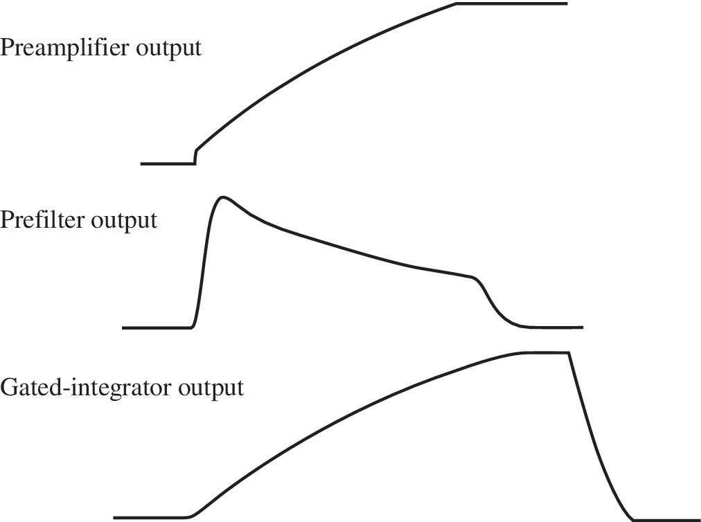
Figure 4.25 The signal waveforms at different stages of a gated integrator with semi‐Gaussian prefilter when it is fed with a pulse from a semiconductor detector.
As shown in Ref. [34], the maximum available signal‐to‐noise ratio for the time‐variant shapers is the same as for the time‐invariant shapers, but, in some detectors, particularly large coaxial germanium detectors and planar compound semiconductor detectors such as TlBr and HgI2, the risetime variations in detector signals may become very significant, and consequently energy resolution is limited by the ballistic deficit effect unless a shaper with large time constant, at least equal to the maximum detector signal risetime, is used. This however produces a large low frequency noise. A gated integrator minimizes the effect of noise during the prefiltration process and solves the ballistic deficit problem by integrating the entire output pulse of the prefilter. Moreover, time‐variant shapers offer the advantage of immunity to pulse pileup by the fast and tail‐free recovery to the baseline at the end of the shaped pulses.
4.3.6 Noise Analysis of Pulse Shapers
4.3.6.1 ENC Calculations
The ENC is a common measure of the noise performance of nuclear charge measuring systems. It includes the effects of all physical noise sources, the capacitances present at the preamplifier input, the time scale of the measurement, and the type of the shaper. An equivalent circuit for ENC calculation is shown in Figure 4.26. By definition, the ENC is the charge delivered by the source to the total capacitance that produces a voltage pulse at the shaper output whose amplitude is equal to root‐mean‐square value of noise (vrms). In general, the ENC can be expressed as
where C is the total capacitance at the input and G is the gain of shaper. It is clear that achieving a low ENC value requires to minimize the input capacitances, particularly parasitic capacitance at the input. For an ideal charge‐sensitive preamplifier, the output is given by Q/Cf, and by assuming unity gain for the shaper, one can write

Figure 4.26 An equivalent circuit for the calculation of the equivalent noise charge.
The vrms value of noise is calculated from

where vo is the noise voltage at the preamplifier output, and its power density can be written as (Eq. 4.64)

One should note that in these calculations, the spectral noise densities are considered to be mathematical ones, defined on the (−∞, ∞). The mean‐square value of noise is calculated with

As it is shown in Ref. [35], by using the normalized frequency x = ωτ, Eq. 4.57 can be rewritten as

where τ is the time width parameter of the shaper, either the peaking time of the step pulse input or some other characteristic time constant of the shaper. The integrals in this equation can be expressed as


The three parameters A1, A2, and A3 are called shape factors for white series, 1/f, and white parallel noise and depend on the type of the shaper. The A1 and A3 coefficients can be also calculated in the time domain by using Parseval’s theorem. From Eq. 4.55, the ENC2 is finally given by

ENC 2 is therefore expressed through the total capacitance, the four parameters a, af, b, and bf that describe the input noise sources, the shaping time constant of the shaper, and the shaper characteristics. This relation is a general relation for all semiconductor charge measuring systems including scintillation detectors coupled to photodiodes and avalanche photodiodes. One should note that in the previously mentioned relation, the voltage and current noise densities are half of mathematical noise densities as the integrations were performed from −∞ to ∞. As an example, we calculate the A1 coefficient for a triangular shaper. The impulse response and transfer function of triangular shaper are given by

and
From Eq. 4.59, one can calculate A1 as

The shape factors for some of the common filters are given in Table 4.1 [19].
Table 4.1 The shape factors for some of the common filters.
| Shaper | A1 | A2 | A3 |
| Infinite cusp | 1 | 0.64 | 1 |
| Triangular | 2 | 0.88 | 0.67 |
| Trapezoidal | 2 | 1.38 | 1.67 |
| CR–RC | 1.85 | 1.18 | 1.85 |
| CR–(RC)4 | 0.51 | 1.04 | 3.58 |
4.3.6.2 ENC Analysis of a Spectroscopy System
The ENC can be split into its components as
where ENCs, ENCp, and ENC1/f are the contributions due to the white series, white parallel, and 1/f noise, respectively. The variation of the ENC with a typical filter’s time constant is illustratively shown in Figure 4.27. In Figure 4.27a, it is shown that there is a shaping time at which the noise is minimum. This shaping time is called the noise corner and is given by [35]


Figure 4.27 (a) Variations of ENC and its components with shaper’s time constant. (b) The effect of increase in series noise on the location of noise corner and (c) the effect of parallel noise on the location of noise corner.
The noise corner is independent of 1/f noise and at this shaping time, ENCs = ENCp. It is also apparent that the series white noise decreases with the filter’s time constant, while the parallel noise increases with the filter’s time constant. The ENC1/f, resulted from dielectric noise and series 1/f noise, does not change with the shaper time constant, and it is only weakly dependent on the type of shaper [35]. Figure 4.27b and c shows that by increasing the series white noise, the noise corner shifts to larger time constants, while by increasing the parallel noise, the noise corner shifts to smaller time constants.
The contributions from white series, white parallel, and 1/f noise in Eq. 4.60 can be further split to their components. For example, in a charge‐sensitive preamplifier system, the main contribution to series white noise is due to the FET transistor thermal noise whose corresponding ENC can be obtained by replacing a in Eq. 4.60 from Eq. 3.45 as

where q is the electron charge and converts the ENC from coulomb to the number of electrons (e− rms). In this relation, a factor 1/2 is considered to account for the physical noise power density. By substituting for the transconductance from Eq. 3.13, one obtains

By using the mismatch factor m = Cd/Cin, the ENCth is written as

As it was mentioned before, the minimum thermal noise is achieved by capacitive matching (m = 1), and the deviation from the minimum value can be determined from

where ENCmin is the ENCth under capacitive matching. The ENCs due to other physical noise sources in a detector–preamplifier system can be found in Refs. [14, 36, 37].
4.3.6.3 ENC Measurement
Figure 4.28 shows an arrangement suitable for the measurement of ENC of a spectroscopy system. A charge‐sensitive preamplifier and a pulse shaper are employed in the setup, and the output noise is measured by an output analyzer that can be a wideband rms voltmeter or an MCA. The detector’s pulses are modeled with a precision pulse generator that injects steplike voltages that carry a signal charge Q = VCtest at the preamplifier input through the test capacitance Ctest. By having the rms value or FWHM of pulse‐height spectrum, Eq. 4.3 can be then used to determine the ENC. The measured ENC is the total ENC described by Eq. 4.60, and the test capacitance should be added to the other capacitances at the input so that Ctot = Cd + Cin + Cf + Cs + Ctest. The different components of the ENC can be also extracted by measuring the ENC as a function of shaping time constant and fitting a function of the following type on the data [38, 39]:
where H1, H2, and H3 are the fitting parameters that determine the series, parallel, and 1/f noise, respectively.

Figure 4.28 An experimental arrangement for ENC measurement.
4.3.6.4 Noise Analysis in Time Domain
A time‐invariant shaper is completely described by its transfer function, and thus the frequency domain techniques can be conveniently used for calculating the noise performance of the shapers. However, for time‐variant shapers, the frequency domain methods are not strictly valid or cannot be easily used. Nevertheless, the noise analysis of both time‐variant and time‐invariant shapers can be carried out in the time domain with the advantage that better intuitive judgments about the effects of shaping can be made [40–42]. The noise analysis in time domain is illustrated in Figure 4.29. In the upper part of the figure, the series and parallel white noise sources are shown that are considered to result from individual electrons that occur randomly in time. The random charge impulses from parallel current noise generator are integrated on the total input capacitance, producing input step voltage pulses. This noise is referred to as step noise, which is processed with the shaper exactly the same as detector pulses that also appear as a step pulse with amplitude Q/C at the shaper input. On the other hand, the series noise is independent of the capacitance C and remains as a random train of voltage impulses at the shaper input. This noise is called delta noise. The time domain noise model deals only with the two white noise sources because 1/f noise cannot be represented so simply. The noise waveforms at the input of the shaper are shown in the lower part of Figure 4.29. The individual step and delta noise pulses at the output of the shaper are superimposed together to determine the noise at a measurement time T. Since the shaper affects the step and delta noises differently, two noise indexes are used to describe the performance of a shaper. These are the mean‐square value of the shaper output due to the all noise elements preceding the measurement time. For step noise index, each noise pulse occurring at a time t before the measurement time T leaves a residual F(t) at the measurement time. This residual function is called weighting function and is a property of the shaper. According to Campbell’s theorem, the mean‐square effect of fluctuations in these contributions at the measurement time is obtained by summing the mean‐square values of the noise residuals for all time elements preceding the measurement time. Thus, the step noise index is given by [40, 41]
where S is the signal peak amplitude for a step input pulse. For delta noise, the noise index calculation is equivalent to apply impulses at the input that produce residual proportional to F′(t). The noise index for the delta noise is given by [40, 41]

Figure 4.29 Noise analysis in time domain.
The weighting function for time‐invariant systems is simply the step pulse response. As an example, we calculate the noise indexes of a simple CR–RC shaper. From Eq. 4.35, the step response of the shaper normalized to unity peak amplitude is given by
Thus,


The noise indexes can be used to compare the performance of different shapers in regard to step and delta noises, that is, series and parallel white noises. For example, for a triangular shaper with the risetime τ, the step and delta noise indexes are, respectively, 0.67/τ and 2/τ, which indicate the better performance of the triangular filter in regard to step noise. For a time‐variant system, the weighting function is generally quite different from its step response, and the shaping of noise pulses is determined based on their time relationship to the signal. A calculation of noise indexes for various time‐variant and time‐invariant pulse shapers can be found in Ref. [40].
4.3.7 Pole‐Zero Cancellation
We have so far described a linear amplifier/shaper from noise filtration point of view. In addition to pulse shaping network, an amplifier is generally equipped with circuits that aim to minimize the other sources of fluctuations in the amplitude of the pulses. One of these circuits is pole‐zero cancellation circuit and lies at the amplifier input. The output pulse of a charge‐ or voltage‐sensitive preamplifier normally has a long decay time constant. When such decaying pulse is fed into an amplifier circuit, the differentiation of the pulse produces an undershoot. Consequently, at medium to high counting rate, a substantial fraction of the amplifier output pulses may ride on the undershoot from a previous pulse, and this can seriously affect the energy resolution. The production of the undershoot is explained by expressing the preamplifier pulse in Laplace domain with V(s) = τ˳/(1 + sτ˳) where τ˳ is the decay time constant of the pulse and by using the transfer function of the differentiator with time constant τ as HCR = sτ/(1 + s). The differentiator output is given by
The presence of two poles means that this pulse is a bipolar one and thus it exhibits undershoot. A pole‐zero cancellation circuit removes the undershoot. This procedure is shown in Figure 4.30 where the simple upper CR circuit is replaced with the lower circuit in which an adjustable resistor R1 is added across the capacitor C. The transfer function of modified differentiator is given by

where τ1 = R1C and τ2 = (R1‖R)C. If the value of R1 is chosen so that τ1 = τ˳, then the pole of the circuit is cancelled by the zero and again an exponentially decaying pulse with decay time constant of τ2 is obtained:

Figure 4.30 Basic pole‐zero cancellation circuit.
Figure 4.31 shows the waveforms before and after the pole‐zero cancellation. Virtually all spectroscopy amplifiers incorporate pole‐zero cancellation feature, and its exact adjustment is critical for achieving good resolution at high counting rates. A more practical pole‐zero cancellation circuit is shown in Figure 4.32. In this configuration, the pole‐zero cancellation is achieved exactly the same as that in the clipping network of preamplifier discussed in Section 3.2.6.1. This configuration allows to adjust the desirable gain through the feedback resistor. A more sophisticated circuit for pole‐zero cancellation is reported in Ref. [43].

Figure 4.31 The preamplifier pulse and waveforms before and after pole‐zero cancellation.

Figure 4.32 A common pole‐zero cancellation circuit used in shaping amplifiers.
4.3.8 Baseline Restoration
As it was discussed in Section 4.2.2.3, in ac coupling of the amplifier and ADC, the use of monopolar pulses can lead to baseline fluctuations. Although the use of bipolar pulses can alleviate this problem, in many applications, a bipolar shape involves a nonacceptable degradation in the signal‐to‐noise performance and a long‐lasting negative tail that increases the probability of pileup between signals. Therefore, in most situations, a unipolar shaping is preferred, and a circuit called baseline restorer is adopted at the amplifier output to reduce the baseline shift. The baseline restorer also reduces the effect of low frequency disturbances, like hum and microphonic noise, which make it useful even in a completely dc‐coupled system. The functional principle of most of the generally used baseline restorers is illustrated in Figure 4.33. The basic components of the restorer are the capacitor and the switch. The resistor R indicates that the switch is not perfect. When a pulse arrives, the switch is opened and the switch is closed as soon as the signal vanishes. Therefore, in the presence of pulses, the restorer acts as differentiator with a very long time constant because the subsequent circuit has a very high input impedance. As a result of the large time constant, both baseline shift and pulse undershoot associated with ac coupling will be avoided. As soon as the positive part of the pulse is over, the switch S closes and the time constant of the differentiator turns to a small value. The negative tail of the pulse, therefore, recovers quickly to zero, and the original negative tail of the pulse is transformed into a short tail, and also low frequency variations in the baseline are strongly attenuated. The switch control is based on the detection of the arrival of pulses. The choice of the time constant CR is a very important aspect in the optimization of the performances of a baseline restorer. A small CR time constant results in a more effective filter for the low frequency baseline fluctuations and a faster tail recovery after the pulse, but it increases the high frequency noise, and thus the choice of CR is generally a compromise. The first baseline restorers, based on the diagram shown in Figure 4.33, were proposed by Robinson [44] and by Chase and Poulo [45] in which diode circuits are used to transmit the pulses and short‐circuit the pulse tails to ground. They are effective in reducing baseline shifts and have a compact schematic, but they have non‐negligible undershoot and also distort low amplitude pulses. These shortcomings have been addressed in modern baseline restoration circuits whose details can be found in Refs. [46–48].

Figure 4.33 Principle of baseline restorer.
4.3.9 Pileup Rejector
Amplifiers are usually equipped with a circuit to detect and reject the pileup events. Figure 4.34 illustrates a common method of pileup detection [49]. In parallel to the main pulse shaping channel or slow channel, the preamplifier output pulses are processed in a fast pulse processing channel in which pulses are strongly differentiated to produce very narrow pulses. The narrow width of the pulses enables one to separate pileup events though the noise level is larger than that in the main spectroscopy channel. The output of the fast channel is then used to produce logic pulses that trigger an inspection interval covering the duration of the pulses from the slow channel. The detection of pileup events is based on the detection of a second logic pulse during the inspection interval, and if this happens, the output of the main pulse shaping channel is rejected. This pileup detection method performs well for pulses of sufficiently large amplitude, but its performance is limited for low amplitude pulses that can lie below the discrimination level of producing logic pulses and also for pileup pulses with very small time spacing. There have been several other methods for the detection of pileup events; some of them are described in Refs. [50, 51].

Figure 4.34 Pulse pileup detection.
4.3.10 Ballistic Deficit Correction
In principle, the minimization of ballistic deficit effect in time‐invariant pulse shapers requires to increase the time scale of the pulse shaper. Since this is not always possible due to the effects of noise and pulse pileup, there have been some efforts to correct this effect at the shaper output. A correction method proposed by Goulding and Landis [52] is based on the relationship between the amplitude deficit and the time delay ΔT in the peaking time of the pulse:

where V˳ is the peak amplitude of the output signal for a step function input, ΔV is the ballistic deficit, T˳ is the peaking time of the output signal for a step function input, and ΔT is the delay in the peaking time for a finite risetime input. By having the amount of ballistic deficit, a correction signal is added to the output pulse from the linear amplifier to obtain the true pulse amplitude. This approach also compensates for the deterioration of the energy resolution caused by charge‐trapping effects. Another method of ballistic deficit compensation is based on using two pulse shaping circuits having different peaking times [53]. The correction factor is decided based on the difference in the output of shapers and is then added to the output signal of the shaping channel with larger time constant.
4.4 Pulse Amplitude Analysis
4.4.1 Pulse‐Height Discriminators
The selection of events that lie in an energy range of interest is performed by using pulse‐height discrimination circuits. Such devices produce a logic output pulse when an event of interest is detected. Figure 4.35a shows the operation of a discriminator that selects the events whose amplitude lies above a threshold level, for example, above the noise level. Such discriminator is called integral discriminator and can be built by using an analog comparator, while the discrimination level can be varied over the whole range of pulse amplitudes [17]. Figure 4.35b shows the operation of a discriminator that produces an output logic pulse for pulses whose height lie within a voltage range. Such discriminators are called SCA that were already introduced at the beginning of this chapter. An SCA contains LLD and ULD that form a window of the width ΔE, which is called energy window or “channel.” The block diagram of an SCA is shown in Figure 4.36. It is basically composed of two comparators that allow the adjustment of the LLD and ULD of SCA and an anticoincidence logic circuit that produces an output logic pulse if it receives logic pulses from one of the comparators. The output of an integral discriminator can be produced before the pulse reaches its maximum value, but the output logic pulse from an SCA must be produced after the input pulse reaches its maximum amplitude, while the SCA logic circuitry also needs some time to produce the output logic pulse. The timing relation of the output logic pulse with the arrival time of the input analog pulse is important in many applications, and thus commercial SCAs are classified into two basic types: non‐timing and timing SCAs. In non‐timing units, the SCA output pulse is not precisely correlated to the arrival time of the input pulses, but for timing SCAs output logic pulses are precisely related in time to the occurrence of the event being measured. In addition to simple counting applications, the timing SCAs are used for coincidence measurement, pulse‐shape discrimination, and other applications where the precise time of occurrence is important, which will be discussed in the next chapters. Some designs of SCA circuits can be found in Refs. [54–56]

Figure 4.35 (a) Operation of an integral discriminator and (b) differential discriminator or SCA.

Figure 4.36 Basics of an SCA.
4.4.2 Linear Gates
In many applications, some criteria are imposed on pulses before performing an amplitude analysis on them. Such criteria might include setting upper and lower amplitude limits, requiring coincidence with signals in the other measurement channels, and so on. A linear gate is a circuit that is used for this purpose by letting analog pulses of interest to pass on to a subsequent instrument for further analysis while blocking the other pulses. In such circuits, the transmission or block of analog pulses is controlled by applying a logic pulse at a control input. The use of a logic pulse in blocking or passing the analog signal can be in different ways. Figure 4.37 shows two ways of the operation of a linear gate. In the upper part of the figure, the input analog signal is transmitted to the output if it is accompanied with a logic pulse; otherwise, the output is attenuated. In the lower part, linear gate blocks a signal if it is accompanied with a logic pulse. One should note that the logic pulse must be sufficiently long to cover the whole duration of analog pulse. There are many ways to implement linear gates, and a variety of circuits have been devised for this purpose such as diode bridges and bipolar and FET transistors whose details can be found in Refs. [17, 27, 57]. The linearity, stability, pedestal level, and transients during the switching times are among the important parameters of a linear gate.

Figure 4.37 Two ways of operating linear gates. In the upper part, a linear gate transmits a signal when it is accompanied with a logic pulse. In the lower part, linear gate blocks the signal if it is accompanied with a logic pulse.
4.4.3 Peak Stretcher
The measurement of the amplitude of an amplifier output pulses by an ADC generally takes a longer time than the duration of the pulse signal. Thus before starting the pulse‐height measurement, one needs to stretch the input signal in order to store the analog information at the input of ADC for a length comparable with the conversion time of the ADC. This function is achieved by using circuits called pulse stretcher or peak detect sample and hold circuits, which are based on using a capacitor as a storage device for pulse amplitude [17]. Figure 4.38 shows a simplified diagram of such circuits. An operational transconductance amplifier is usually employed to serve as the charging current source. When the input voltage is higher than the output voltage, the current from operational amplifier charges the storage capacitor, while the diode is in conduction. Once the input voltage is lower than the output voltage, the hold capacitor cannot be discharged as the diode is in reverse bias, and thus it holds the maximum value of the input. In practice, due to the presence of leaks in the circuit and imperfections in the storage capacitor, the output voltage may reduce during the holding time, and thus compensation currents are introduced to maintain the precision of the output amplitude [58–60].

Figure 4.38 Simplified peak stretcher circuit.
4.4.4 Peak‐Sensing ADCs
The ADCs intended for use in classic MCAs produce only a single digital output value that represents the pulse amplitude, and such ADCs are called peak‐sensing ADC. In other situations, analog‐to‐digital conversion can be continuously performed on a signal to obtain the complete signal waveform, and these types of ADC are called free‐running ADCs. One other type of ADC is charge‐integrating ADCs, which is used with current generating devices such as PMTs. In this section, we focus on peak‐sensing ADCs used in classic MCAs. The performance characteristics of MCAs, number of channels, linearity, and dead time are normally dependent on the specifications of the peak‐sensing ADC. The basic operation of an ADC is illustrated in Figure 4.39. The input range from Vmin to Vmax is ideally divided into N channels of equal width Δ:
where N is the number of channels and is usually an integer power of two so that it can be expressed as N = 2k where k refers to the number of bits. The channels are numbered from Vmin to Vmax so that the channel defined by the boundaries Vmin and Vmin + Δ is conventionally labeled channel number zero and that by the boundaries Vmin + NΔ is the channel number N − 1. The resolving capability of ADC indicates that an ADC is able to resolve two amplitudes as long as their difference is greater than Δ. For example, in an 8‐bit ADC with an input range of 0–10 V, the number of channels is 28 = 512, and each channel width is 10 V/512 = 0.01 V. This is equal to the minimum change in the pulse amplitude to generate a change in the ADC binary output and is called the least significant bit (LSB). A k bit ADC produces a string of k ones or zeros, and the first converted digital bit is called the most significant bit (MSB). The number of the channels is generally decided based on the energy resolution of the detector and the requirements of the measurement. By increasing the number of channels, larger statistical fluctuations result because a lower number of counts per channel will be collected in a given time from a given spectrum of interest due to the smaller width of channels. The need of ADCs with high resolution depends on the resolution of the detector. In an ideal system, all the channels should have equal width though in practical systems the channel width may vary. The nonuniformities in the width of channels are called differential nonlinearity. Another parameter of an ADC is its integral nonlinearity. ADCs for spectrometric applications, especially if they are intended to operate over a wide input range, should have an adequately high degree of integral linearity. The integral nonlinearity can be measured with a precision pulser: a calibration line is obtained by fitting a linear function on the measurements of the channel number versus the input pulse amplitude. The integral nonlinearity is given by the maximum deviation of the measured curve from the fitted line expressed as percentage of full scale. For example, a 12‐bit ADC featuring 0.1% integral has a real behavior that deviates from the reference straight line by four channels. The speed of ADC is another important feature that determines the dead time of the pulse‐height measurement system and depends on ADC’s principle of operation. Three types of ADCs have been used in classic MCAs: the Wilkinson‐type ADC, the successive‐approximation (SA) ADC, and flash ADC, among which the Wilkinson‐ and SA‐type ADCs are the most widely used.

Figure 4.39 The operation of a peak‐sensing ADC.
4.4.4.1 Wilkinson‐Type ADC
The Wilkinson ADC was introduced in 1950 [61] and its operation is illustrated in Figure 4.40. It involves stretching the signal pulse on a storage capacitor so that the pulse is held at its maximum value. Then, a high precision constant current source is connected to the capacitor, which is disconnected from the input, to cause a linear discharge of the capacitor voltage. At the same time, a clock starts and a counter counts the clock pulses for the duration of the capacitor discharge, that is, until the voltage on the capacitor reaches zero or a reference low voltage. Since the time for linear discharge of the capacitor is proportional to the original pulse amplitude, the number recorded in the address counter (N) reflects the pulse amplitude. An alternative arrangement for Wilkinson‐type ADC is to charge up a second capacitor with a constant current until its voltage reaches that of input pulse height. Simultaneously, a linear ramp is made to run from zero to the pulse amplitude, and the time taken by the ramp is measured by counting the number of clock pulses during the ramp. In either case, the time taken by a Wilkinson ADC to convert the pulse amplitude depends on the clock frequency fc and the channel number N. The total conversion time in an MCA is the sum of the discharging time and the time needed to store the result of conversion in the memory, which is usually one order of magnitude shorter than the discharge time (from 0.5 to 2 µs). Although the discharge time can be reduced by increasing the discharge current, to achieve good resolution and short discharging time, the clock frequency must be then increased, which is limited by the available technology to 400 MHz. The advantage of Wilkinson ADCs is low differential nonlinearity (typically <1%), which is due to the exceptional stability achievable in electronic oscillators. The disadvantages are the long conversion time and its dependence on pulse amplitude that leads to long dead times.

Figure 4.40 Principle of a Wilkinson‐type ADC.
4.4.4.2 The Successive‐Approximation ADC
The block diagram of a standard SA ADC is illustrated in Figure 4.41. It consists of three components: a comparator, a digital‐to‐analog converter (DAC), and a digital control block that can be a register. This arrangement finds the value of the input signal by doing a so‐called binary search. A peak‐hold circuit delivers the maximum of the input signal to the comparator, so the input signal has a fixed value within the conversion time. In the start of the binary search, the input to the DAC is set to the digital value that is half the ADC output range, and the comparator compares the input signal with the DAC signal. If the input signal is larger than the DAC value, the MSB stays on 1; otherwise it is turned off. Then, the next bit of the DAC is switched on and the same test is done. This process is repeated until all bits have been tested. The bit pattern set in the register driving the DAC at the end of the test is a digital representation of the analog input pulse amplitude. If the ADC has k bits (2k channels), k test cycles are required to complete the analysis. In an SA ADC, the conversion time is the same for all pulse amplitudes, which improves the overall conversion time compared with Wilkinson‐type ADCs. However, the differential nonlinearity of these ADCs is not adequate. This problem is overcome by adding the sliding scale linearization that was introduced by Gatti and coworkers [62]. The sliding scale method is described in Figure 4.42, which is based on the averaging effect that is obtained by summing an auxiliary random analog signal to the ADC input whose digital representation is then subtracted from the ADC output after conversion in order to obtain true digital representation of the input. The result of this process is the statistical equalization of the channels width, thus improving differential nonlinearity. The SA ADC with sliding scale linearization exhibits low differential nonlinearity (<1%) and a short conversion time (2–20 µs) that is independent of the pulse amplitude. A drawback of this approach is that for a sliding scale of M bits, 2M − 1 channels are lost, and thus methods have been developed to exploit the lost channels [63, 64].
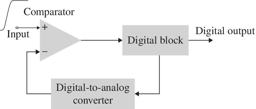
Figure 4.41 The block diagram of a successive‐approximation ADC.

Figure 4.42 Block diagram of successive‐approximation ADC with standard sliding scale linearization.
4.4.4.3 The Flash ADC
Figure 4.43 depicts the principle of the flash ADC. The ADC is constructed by stacking a series of comparators so that each comparator’s threshold is a constant increment in voltage ΔV above the previous threshold. In this way, each comparator compares the input signal to a unique reference voltage. As the analog input voltage exceeds the reference voltage at each comparator, the comparator outputs will sequentially saturate to a high state. The outputs of the comparators are fed into the digital output encoder that produces a binary output. A k bit ADC requires 2k − 1 comparators, and thus the number of comparators rapidly increases with the resolution of ADC. The advantage of flash ADCs is its speed so that conversion times are in the nanosecond range. The disadvantage is large differential nonlinearity, which limited its use in classic MCAs. However, it was the outcome of flash ADC with conversion times of a few nanoseconds that finally led to architectural changes in pulse spectrometry systems, allowing its evolution toward the full digital systems.

Figure 4.43 Block diagram of a flash ADC.
4.4.5 Multichannel Pulse‐Height Analyzer
The structure of a classic MCA is shown in Figure 4.44. First, a linear gate that is controlled by an SCA selects the pulses that lie in the input range of interest. The LLD level of SCA is normally adjusted to prevent the noise events from entering the system as it wastes the ADC time on the analysis of noise signals, while the ULD of SCA is adjusted to prevent the ADC from wasting time converting signals outside the range of allocated memory. The linear gate may be also operated with external logic pulses when it is needed to impose other criteria on the pulses. A peak stretcher prepares the pulses transmitted by the linear gate to be processed by the ADC. The gate at the input of the ADC is initially open, and it closes as soon as the maximum amplitude is captured by the pulse stretcher. This is to protect the ADC output against contamination from succeeding pulses. During the time that this gate is closed, the system is unable to accept new pulses, and this is the major source of dead time in an MCA. After the ADC converts the maximum pulse height to a digital output, the binary output is sent to a histogramming memory. If the pulse falls in the Nth channel, one count is added to the existing counts in the Nth memory location of the histogramming memory. Once the analysis of the pulse is completed, the MCA opens its linear gate and waits for the next available pulse to arrive. The process is repeated on a pulse‐by‐pulse basis over the counting time established by the experimenter. At the end of the counting time, the histogramming memory contains a record of counts versus memory location that can be displayed to present the energy spectrum through a calibration of channel number versus particles energy. The MCAs are generally equipped with a live time clock that provides the time during which the MCA has been receptive to incoming pulses (live time) and the fraction of time the gate is closed (dead time). The live time operation of an MCA is usually satisfactory for making routine dead‐time corrections in order to calculate the count rate of incoming events. However, at high count rates, the simple built‐in live time clock will not be accurate, and thus different methods have been developed to separately determine the dead time of the system. One should note that errors may be introduced by the correction methods, and thus the best way is to operate the system under low dead times.

Figure 4.44 The block diagram of a classic MCA.
The early MCAs were stand‐alone instruments, but the fast growth of the computer technology and its implementation in instrumentation led to significant modifications in the spectroscopy systems. Separate ADCs with some intermediate memory linked to the computer systems were used for spectroscopy applications, and also commercial modules including an ADC combined with a microprocessor that are interfaced to a computer are widely available in the market. Such modules are called MCBs, whose functional diagram is shown in Figure 4.45. The MCB usually consists of an analog fast‐in/fast‐out (FIFO) memory followed by ADC, and the microprocessor is interfaced to a computer via a dual‐port data memory that provides direct access to the histogramming data as well as communication channel for controlling the microprocessor. The FIFO is used to increase the count rate capability of the device. The computer capabilities allow one to conveniently display and set the analysis parameters of the spectral content such as an accurate estimate of the peak energy, total number of counts in a peak, background subtraction, linear or logarithmic ordinate scales, and so on. This architecture is still widely used in many laboratories, but with the development of fast free‐running ADCs, a new generation of pulse‐height analysis systems is now available in which the complete waveform of detector pulses is acquired, and whole pulse processing is performed in digital domain.

Figure 4.45 A block diagram of a multichannel buffer.
4.4.6 Multiparameter Data Acquisition Systems
So far, we have discussed the determination of the pulse‐height spectrum of output pulses from a detector that is a single‐parameter analysis. In many radiation measurement applications, additional experimental parameters for each event are of interest, which should be simultaneously recorded. Such measurements are carried out by using multiple‐parameter data acquisition systems. For example, in determining a complex scheme of nuclear decay, one can examine the source with several detectors whose outputs serve as the inputs to a multiparameter analyzer. Another example is when one needs to study time‐dependent phenomena by using the time after some reference occurrence, such as an accelerator burst, as one parameter, and the pulse height of the detected event being the other parameter. In any design for multiparameter systems, separate inputs with dedicated ADCs must be provided, together with an associated coincidence circuit. The multiparameter analyzer recognizes the coincidence between the inputs and increments the corresponding memory locations.
4.5 Dead Time
4.5.1 Dead‐Time Models
As it was mentioned at the beginning of this chapter, for any detector or electronic circuit, there exists a minimum time interval by which two events must be separated to allow each event to be properly detected. This time is called dead time or resolving time of the device τ. If the dead time is constant for all events and is equal to τ, then two models of dead time are generally considered: extendable and non‐extendable, which are also sometime called paralyzable and non‐paralyzable, respectively [65, 66]. These models are illustrated in Figure 4.46. In the non‐extendable model, the arrival of a second event during the dead‐time period does not extend the dead‐time duration. First mathematical relation for non‐extendable dead‐time model was formulated by Feller [67] and Evans [68]. In this model, the relation between the output event rate (m) and input event rate (n) is given by

Figure 4.46 Illustration of the extendable and non‐extendable dead‐time models.
Feller [67] and Evans [68] also derived the extendable dead‐time model based on the assumption that the arrival of a second event during a dead‐time period extends this period by adding on its dead‐time τ starting from the moment of its arrival. This type of dead time occurs in elements that remain sensitive during the dead time and produces a prolonged period during which no event is accepted. In this model, by using the Poisson probability for arrival time of each event, one can show the relation between the output event rate (m) and input event rate (n), which is given by
Figure 4.47 shows the output count rate against the input event rate as predicted by the extendable and non‐extendable models. The two models at low input rates show the same behavior. As the count rate increases, for extendable model, the measured count rate goes through a maximum, which means low count rates may be observed in each side of the peak. At the maximum output rate, the dead‐time count rate losses are 63.2% of input event rate. For non‐extendable model, the maximum obtainable output count rate is l/τ and occurs at input count rate equal to infinity. However, real‐world detectors may not exactly follow one of these ideal models, which should be considered as a mathematical convenience rather than a phenomenological representation of dead time. There have been also several dead‐time models by combining the two dead times and using different permutation of their orders [69, 70]. In practice, dead times usually occur in series of two or more because different circuits of the measurement system have their own dead times. In most of the cases, the total dead time of the system can be approximated by the longest dead time in the system. More accurate treatment of the total dead time of the system can be achieved by combining the different sources of dead time in the system. If we confine ourselves to two dead times in series, four different cases must be distinguished according to the two types of dead times involved. Such calculations are rather lengthy and interested readers can refer to Ref. [69].

Figure 4.47 The variation of output rate as a function of input rate according to the two dead‐time models.
4.5.2 Dead Time in Spectroscopy Systems
Figure 4.48 shows the major sources of dead time in a spectroscopy system. Apart from the radiation detector, the main sources of dead time in a spectroscopy system are the pulse shaper and the ADC. The dead time caused by the pulse shaper is due to the pulse pileup effect that leads to the distortion of output pulses and consequent rejection of constituent events by a pileup rejector. This dead time is an extendable one because a second event arriving before the end of the processing time of the first event extends the dead time by an additional amplifier pulse width. Therefore, by using Eq. 4.81, the unpiled‐up output rate is theoretically given by
where ro is the unpiled‐up output count rate, ri is the input count rate, and Tamp is the effective processing time of the amplifier, and for semi‐Gaussian time‐invariant shapers, it is equal to the sum of the effective amplifier pulse width (Tw) and the time to peak of the amplifier output pulse (Tp) [74]. When using a pileup inspection circuit, the value of Tamp is given by either the effective processing time of the amplifier or the pileup inspection time, whichever is larger. The dead time of an MCA is the time during which a control circuit holds the ADC input gate closed and usually is comprised of two components: the processing time of the ADC and the memory storage time. This type of dead time is non‐extending because events arriving during the digitizing time are ignored. From Eq. 4.80, the output rate is given by
where Tadc is the sum of ADC conversion time and memory storage time. The total dead time of the system results from the contributions of the shaper and MCA. These dead times are shown in Figure 4.49. The combination of the extendable dead time of the shaper followed by the non‐extendable dead time of the ADC is given by [74]
where here ri is the rate of pulses generated by the detector, ro is the rate of analyzed events at the output of the ADC, Tw and Tp are the same parameters of amplifier as defined previously, and U[Tadc − (Tw − Tp)] is a unit step function that changes value from 0 to 1 when Tadc is greater than (Tw − Tp). Equation 4.84 indicates that when ADC dead time is small (Tadc < Tw − Tp), the output rate reduces to Eq. 4.82.

Figure 4.48 Major sources of dead time in a spectroscopy system.

Figure 4.49 Illustration of sources of dead time in a combination of pulse shaper and ADC.
4.5.3 High Rate Systems
Spectroscopy systems that can handle high input counting rates and give useful energy resolutions are required for many applications such as nuclear safeguards, X‐ray detection, fusion science, and so on. The limit on the count rate capability of a spectroscopy system can stem from each element of the system including detector, preamplifier, pulse shaper, and ADC. The count rate limit of a detector is determined, in the first place, by its principle of operation. In traditional gaseous detectors, the space‐charge effect limits the operation of detectors to several hundreds of kilohertz, but for micropattern gaseous detectors, the count rate is extended to megahertz region. In scintillation detectors coupled to photomultipliers, the gain shift of the photomultiplier limits the high rate operation, though operations in megahertz region have been reported with well‐designed systems [71]. In scintillator detectors coupled to semiconductor photodetectors, the charge collection time in the photodetector can limit the rate of the detector. The operation of conventional HPGe detectors is also typically limited to operating at count rates of less than a few tens of kilohertz due to the combination of relatively long charge collection times and significant signal risetime variations that requires relatively long pulse shaping times in order to minimize the effects of ballistic deficit. The high rate limit of germanium detectors has been addressed with the development of detectors with special electrode arrangements that are capable of operation in megahertz region [72]. Even if a detector withstands the high input event rate, the charge‐sensitive preamplifier with resistive feedback can limit the count rate by the fact that if the rate of charge deposited in the feedback capacitor exceeds the rate of discharge through the feedback resistor, the preamplifier output will be saturated. In high rate gamma spectroscopy systems with germanium detectors, the effect of preamplifier saturation has been avoided by the use of transistor reset preamplifiers (TRPs) [73, 74]. In addition to avoiding output saturation, a TRP has other advantages for high rate operation: First, the absence of the feedback resistor eliminates the need for pole‐zero compensation, a critical adjustment in the optimization of a standard spectroscopy system operating at high input count rates. Second, a high value feedback resistor is a frequency‐dependent impedance that can cause varying amounts of undershoot or overshoot on the trailing edge of the output pulse of the pulse shaper. Third, since the TRP only operates over a limited dynamic range, it can have excellent linearity, resulting in improved resolution and reduced peak shift at very high input count rates. However, the rapid return to the baseline of the TRP output can cause a negative overload pulse at the output of the shaping amplifier, and thus a blocking signal from the TRP is required to block signal processing in the pulse shaper during this overload period. This introduces a dead time to the system in the range of several microseconds [74]. The reset times are random, but periodical preamplifier reset and blocking of the circuits at a fixed time interval may be used to better quantify the dead‐time effects.
A pulse shaper is a major rate‐limiting component in a spectroscopy system as a large fraction of events may be lost due to the pileup effect. A high rate operation of semiconductor detectors requires short shaping time constants while still being insensitive to ballistic deficit effect. A good balance between these conflicting requirements can be achieved by using a gated integrator. The pileup‐free throughput from a gated integrator is given by [75]
where ro is the pileup‐free output rate, ri is the input rate, and Tint is the integration time. In addition, the processor should contain a baseline inspector, pileup rejector, and accurate pole‐zero cancellation. The count rate capability of spectroscopy systems is also strongly dependent on the choice of ADC. In general, SA ADCs with conversion times below 2 µs and high bit resolutions (14‐bit) are routinely used for high input event rates, but the conversion time increases by increasing the number of bits. The effect of ADC conversion time is also minimized by using FIFO memories (shown in Figure 4.45), and lower dead times can be achieved by using flash ADCs. Initial flash ADCs showed large differential nonlinearity, but continued improvements in the performance of flash ADCs has led to their applications in a number of high count rates applications where lower dead time is the main concern [76].
4.6 ASIC Pulse Processing Systems
4.6.1 General Considerations
Pulse processing of radiation imaging systems employing position‐sensitive semiconductor and gaseous detectors or scintillator detectors coupled to photodetectors is generally carried out by using ASIC systems. In Chapter 3, we already discussed the charge‐sensitive preamplifier stage of CMOS ASIC systems. In many of these applications, the energy information of incident particles is also precisely required, and thus ASICs are equipped with more analog and digital pulse processing blocks to deliver the energy of incident particles. The diversity of applications and system constraints has led to the development of many different ASIC architectures, but, in general, the analog part of the systems, known as front‐end electronics, can be considered of circuit blocks shown in Figure 4.50 [77–80]. In each channel of an ASIC, the preamplifier stage may be followed by a pole‐zero cancellation circuit, a pulse shaper, comparators, a sample‐hold circuit, and a buffer to isolate the following circuits. Depending on the application, the outputs of the front‐end system can be processed in different ways by using multiplexing techniques and ADCs or time‐over‐threshold (ToT) digitization technique followed by some digital circuits and memory for data readout. The data are then processed with external digital systems such as field programmable gate arrays (FPGA), digital signal processors, personal computers, and so on to produce the final image. The ADC stage can be integrated on the same chip as the front end or on a separate chip, but, most of the times, the digital part is separated from the front end in order to avoid interferences from the digital part. Since the incident particles such as X‐ or gamma‐rays randomly strike on the detector, the readout electronics has to be able to sense that an event has occurred and has to be read out at the right moment. This feature is called self‐triggering. A self‐trigger signal is produced by using a comparator that compares the signal amplitude with a preset threshold value. One can also use two comparators of different threshold voltages to select events that lie in the energy range defined by the reference voltages of comparators. In the following sections, some basics of main circuit blocks of front‐end systems will be described. Further details on the practical design and implementation of integrated pulse processing systems can be found in Refs. [81–83].

Figure 4.50 A multichannel ASIC pulse processing system.
4.6.2 Pole‐Zero Cancellation
In classic pulse processing systems, the pole‐zero cancellation is employed to eliminate the pulse undershoot that results from the preamplifier decay time constant. In CMOS preamplifier systems due to the limited IC area, the role of a large feedback resistor is generally played by a CMOS transistors working in a linear region. However, the linearity of non‐saturated MOSFET resistors is poor when the preamplifier output varies over large values in response to large input signals, which consequently, produces a non‐exponential decay of the preamplifier output. Therefore, in addition to the task of pole‐zero cancellation, it is necessary to cancel the effect of the nonlinearity of the preamplifier feedback element. Gramegna et al. developed a method to achieve this goal by using a variation of the classical pole‐zero cancellation technique whose principle is illustrated in Figure 4.51 [84]. The cancellation of the pole and its nonlinearity is achieved by using transistor M2, which is a scaled copy of the feedback transistor M1:

where W and L are the gate width and channel length of the transistors, respectively. The gates and sources of the two transistors have the same potentials. For low leakage current and very small signals, the two transistors behave as resistors, and the zero of M2–C1 network cancels the pole of the combination of M1–Cf as in the classical approach. The two transistors bias conditions also track each other exactly so that the zero of the compensation network adjusts dynamically to cancel the changing pole from M2–Cf and the nonlinearity of the feedback resistance.

Figure 4.51 CMOS pole‐zero cancellation.
4.6.3 Pulse Shaper Block
The shaper block plays a crucial role in detectors’ front‐end readout systems because it maximizes signal‐to‐noise ratio and minimizes pulse width. In this section, we discussed that optimum filter functions can be used to achieve ultimate noise performance for a particular noise spectrum. However, in ASICs optimum filters are difficult to implement with few device components, and therefore, practical filters such as classic CR–(RC)n shapers and Gaussian filters with complex conjugate poles are commonly used. By using the input noise spectrum of a MOSFET transistor given by Eq. 3.75 and the transfer function of classic CR–(RC)n shapers, one can determine the ENC of such filter for thermal and 1/f noise as [85–87]


and the ENCL due to the detector leakage current (IL) is given by

In these relations, B(x, y) is the Euler beta function, q is the electronic charge, τ is the peaking time of the shaper, n is the order of the semi‐Gaussian shaper, k is the Boltzmann constant, T is the temperature, gm is the transconductance of the input MOSFET, Kf is the flicker noise constant, and variables W, L, and Cox represent the transistor’s width, length, and gate capacitance per unit area, respectively. The total input stage capacitance Ct is given by the sum of detector capacitance, parasitic capacitance, feedback capacitance, and gate‐source and gate‐drain capacitances. From these relations, one can determine the optimum gate width for thermal and 1/f noise as they were already described with Eqs. 3.77 and 3.78. The order of a shaper is an important design parameter as higher‐order shapers lead to shorter pulses for a given peaking time, which makes them useful for high rate applications, but this is limited by the requirement on power consumption and limited chip area. Other pulse shapers widely used in ASIC systems are based on Gaussian filters with complex conjugate poles described in section. ASIC implementations of such filters can be found in Refs. [79, 84, 88]. Figure 4.52 shows two other common topologies for preamplifier‐shaper implementations in integrated circuits. Figure 4.52a shows a T‐bridge feedback network to realize a pair of complex conjugate poles. An analysis of this filter can be found in Refs. [81, 89], and an example of implementation of this filter in ASIC systems can be found in Ref. [84]. Figure 4.52b shows another filter topology for implementing two complex conjugate poles. The analysis of the transfer function of this filter can be found in Ref. [81]. In multipurpose ASICs, normally the shaping time constant of the filters can be externally adjustable by using DACs and MOSFET switches that change the shaper components. The offset difference between the outputs of different channels can be also problematic and lead to variations from channel to channel. These offsets can be due to the dispersions in components caused by irregularities in manufacturing process and to random leakage current due, for instance, to the input protection against voltage spikes or the difference in the leakage current between strips or pixels connected directly to the preamplifiers. To minimize the effect of offset variations, correction means are normally applied to the output of pulse shapers.

Figure 4.52 Some of the common filter topologies in ASIC systems.
It is sometimes useful to evaluate the resolution of a CMOS pulse processing system in terms of ENC. The ENC of a system by using the parameters of input MOSFET, for a given pulse shaper, can be written as

where A1, A2, and A3 are shape factors, Rp is the effective noise resistance of the feedback circuit, and IL is the detector leakage current. In CMOS, the lowest achievable noise is generally dominated by the 1/f noise properties of the input transistor.
4.6.4 Peak Stretcher Block
Similar to the standard spectroscopy systems, before the digitization of the pulse peak value, one needs to prepare the pulse with a pulse stretcher circuit, also known as peak detect and hold (PDH). Although the architecture of pulse stretcher shown in Figure 4.38 can be realized in integrated circuit, the parasitic components parallel to the diode will give rise to some problems, and thus different CMOS designs have been used to implement PDH. A simplified schematic of a classic CMOS circuit for positive pulses is shown in Figure 4.53 [90, 91]. The principle can be easily extended to the case of negative voltage pulses as well. The p‐MOSFET M acts both as a charging and as a switching element. On the arrival of pulse Vin(t), which is higher than the voltage of the storage capacitor Vc(t), the difference voltages Vc(t) − Vin(t) makes the amplifier A to switch the transistor M on through the negative voltage applied on its gate. Thus the storage capacitor Cc is charged and the capacitor voltage tracks the input voltage. The tracking condition continuous until Vin(t) becomes smaller than Vc(t), and thus the change of the gate voltage of the transistor M switches the current off. Since no discharge path is available, Vc(t) retains the peak value of Vin(t) and the hold condition is achieved. The accuracy of this simple approach is limited by the amplifier offset, finite gain, poor common‐mode rejection, low slew rate, and parasitic capacitances whose effects have been analyzed in Ref. [91]. An optimized architecture for PDH circuits is reported in Ref. [92].

Figure 4.53 A classic CMOS peak‐hold circuit.
4.6.5 ADCs and Time‐Over‐Threshold (ToT) Method
In some applications, the outputs of the PHD circuits are digitized by using multichannel monolithic ADCs. Wilkinson‐ and successive‐approximation register (SAR)‐type ADCs have been chosen for this purpose [93, 94]. An SAR ADC is particularly suitable for ASIC implementations due to its lower power consumption, small die size, and reasonable converting speed and resolution. An ASIC Wilkinson‐type multichannel ADC was reported based on a comparator that refers to a ramp voltage common to all the channels and strobe digits from a gray‐coded counter when the ramp signal exceeds the voltage of PHD circuit [93]. However, in general, the use of power‐consuming hardware such as ADCs is a problem in ASIC systems incorporating a large number of channels. To overcome this problem, a simpler approach known as ToT that was originally used in very high channel particle physics experiments has attracted interest for sampling particles energy [95]. The principle of this method is shown in Figure 4.54. At the shaper output, the signal is presented to a comparator with a preset threshold. The comparator generates an output whose width is equal to the time during which the shaped signal exceeds the threshold. This time duration, or ToT, is the analog variable carrying the pulse amplitude information. The relationship between pulse amplitude and ToT is a nonlinear one, featuring a compression‐type characteristic. The analog‐to‐digital conversion of the ToT variable is straightforward, as it is sufficient to AND the comparator output with a reference clock and count the number of pulses. Although ToT is an attractive method, the nonlinear relation between the pulse amplitude and time width of the output pulse is a major limitation, and thus several methods such as dynamic ToT have been proposed to correct this effect [96]. Another useful feature of the ToT method is that even if the shaper is saturated, the relation between ToT and pulse amplitude is not impaired, and thus this method has been used to increase the dynamic range of spectroscopy systems [97].

Figure 4.54 (Top) Principle of time‐over‐threshold method. (Bottom) The dependence of ToT at the shaper output on the pulse amplitude.
References
- 1 U. Fano, Phys. Rev. 72 (1947) 26.
- 2 J. B. Birks, The Theory and Practice of Scintillation Counting, Pergamon, New York, 1967.
- 3 E. Breitenberger, Prog. Nucl. Phys. 4 (1955) 56.
- 4 M. Moszyński, et al., Nucl. Instrum. Methods A 805 (2016) 25–35.
- 5 P. Dorenbos, J. T. M. de Haas, and C. W. E. van Eijk, IEEE Trans. Nucl. Sci. 42, 6, (1995) 2190–2202.
- 6 M. Moszynski, Nucl. Instrum. Methods A 505 (2003) 101–110.
- 7 M. Moszynski, M. Szawlowski, M. Kapusta, and M. Balcerzyk, Nucl. Instrum. Methods A 485 (2002) 504.
- 8 B. W. Loo, F. S. Goulding, and D. Gao, IEEE Trans. Nucl. Sci. 35 (1988) 114–118.
- 9 J. Ouyang, Nucl. Instrum. Methods A 374 (1996) 215–226.
- 10 T. Amatuni, G. Kazaryan, H. Mkrtchyan, V. Tadevosyn, and W. Vulcan, Nucl. Instrum. Methods A 374 (1996) 39–47.
- 11 E. Baldinger and W. Frazen, Adv. Electron. Electron Phys. 8 (1956) 225.
- 12 V. Radeka and N. Karlovac, Nucl. Instrum. Methods 52 (1967) 86–92.
- 13 G. L. Turin, IRE Trans. Inf. Theory 6, 3, (1960) 311–328.
- 14 E. Gatti and P. F. Manfredi, Rivista Nuovo Cimento 9 (1986) 1.
- 15 F. T. Arecchi, G. Cavalleri, E. Gatti, and V. Svelto, Energia Nucl. 7 (1960) 691.
- 16 M. Bertolaccini, C. Bussolati, and E. Gatti, Nucl. Instrum. Methods 41 (1966) 173.
- 17 P. W. Nicholson, Nuclear Electronics, John Wiley & Sons, Ltd, New York, 1974.
- 18 E. Gatti, M. Sampietro, and P. F. Manfredi, Nucl. Instrum. Methods A 287 (1990) 513–520.
- 19 E. Gatti, P. F. Manfredi, M. Sampietro, and V. Speziali, Nucl. Instrum. Methods A 297 (1990) 467–478.
- 20 A. Geraci and E. Gatti, Nucl. Instrum. Methods A 361 (1995) 277–289.
- 21 A. Regadio, J. Tabero, and S. Sanchez‐Prieto, Nucl. Instrum. Methods A 811 (2016) 25–29.
- 22 E. Gatti, A. Geraci, and G. Ripamonti, Nucl. Instrum. Methods A 381 (1996) 117–127.
- 23 A. Pullia, Nucl. Instrum. Methods A 405 (1998) 121–125.
- 24 A. B. Gillespie, Signal, Noise and Resolution in Nuclear Counter Amplifiers, Pergamon, London, 1953.
- 25 E. Fairstein, IEEE Trans. Nucl. Sci. 37, 2, (1990) 392–397.
- 26 S. Ohkawa, M. Yoshizawa, and K. Husimi, Nucl. Instrum. Methods 138 (1976) 85–92.
- 27 IAEA, Selected Topics in Nuclear Electronics, IAEA TECDOC 363, IAEA, Vienna, 1986.
- 28 T. V. Blalock, Rev. Sci. Instrum. 36 (1965) 1448–1456.
- 29 V. Radeka, IEEE Trans. Nucl. Sci. NS‐15 (1968) 455–470.
- 30 M. Cisotti, F. de la Fuente, P. F. Manfredi, G. Padovini, and C. Visioni, Nucl. Instrum. Methods 159 (1979) 235–242.
- 31 V. Radeka, Nucl. Instrum. Methods 99 (1972) 525–539.
- 32 N. Karlovac and T. V. Blalock, IEEE Trans. Nucl. Sci. NS‐22 (1975) 452–456.
- 33 K. Husimi, et al., IEEE Trans. Nucl. Sci. NS‐36 (1989) 396–400.
- 34 N. N. Fedyakian, et al., Nucl. Instrum. Methods A 292 (1990) 450–454.
- 35 V. Speziali, Nucl. Instrum. Methods A 356 (1995) 432–443.
- 36 G. Bertuccio, A. Pullia, and G. De Geronimo, Nucl. Instrum. Methods A 380 (1996) 301–307.
- 37 J. Wulleman, Electron. Lett. 32, 21, (1996) 1953–1954.
- 38 G. Bertuccio and A. Pullia, Rev. Sci. Instrum. 64 (1993) 3294.
- 39 K. S. Shah, et al., Nucl. Instrum. Methods A 353 (1994) 85–88.
- 40 F. S. Goulding, Nucl. Instrum. Methods 100 (1972) 493–504.
- 41 F. S. Goulding, Nucl. Instrum. Methods A 485 (2002) 653–660.
- 42 V. Radeka, Ann. Rev. Nucl. Part. Sci. 38 (1988) 217–277.
- 43 P. Casoli, L. Isabella, P. F. Manfredi, and P. Maranesi, Nucl. Instrum. Meth. 156 (1978) 559–566.
- 44 L. B. Robinson, Rev. Sci. Instrum. 32 (1961) 1057.
- 45 R. L. Chase and L. R. Poulo, IEEE Trans. Nucl. Sci. NS‐14 (1967) 83.
- 46 A. Pullia, Nucl. Instrum. Methods A 370 (1996) 490–498.
- 47 C. Liguori and G. Pessina, Nucl. Instrum. Methods A 437 (1999) 557–559.
- 48 C. Arnaboldi and G. Pessina, Nucl. Instrum. Methods A 512 (2003) 129–135.
- 49 V. Drndarevic, et al., IEEE Trans. Nucl. Sci. 36 (1989) 1326–1329.
- 50 A. Chalupka and S. Tagesen, Nucl. Instrum. Methods 245 (1986) 159–161.
- 51 M. Moszynski, J. Jastrzebski, and B. Bengtson, Nucl. Instrum. Methods 47 (1967) 61–70.
- 52 F. S. Goulding and D. A. Landis, IEEE Trans. Nucl. Sci. NS‐36 (1988) 119.
- 53 S. M. Hinshaw and D. A. Landis, IEEE Trans. Nucl. Sci. NS‐37 (1990) 374.
- 54 P. Bayer, Nucl. Instrum. Methods 146 (1977) 469–471.
- 55 L. Fabris, et al., IEEE Trans. Nucl. Sci. 46 (1999) 417–419.
- 56 J. Bialkowski, J. Starker, and K. Agehed, Nucl. Instrum. Methods 190 (1981) 531–533.
- 57 A. Kazuaki and M. Imori, Nucl. Instrum. Methods A 251 (1986) 345–346.
- 58 M. Brossard and Z. Kulka, Nucl. Instrum. Methods 160 (1979) 357–359.
- 59 R. Bayer and S. Borsuk, Nucl. Instrum. Methods 133 (1976) 185–186.
- 60 G. C. Goswami, M. R. Ghoshdostidar, B. Ghosh, and N. Chaudhuri, Nucl. Instrum. Methods. 199 (1982) 505–507.
- 61 D. H. Wilkinson, Proc. Camb. Philol. Soc. 46 (1949) 508.
- 62 C. Cottini, E. Gatti, and V. Svelto, Nucl. Instrum. Methods 24 (1963) 241.
- 63 X. Xiengjie and P. Dajing, Nucl. Instrum. Methods A 259 (1987) 521.
- 64 A. Nour, Nucl. Instrum. Methods A 363 (1995) 577.
- 65 G. F. Knoll, Radiation Detection and Measurements, Forth Edition, John Wiley & Sons, Inc., New York, 2010.
- 66 W. R. Leo, Techniques for Nuclear and Particle Physics Experiments, Second Edition, Springer‐Verlag, Berlin, 1994.
- 67 W. Feller, On probability problems in the theory of counters. In: R. Courant (Editor). Anniversary Volume, Studies and Essays, Interscience, New York, 1948, pp. 105e115.
- 68 R. D. Evans, The Atomic Nucleus, McGraw‐Hill, New York, 1955.
- 69 J. W. Müller, Nucl. Instrum. Methods 112 (1973) 47–57.
- 70 J. W. Müller, Nucl. Instrum. Methods A 301 (1991) 543–551.
- 71 T. Itoga, et al., Radiat. Prot. Dosim. 126 (2007) 38–383.
- 72 R.J. Cooper, M. Amman, P. N. Luke, and K. Vetter, Nucl. Instrum. Methods A 795 (2015) 167–173.
- 73 M. L. Simpson, et al., IEEE Trans. Nucl. Sci. NS‐38 (1991) 89–96.
- 74 C. L. Britton, et al., IEEE Trans. Nucl. Sci. NS‐31 (1984) 455–460.
- 75 R. Jenkins, D. Gedcke, and R. W. Gould, Quantitative X‐Ray Spectroscopy, Marcel and Dekker, Inc., New York, 1980.
- 76 D. S. Hien and T. Senzaki, Nucl. Instrum. Methods A 457 (2001) 356–360.
- 77 S. D. Kravis, T. O. Tümer, G. Visser, D. G. Maeding, and S. Yin, Nucl. Instrum. Methods A 422 (1999) 352–356.
- 78 T. Kishishita, H. Ikeda, T. Sakumura, K. Tamura, and T. Takahashi, Nucl. Instrum. Methods A 598 (2009) 591–597.
- 79 (a) L. Jones, P. Seller, M. Wilson, and A. Hardie, Nucl. Instrum. Methods A 604 (2009) 34–37; (b)W. Gao, et al., Nucl. Instrum. Methods A 745 (2014) 57–62.
- 80 I. Nakamura, et al., Nucl. Instrum. Methods A 787 (2015) 376–379.
- 81 A. Rivetti, CMOS: Front‐End Electronics for Radiation Sensors, CRC Press, Boca Raton, 2015.
- 82 L. Rossi, P. Fischer, T. Rohe, and N. Wermes, Pixel Detectors from Fundamentals to Applications, Springer, Berlin, New York, 2006.
- 83 K. Iniewski (Editor), Electronics for Radiation Detection, CRC Press, Boca Raton, 2010.
- 84 G. Gramegna, et al., Nucl. Instrum. Methods A 390 (1997) 241–250.
- 85 W. Sansen and Z. Y. Chang, IEEE Trans. Circuits Syst. 37 (1990) 1375–1382.
- 86 Z. Y. Chang and W. Sansen, Nucl. Instrum. Methods A 305 (1991) 553–560.
- 87 T. Noulis, et al., IEEE Trans. Circuits Syst. 55 (2008) 1854–1862.
- 88 T. Kishishita, et al., IEEE Trans. Nucl. Sci. 57 (2010) 2971–2977.
- 89 G. Giorginis, Nucl. Instrum. Methods A 294 (1990) 563–574.
- 90 M. W. Kruiskamp and D. M. W. Leenaerts, IEEE Trans. Nucl. Sci. 41 (1994) 295–298.
- 91 G. De Geronimo, et al., Nucl. Instrum. Methods A 484 (2002) 544–556.
- 92 G. De Geronimo, et al., Nucl. Instrum. Methods A 484 (2002) 533–543.
- 93 A. Harayama, et al., Nucl. Instrum. Methods A 765 (2014) 223–226.
- 94 W. Liu, et al., Nucl. Instrum. Methods A 818 (2016) 9–13.
- 95 I. Kipnis, et al., IEEE Trans. Nucl. Sci. 44 (1997) 289–297.
- 96 T. Orita, et al., Nucl. Instrum. Methods A 775 (2015) 154–161.
- 97 F. Zocca, et al., IEEE Trans. Nucl. Sci. 56 (2009) 2384–2391.