
2
Signals, Systems, Noise, and Interferences
This chapter begins with a brief description of the different types of pulses commonly used in detector pulse processing, followed by a review of the basic concepts in the analysis of the response of a pulse processing circuit to input signals. The concepts introduced in this chapter have similar representations and relationships for discrete‐time and digital signals, which will be discussed later in Chapter 9. We also review the different sources of noise and interferences in pulse processing systems together with the common techniques of minimizing the effects of interferences on detector signals. The noise filtration process will be discussed in Chapter 4. A reader interested in a more detailed treatment of signals and systems and also electronic noise may refer to the textbooks and references cited in the text.
2.1 Pulse Signals: Definitions
An electronic pulse is defined as a brief surge of current or voltage. A pulse may carry information in one or more of its characteristics such as amplitude and shape or simply its presence. In radiation detectors, a pulse generally starts out with a surge of current that is converted to a voltage pulse at the output of the detector readout circuit. The characteristics of the voltage pulse can carry various information such as energy, timing, position, or type of the particle. The basic characteristics of a pulse signal are shown in Figure 2.1. A pulse, in general, consists of two parts. The part during which the pulse reaches its maximum value is termed leading edge, and the part during which the pulse returns to its original level is termed trailing edge. The pulse risetime tr is the time needed for the pulse to go from 10 to 90% of its maximum value, and the fall time tf is the time for the trailing edge to go from 90 to 10% of the pulse maximum value. The peaking time tp of a pulse is defined as the time taken for its leading edge to rise from zero to its maximum height. The width of the pulse is generally measured, in units of time, between the 50% points on the leading and trailing edges. The baseline of a pulse is referred to the voltage level at which the pulse starts and finishes. While the baseline is usually zero, it is possible to be at a nonzero level due to various reasons such as superposition of a constant dc voltage or current or fluctuations in the pulse shape, count rate, and so on. The shift of this line from 0 V, or the expected value, is called the baseline offset. In many applications, the information of interest is reflected in the amplitude of the pulse that is equal to the difference between the pulse baseline and the maximum value of the pulse.

Figure 2.1 The basic characteristics of a detector pulse.
When a pulse is processed with a pulse processing circuit, it may show preshoot and undershoot effects. These effects are shown in Figure 2.2. The pulse preshoot is the deviation prior to reaching the baseline at the start of the pulse. The overshoot refers to the transitory values of a signal that exceeds its steady‐state maximum height immediately following the leading edge. Another undesirable effect observed on detector pulses is the pulse ringing, which is referred to the positive and negative peak distortion of the pulses. Pulse settling time is the time period needed for pulse ringing to lie within a specified percentage of the pulse amplitude (normally 2% of the pulse amplitude). This time is measured from the point with 90% of the pulse amplitude in its leading edge.
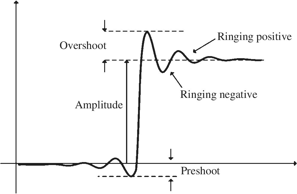
Figure 2.2 An illustration of preshoot, undershoot, and pulse ringing.
In detector pulse processing applications, it is common to group pulses into fast and slow pulses. A fast pulse generally refers to a pulse with risetimes of a few nanoseconds or less. An example of fast pulses is a detector’s current pulses that normally have risetimes less than a few nanoseconds, but their durations may extend to a few microseconds. Fast pulses are normally used for timing and high counting rate measurements. Slow pulses, which are sometimes called tail pulses, have longer risetimes than fast pulses and are generally used for energy measurements. The term shaped pulse is usually used for detector tail pulses whose shape has been modified with a pulse processing circuit. The fast and slow pulses are called linear pulses. A linear pulse is defined as a signal pulse that carries information through its amplitude or by its shape. It is obvious that the amplitude of linear pulses may vary over a wide range and a sequence of linear pulses may differ widely in shape. Linear pulses that are either positive or negative are called unipolar. Pulses that have both positive and negative parts are called bipolar. In analog domain, the information in a detector output pulse can be carried by another type of pulses that are called logic pulses. A logic pulse is a signal pulse of standard size and shape that carries information only by its presence and absence or by precise time of its appearance. They are used to count events, to provide timing information, and to control the function of other instruments in a system. Pulses produced in all radiation detectors are initially linear pulses, and logic pulses are produced by a circuit that analyzes linear pulses for certain conditions, for example, a certain minimum amplitude. Although a logic pulse carries less information than a linear pulse, from technical point of view, logic pulses are more reliable since the exact amplitude or form of the signal need not to be perfectly preserved. In fact, distortions or different sources of noise, which are always present in any circuit, can easily affect the information in a linear pulse but would have much less effect on the determination of the state of a logic pulse. In some situations, the limited information‐carrying ability of the logic signal may be also overcome by combining several logic pulses. Typical waveforms of unipolar, bipolar, and logic pulses are shown in Figure 2.3.

Figure 2.3 An illustration of unipolar, bipolar, and logic pulses.
2.2 Operational Amplifiers and Feedback
Operational amplifiers, or op‐amps as they are more commonly called, are one of the basic building blocks of analog electronic circuits. Op‐amps have all the properties required for nearly ideal dc amplification and are therefore used extensively in signal conditioning or filtering or to perform mathematical operations such as addition, subtraction, integration, and differentiation. The symbol for an op‐amp is shown in Figure 2.4. An op‐amp, in general, has a positive and a negative bias supply, an inverting and a non‐inverting input, and a single‐ended output. Practically speaking, an amplifier is regarded as op‐amp if it has a high voltage gain, typically 106–1012, its frequency response extends down to dc, and it is phase inverting. It is also required that it has a very high input impedance and a low output impedance. In the analysis of op‐amp circuits, it is assumed that the input voltage is very small because the input current to the amplifier is very small. This is equivalent to say that an op‐amp’s input is virtually at ground potential. This is known as virtual ground principle and forms a very convenient way of analyzing op‐amp circuits. One should note that the input terminal cannot be really at ground potential; otherwise there would be no amplifier output.

Figure 2.4 The operational amplifier.
Op‐amps are widely used with external feedback components such as resistors and capacitors between the output and input terminals. These feedback components determine the resulting function of the amplifier. A block diagram of an electronic amplifier with negative feedback is shown in Figure 2.5. In a feedback circuit, a portion of the output is fed back to the input. Then the voltage at the input is given by
where β is the feedback factor. The relation between the amplifier input and output is given by

Figure 2.5 A block diagram of an operational amplifier with feedback.
This gain is called the open‐loop gain and it applies whether feedback is present or not. The gain with feedback is called the closed‐loop gain and is related to the open‐loop gain with
So if the open‐loop gain is large enough, the closed‐loop gain of the system is given by
As an example, a basic summing amplifier using an op‐amp is shown in Figure 2.6. By applying the virtual ground principle to the circuit of Figure 2.6, one can write

Figure 2.6 A sum circuit using an operational amplifier.
The virtual ground principle also implies that the input current to the amplifier is zero; hence
By substituting for these currents from Eq. 2.6, one gets the relationship

If R = R1 = R2 = R3, then the output voltage is the sum of input voltages together with a sign inversion:
A special case of feedback on op‐amps is obtained by simply connecting the negative input and output of the op‐amp. This results in the voltage follower or unity gain buffer shown in Figure 2.7. This circuit essentially makes a copy of the input pulse at the output. It does that without drawing any current from the source of input voltage while at the output one can draw sufficient amount of current. This configuration is commonly used to effect isolation between stages of a pulse processing system by performing the connection while preventing interaction in the form of the second‐stage drawing current from the first stage. A use of such buffer circuits is discussed in Section 2.3.4.

Figure 2.7 Unity gain buffer or voltage follower.
2.3 Linear Signal Processing Systems
An analog pulse processing system is a device, or collection of well‐defined building blocks, which accepts an analog excitation signal such as a detector pulse and produces an analog response signal. A pulse processing system can be represented mathematically as an operator or transformation T on the input signal that transforms the signal into output signal. A symbolic representation of such system is shown in Figure 2.8. A simple example of a pulse processing system is a gain amplifier. A gain amplifier modifies the amplitude of the input signal by a gain factor at every time instant. The transformation of input signal x(t) to output signal y(t) in such amplifier can be written as
where a is a constant. A pulse processing system is linear if and only if it satisfies the superposition property, which is described as
where a and b are arbitrary constants. One can simply check that the gain amplifier described previously is a linear system. In principle, a linear circuit contains only linear components. Figure 2.9 shows the relation between the terminals of basic electrical components. From these relations, one can easily realize that any network of resistances, capacitances, and self‐inductances is a linear circuit. Op‐amps are also linear elements. However, not all commonly used circuits are linear, for example, a circuit with a diode is not linear. In practice, in all linear systems, the property of linearity applies over a limited range of inputs, and all systems cease to be linear if the input becomes large enough.

Figure 2.8 Signal processing system as an operator.

Figure 2.9 Basic relationships between terminal variables for electrical components.
Another useful property in the analysis of electrical systems is the concept of time invariance. Time invariance means that if y(t) is the response of the system to an excitation x(t), then the response of a delayed excitation x(t − τ) is y(t − τ) where τ is the amount of delay. In other words, if the input is delayed by τ, the response is also delayed by the same value. Linear time‐invariant (LTI) systems exhibit both the linearity and time invariance properties described previously. LTI systems are of fundamental importance in practical analysis because they are relatively simple to analyze and they provide reasonable approximations to many real‐world systems. The front‐end electronics of radiation detectors, or at least their first stages, are typically linear and time‐invariant signal processing devices, and thus our focus is on LTI systems. An additional property of physical systems, which holds true if we are considering signals as a function of real time t, is that of casuality. A system is called casual if the outputs do not depend upon future values of input. This means that for a causal system, the output signal is zero as long as the input signal is zero. A system is also called stable if a bounded input signal produces a bounded output. Although in a practical system no signal can grow without limit, variables can reach magnitudes that can overload the system. Therefore, it is very important to make sure that a system is stable. The systems that are most likely to suffer instability are feedback systems because under certain conditions the feedback may change sign and reinforce the input.
As an example of the relation between the input and output of an LTI system, we consider a simple RC circuit as shown in Figure 2.10. One can easily write the following relations by using the Ohm and Kirchhoff’s law:

Figure 2.10 The input–output relation of a simple RC circuit.
By using the relation between the voltage and current of the capacitor, one obtains the relation between the input and output voltages of the RC circuit as
Equation 2.13 is a differential equation containing only the input and output variables. In general, such relation can be written for any casual LTI system, and the relation is called the differential equation. The differential equation plays a very important role in the analysis of LTI systems. The general form of this equation is written as [1, 2]
where x(t) and y(t) are, respectively, the input and output signals of the systems and the coefficients a and b are independent of time. If the input signal is known, solution of this equation will give the system response. Unfortunately, this solution is a tedious affair and is not suitable for deign purposes. A more practical approach for analyzing the response of a system to a complicated function can be achieved by using the response of the system to a simple basic function. This can be achieved in time domain or in the frequency domain. These approaches will be described in the following sections.
2.3.1 Time Domain Analysis
In the description of an LTI system in the time domain, understanding the concept of Dirac delta function is necessary. In mathematics, the Dirac delta function δ(t) is a generalized function, or distribution, on the real number line that is zero everywhere except at zero, with an integral of one over the entire real line. This means that δ(t − t˳) is a delta function concentrated at t = t˳. A general definition of delta function is given by
but with the requirement that
In plain engineering language, δ(t) can be described as an even, tall, and narrow spike of finite height with zero width concentrated at t = 0. We also use scaled and shifted delta functions that are shown in Figure 2.11.

Figure 2.11 Representation of the unit length, shifted and scaled delta functions.
An LTI analog system is characterized in the time domain by defining its impulse response. The impulse response is the output of the system when the input is the delta function δ(t) and is typically denoted by h(t). When a delta function voltage pulse like those shown in Figure 2.11 is applied at the input of a system, the output pulse is not a delta function but is a pulse with a finite width and usually amplified or attenuated. This happens for any input pulse, but it is possible to obtain the output for the arbitrary input if the impulse response is known. This is achieved by using the concept of convolution. The convolution of two functions x(t) and y(t), denoted by x(t)*y(t), is defined by
The previous equation indicates that convolution performs integration on the product of the first function and a shifted and reflected version of the second function. Convolution has commutative, associative, and distributive properties. These properties are important in predicting the behavior of various combinations of LTI systems. The commutative property is described as
The associative property is described as
and the distributive property is described as
The output of a linear system y(t) to an input signal x(t) can be calculated by convoluting the input signal with the impulse response of the system as
For casual systems, which are of our interest, y(t) = h(t) = 0 for t < 0. Therefore, Eq. 2.21 is rewritten as

This relation can be interpreted in this way that it provides a measure of how the inputs previous to time t affect the output at time t. In fact, the impulse response is a form of memory: it weights previous inputs to form the present output. By having the impulse response, one can fully analyze the system properties. A system property that can be obtained from the impulse response is that of system stability. It can be shown that the output of a system is bounded if the following condition is satisfied by its impulse response function:
If the impulse response meets this condition, it is said to be absolutely integrable. Although Eq. 2.23 can be used to test the stability of a system, this approach is difficult for complicated systems. As it is shown in the next section, stability analysis is more convenient in frequency domain and by using the Laplace transform.
Since it can often be practically difficult to generate an analog delta function pulse accurately, it is easier to determine the response of the system to the unit step function that can be produced rather accurately. A unit step function is shown in Figure 2.12. The unit step function can be described as


Figure 2.12 The unit step function.
The previous definition of the step function relates it to the impulse delta function with
The impulse function is the derivative of step function, which means that we can determine the impulse response function of an LTI system from its response to a step function by using the linearity property of the system. If ρ(t) is the response of the system to the unit step function, then the impulse response function is related to the unit step response according to
In the following, we use the concept of convolution to analyze the response of a simple RC circuit to a single rectangular pulse of width T˳ and amplitude V˳. The impulse response of a RC circuit is given by
where RC is called the time constant of the system. The input rectangular pulse can be described by using the step function as
By taking the convolution of the input signal and impulse response, the output is calculated as

Figure 2.13 shows the output pulse shape for various values of time constant compared with the pulse width. It is seen that for RC ≫ T˳, the output approximates to the integral of the input pulse. For this reason, this circuit is called an integrator circuit. For small values of RC compared with the input pulse width, the pulse is transmitted with negligible distortion. Similarly, one can obtain the output of a CR filter to a rectangular input pulse as shown in Figure 2.14. It is seen that for RC ≪ T˳, the output approximates the differential of the input pulse. For this reason this circuit is called differentiator. For large values of RC compared with the pulse width, the initial part of the pulse is transmitted with negligible distortion followed by a very long undershoot. As it will be discussed later, in radiation pulse processing, the pulse undershoot created by the CR circuit formed between the different stages of a pulse processing circuit can be problematic at high rates as it can affect the measurement of the amplitude of the next pulses.

Figure 2.13 The output of an RC integrator for a rectangular input pulse.

Figure 2.14 The output pulse of a CR differentiator for a rectangular input pulse.
2.3.2 Frequency Domain Analysis
Analysis in frequency domain is achieved with the help of suitable transformations that yield equivalent results to those that would be obtained if time domain methods were used. However, in many situations, frequency domain analysis is more convenient and can even reveal further characteristics of signals and systems. For example, stability analysis is easier to perform in the frequency domain. The most important transformations in frequency domain analysis are the Fourier transform and the Laplace transform. In the following, we summarize the principal relationships and examples of the analysis of pulse processing systems by using the Fourier and Laplace transforms that are required for later discussion of the actual detector and front‐end circuits. Further details of these techniques can be found in several textbooks [1, 2]. The Laplace transform of a time‐dependent function f(t) is defined by
where s is a complex number with real part σ and an imaginary part ω as s = σ + jω. This definition is called the bilateral Laplace transform because the integration extends from −∞ to ∞. In the case where f(t) = 0 for t < 0, the transform is equal to the unilateral Laplace transform, which has a lower integration limit of zero. Some properties of the Laplace transform are summarized in Table 2.1. The proofs of these relations can be found in Refs. [1, 2].
Table 2.1 Some basic properties of the Laplace transform [1, 2].
| Property | Operation |
| Addition |
|
| Differentiation |
|
| Multiplication |
|
| Integration |

|
| Scaling |
|
| Damping |
|
In the previous section, we showed that for an LTI system, the excitation and the response functions are related by an ordinary linear differential equation with constant coefficients (Eq. 2.14). If we assume a system is initially relaxed so that all initial conditions are zero, the Laplace transform of both sides of Eq. 2.14 combined with the differentiation property of the Laplace transform (see Table 2.1) leads to the algebraic relation between the Laplace transforms of the input X(s) = L[x(t)] and output Y(s) = L[y(t)] as

From Eq. 2.31, the transfer function of the system H(s) is defined as the ratio of the Laplace transform of the output signal to the Laplace transform of the input signal:

One should note that the input and output signals can be current or voltage signals. For example, preamplifiers are often described by the transfer function relating the input current to output voltage signal. The transfer function completely characterizes a system so that armed with the transfer function, the response of the system to a wide variety of inputs can be calculated. Recalling that the system output in the time domain is described as the convolution of the input and the impulse response of the system, one can realize that the convolution in time domain is transformed into multiplication in the Laplace domain with L[h(t)] = H(s). When working in the Laplace domain, one can use the concept of operational impedance Z(s) defined as

By using the relations between the voltage and current of the basic electric components shown in Figure 2.9, the corresponding operational impedances of the components can be obtained. The operational impedances are given in Figure 2.15. These relations turn the circuit relations to algebraic equations, and therefore, instead of having to solve a set of coupled differential equations in the time domain, we can solve a set of linear algebraic equations in the Laplace domain.

Figure 2.15 The operational impedance of resistors, capacitors, and inductors.
The transfer function of that described by Eq. 2.32 can be modified in the form of

where z1, z2, …, zm are called the zeros of the transfer function and p1, p2, …, pn are called the poles of the transfer function. The zeros and poles of a transfer function can be real or complex, but if they are complex, then they must occur in conjugate pairs. The transfer function of a linear signal processing device can be fully described by its poles, zeros, and the constant gain factor K. In particular, the stability of a system can be conveniently analyzed by the location of poles in the complex s‐plane, which is called pole–zero plot of the system. The stability analysis by using the pole–zero plot is illustrated in Figure 2.16. It can be shown that if the poles are in the left‐hand plane of the plot, then they represent a stable system. If the poles are in the right‐hand plane of the pole–zero plot, then they represent an unstable system. A system with poles on the axis is referred to have marginal stability. As an example of stability analysis, consider a system with a transfer function of the form
where α is a constant. This system is stable if α < 0. The transfer function of this system in time domain represents an impulse response function of the form h(t) = eαt, which is obviously unbounded if α > 0.

Figure 2.16 Illustration of system stability from the system poles’ locations in the pole–zero plot.
So far, we have discussed the analysis of a system in the frequency domain by using the Laplace transform. The analysis of a system in the frequency domain can be also performed by using the Fourier transform. The Fourier transform of a time domain signal f(t) is defined as
with ω = 2πf. One can easily see that the Fourier transform is a special case of the bilateral Laplace transform (Eq. 2.30) with σ = 0. The inverse Fourier transform is given by
The Laplace and Fourier transforms of some of the common types of pulses are given in Table 2.2. While Laplace transform has no direct physical interpretation, the Fourier transform expresses the signal as a superposition of sinusoidal waves of frequency f with amplitudes |F(jω)| and relative phases as arguments of F(jω). The Fourier transform reveals the frequency contents of an arbitrary signal, which is often referred to as the spectrum.
Table 2.2 The Fourier and Laplace transforms of some common pulses.
| Function | F(jω) | F(s) |
Exponential decay (e−at)
|
|
|
Unit step function |
|
|
Unit impulse
|
1 | 1 |
All the frequency components play a role in the shaping of the function f(t); thus in order for an electronic device to perfectly treat the information contained in this signal, the device must be capable of responding uniformly to an infinite range of frequencies. Although in any real circuit there are always resistive and reactive components that filter out some frequencies more than others, it is practically only necessary to preserve parts of the signal that carry information. For nuclear pulses, these parts are amplitude and more particular the fast rising edge that normally cover the frequency range of 100 kHz to 1 GHz. The high‐frequency components allow the signal to rise sharply, while other frequencies account for the slow parts. Figure 2.17 shows the frequency components of two rectangular pulses of 100 ns and 1 µs durations, for example, detector current pulses. It is seen that while amplitude is a generally decreasing function of frequency, it never becomes identically zero, indicating that the rectangular pulse function contains frequency components at all frequencies. But, for pulses with shorter duration, the relative intensity of high‐frequency components is considerably larger.

Figure 2.17 Dependence of the frequency components of a rectangular pulse on its duration.
If the Fourier transform is applied to the system impulse response, one obtains the frequency response of the system. This function describes the ratio of the system output to the system input as a function of frequency. The frequency response of a system expresses how a sinusoidal signal of a given frequency on the system input is transferred through the system. If the input signals are regarded as consisting of a sum of frequency components, then each frequency component is a sinusoidal signal having a certain amplitude and a certain frequency. The frequency response expresses how each of these frequency components is transferred through the system. Some components may be amplified, others may be attenuated, and there will be some phase lag through the system. The similarity between the Laplace and the Fourier domain allows us to move easily from Laplace to the Fourier representation of a signal or system by setting s = jω. By setting s = jω into the transfer function of a system, we obtain the frequency response function H(jω) as

where the gain function is given by
The phase shift function is the angle or argument of H(jω):

Similar to the Laplace domain, the Fourier transform converts the time domain convolution to a simple multiplication. We have already introduced the concept of operational impedance in the Laplace domain. When working in the frequency domain, the concept of impedance is also very useful. Impedance is defined as the frequency domain ratio of the voltage to the current. If each electrical component is described by the differential equation relating voltage and current at its terminals, the corresponding frequency domain description is obtained by writing d/dt = jω. The ratio V(jω)/I(jω) then gives the impedance of the component. Impedance functions of some electrical components are given in Figure 2.18. The concept of impedance is very important in the analysis of a chain of pulse processing circuits. Amplifiers, and more generally any electronic circuit, have an input and output impedance. This means that if the input of the amplifier is part of some electronic circuit, it will behave as impedance Zin. Similarly, if the output of an amplifier is part of some electronic circuit, it will behave as an impedance Zout and a current or voltage source. A simplified representation of the input and output impedance of a typical circuit is shown in Figure 2.19. Both the input and output impedances in general involve capacitive or inductive components. The input impedance Zin represents the extent to which a device loads a given signal source. A high input impedance will draw a very little current from the source and therefore presents only a very little load. For most applications, input impedances of devices are kept high to avoid excessive loading, but other factors may sometimes dictate situations in which the input impedance must be low enough to load the source significantly. It is also generally desired for most applications that the output impedance to be as low as possible to minimize the signal loss when the output is loaded by a subsequent circuit.
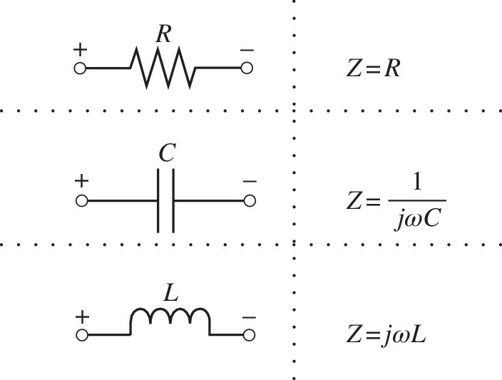
Figure 2.18 Impedance functions for resistors, capacitors, and inductors.

Figure 2.19 The input and output impedance of an amplifier.
2.3.3 Signal Filtration
Filtration of detector signals is a very important task in most nuclear pulse processing applications. A pulse filter, or just filter, is used to attenuate or ideally remove a certain frequency interval of frequency components from a pulse. These frequency components are typically noise though there are situations in which a filter is used to remove some part of the pulse as well. For example, the slow component of a detector pulse may be removed to avoid errors in timing measurement. A filter like any other system can be described in both the frequency and time domains, but it is more common to describe filters in the frequency domain. In the Laplace domain, a filter is described with its voltage transfer function. By replacing the variable s in the transfer function with jω, one can obtain the frequency response of the filter as well. The magnitude of the frequency response, sometimes called amplitude response or gain function, is given by

where Vi and Vo are the input and output voltages of the filter, respectively. The gain function is commonly expressed in decibels as
The phase response of the filter is also the argument of the frequency response. The filters are categorized based on the frequency bands that a filter attenuates or pass to low pass, high pass, band pass, and band stop. The gain function characteristics for ideal and practical filters of these types are shown in Figure 2.20. The passband is the frequency interval where the frequency components ideally pass through the filter unchanged. The stopband is the frequency interval where frequency components in this frequency interval are ideally stopped. The frequency range is divided into passband and stopband regions, and the frequencies that divide these regions are known as the cutoff frequencies. It can be shown that transfer functions for ideal filtering functions cannot be practically realized, neither with analog electronics nor with a filtering algorithm in a computer program. Due to this reason, the cutoff frequencies are practically assumed to be the frequencies where the gain has dropped by −3 dB, which is equal to 0.707 of its maximum voltage gain. Most systems have a contiguous range of frequencies over which the gain function remains approximately constant. This property gives rise to the concept of bandwidth that is defined as the interval of frequencies over which the gain does not vary by more than −3 dB. In some filter design applications, the filter requires to control the response as well as the gain response. This constraint will complicate the design of the filter and is not discussed here.

Figure 2.20 The gain function for ideal and practical filters.
Filters that only contain passive components such as capacitors, resistors, and inductors are referred to as passive filters. Active filters contain an element that gives power amplification. Modern active filters usually consist of passive elements connected in a feedback arrangement around an operational amplifier. The RC and CR filters shown in Figures 2.13 and 2.14 are simple passive filters with the following transfer functions:
The value τ = RC is the characteristic time constant of the filters. The gain and phase shift functions of these filters can be simply obtained by replacing s by jω and are given with

and


The gain functions of CR and RC filters are shown in Figure 2.21. At the frequency ω˳ = 1/τ, the input voltage is attenuated by 1/√2 ≈ 0.707 by both filters. Thus the −3 dB frequency is 1/τ. The CR filter attenuates frequencies ω < ω˳ while high frequencies are passing the circuit, so the CR filter is called a high‐pass filter. The RC circuit passes low frequencies, so an RC circuit is called a low‐pass filter.

Figure 2.21 The absolute value and phase of the transfer function of an RC and a CR filters.
In an amplifier system, the frequency response is normally limited at the upper end by capacitors inherent in the device used, which form low‐pass RC filters, and at the lower end by interstage coupling capacitors, which form high‐pass CR filters. The high‐frequency limitation affects the rapidly changing parts of the input signal. The degradation of the rapidly changing parts of the signal by a circuit, that is, the speed of the response of the circuit, may be characterized by the risetime (tr) of the circuit when the input is a step function. The risetime is an easily measured parameter and provides considerable insight into the potential pitfalls in performing a measurement or designing a circuit involving fast signals. The output of an RC filter to a step pulse of amplitude V˳ in the Laplace domain is obtained as
The inverse Laplace transform of Eq. 2.46 leads to the step response output as
The output of the RC filter increases exponentially from zero to V˳. The risetime tr of the step response as measured from 10 to 90% of the pulse leading edge is related to the to the upper −3 dB frequency by a useful relationship:
Recognizing that for a simple RC circuit −3 dB frequency equals (2πRC)−1, this is equivalent to
The RC and CR filters are first‐order systems. The order of a filter system is the highest power of the variable s in the transfer function. Higher‐order filters are obviously more expensive since they need more components and they are more complicated to design. However, higher‐order filters can more effectively discriminate between signal and noise. A second‐order transfer function that realizes a low‐pass filter is given by the following function:

where ω˳ is called the pole frequency and Q is the pole quality factor. The unit step responses of a second‐order low‐pass filter for different values of Q are shown in Figure 2.22. One can see that for high values of Q, the filter shows overshoot and the oscillations take long time to die out. Similarly, the transfer function of a second‐order high‐pass filter is given by


Figure 2.22 The unit step responses of a second‐order low‐pass filter for different values of Q.
2.3.4 Cascaded Circuits
Filters with transfer functions of increased order or complexity can be built by cascading two or more filters together. If the interstage loading between the successive stages is negligible, the overall transfer function of a filter cascade will be equal to a simple product of the transfer function of each of its individual stages:
where H1(s), H2(s), … are the individual transfer functions. To make the interstage loading negligible, the different stages should be isolated from each other. If two RC filters are not isolated as shown in Figure 2.23a, the combination of rules of the four impedances yields the transfer function:

Figure 2.23 (a) Series connection of two RC filters without isolation and (b) with isolation by a buffer amplifier.
This transfer function is obviously different from the product of two individual transfer functions of RC filters. The reason is that the second RC filter takes current out of the first filter so that the voltage at its output is different with when it is isolated. In order to eliminate the loading effect, we must introduce a voltage buffer, which was discussed in Section 2.2, between the stages. This is shown in Figure 2.23b. The buffer circuit produces an exact copy of the output of first RC filter to the second RC filter, thus eliminating the loading of the second stage to the first stage. In the previous section, we showed that the bandwidth of a first‐order low‐pass filter can be related to its risetime through Eq. 2.48. When several first‐order low‐pass filters are cascaded, the overall risetime can be approximated by
where trise1, trise2, etc. are the risetimes of the individual low‐pass filters. One very useful application of this equation is when using an oscilloscope. The risetime observed on the display will be a combination of the risetimes of the signals being measured and the cascaded transfer functions such as an amplifier chain or an amplifier under test, connecting cables, and oscilloscope itself. The step response of a typical low‐pass filter also will have nonzero delay in respect to the input signal. It is easy to show that from a cascade of several stages, the delay is the sum of the delays of each stage.
2.4 Noise and Interference
The output signals of radiation detectors are always subject to be contaminated with various sources of noise and interference signals. The effects of noise and interferences on the signals limit the accuracy of the information carried by the signal and may even disrupt a measurement. Noise and interference signals can be differentiated from each other based on the fact that the category of noise comes from within the apparatus itself and is inherently present in the system, while interference refers to distortions being applied to the circuit by another means, such as electromagnetic disturbances, ground loops, vibrations, power supply ripple, etc. Due to this reason interference signals are sometimes called external or man‐made noise. In radiation detection systems, noise is mainly generated in the detector and elements of the readout circuit attached to the detector such as resistors, diodes, field‐effect transistor, etc. The noise generated in the detector and readout system is added to the signal developed in the detector, and consequently, some amount of information in the signal is buried under noise as it is shown in Figure 2.24. One should note that the system response effects are part of an instrument’s response characteristics and are not considered to be noise or interference. While it is true that the noise produced by devices depends on their design and operation, some of the noise is a result of fundamental physical processes and quantities such as the discrete nature of electric charge and therefore cannot be avoided. However, the effect of noise can be reduced by using proper noise filtration strategies. The success of a noise filtration method depends on the proper characterization and model of the noise generating processes in the system. An accurate model of noise enables to design filters that effectively attenuate noise and pass the signal. On the other hand, interferences signals, at least conceptually, can be completely removed from the system. For example, an experimenter may eliminate the interferences by physically isolating the apparatus, applying electromagnetic shielding, or running the experiment at a different place. In the following sections, we review some basic noise concepts that are important in detector pulse processing, followed by a discussion of the common approaches for minimizing the interferences on detector signals. There are a number of good sources of information on electronic noise, and interferences that interested readers can consult for further details [3–7].

Figure 2.24 The effect of noise on a detector pulse amplitude.
2.4.1 Noise
2.4.1.1 General Definitions
The electronic noise generation is, in nature, a random process that appears as fluctuating currents or voltages. If we consider a random voltage signal e(t), the voltage signal would have a zero value when averaged for all time because it is randomly bouncing back and forth around the zero value. The average of the signal is not therefore a useful property for characterizing a noise signal. However, the mean‐square value of a noise signal is not zero. The mean‐square value is simply the average of the square of our voltage. The root‐mean‐square (rms) value of the noise signal is simply the square root of the mean‐square value and is commonly used for characterizing noise signals. The rms value of the signal is defined as

where T is the time period over which the rms value is measured. A noise signal, similar to any other random variable, can be also described by a probability density function. Some important sources of noise have Gaussian probability density functions, while some other forms of noise do not. Figure 2.25 shows graphically how the probability of the amplitude of a Gaussian noise relates to erms value. By definition, the variance of the distribution (σ2) is the average mean‐square variation about the average value, and the rms value is the standard deviation σ. In fact, physical scientists often use the term root mean square as a synonym for standard deviation. If σ is the standard deviation of the Gaussian distribution, then the instantaneous value of the voltage in 68% of the time lies between the average value of the signal and ±σ (or equally ±erms). Although the noise amplitude can theoretically have values approaching infinity, the probability falls off rapidly as amplitude increases so that 99.7% of the time the noise amplitude lies within a limit of ±3σ. Therefore, it is a common engineering practice to consider the peak‐to‐peak value of noise as 6σ or 6erms. The full width at half maximum (FWHM) of the noise distribution is also given by 2.36σ or 2.36erms.

Figure 2.25 Illustration of Gaussian noise parameters.
From elementary statistics we know that the variance of uncorrelated parameters is the sum of their variances. In an electric circuit different noise sources are caused by physically independent phenomena, and therefore, when there are multiple noise sources in a circuit, the rms value of total noise is given by the square root of the sum of the average mean‐square values of the individual sources:
where erms is the rms value of total noise voltage and ![]() ,
, ![]() , and
, and ![]() are the mean‐square voltages of the individual noise sources on their own. Similar considerations apply to current noise sources.
are the mean‐square voltages of the individual noise sources on their own. Similar considerations apply to current noise sources.
2.4.1.2 Power Spectral Density
If e(t) is a voltage signal, then its instantaneous power at any time t, denoted by p(t), is defined as the power dissipated in a 1 Ω resistor when a voltage of amplitude e(t) volts is applied to the resistor. The power is given by the multiplication of the voltage and the current, and for a 1 Ω load resistor can be expressed as
The average signal power is then given by

where T is a specified period of time over which the average is taken. This equation is equal to the mean‐square value of the signal. In fact, for a noise signal, which is of our interest, the numerical values of noise power and noise mean‐square value are equal; only the units differ. The concept of noise power is an essential tool for the characterization of electronic noise when it is expressed in the form of power spectral density G( f ). The power spectral density or power spectrum of a noise signal tells us how the average power (or the amplitude of the mean‐square value) is distributed over the frequency domain, and for this reason, it is called a density function. Figure 2.26 shows an example of noise signal and its corresponding power density. We can get the mean‐square value or variance of the noise signal for a specific frequency range by integrating G( f ) over the frequency range of interest as

Figure 2.26 (a) A noise signal in time domain. (b) The power spectral density of the noise signal.
Then, one can take the square root of the variance to get the rms value of noise.
Since noise spectral density is described as the power in narrow slices of frequency space, its unit is W/Hz. In most circuits, signals and noise are interpreted and measured as voltages and currents, and therefore noise power density is usually presented in two equivalent forms: V2/Hz or I2/Hz depending on the type of the noise (voltage or current). Figure 2.27 shows the noise voltage and current symbols. By having the noise power density, the rms values of the integrated noise voltage or current are given by

and

where ![]() and
and ![]() are the noise power densities for, respectively, voltage‐ and current‐type noises. We already discussed that for uncorrelated noises, the total variance of noise is given by the sum of the variances of individual noises. Since variance represents the noise power, this rule is also applied to noise power. When uncorrelated noises are present at the input of a network, the noise power at the output port of the network can be calculated by adding the noise power outputs arising from each source acting in isolation. Since the addition involves squared quantities, it is easy for some sources to dominate the output such that noise sources giving rise to small outputs can be ignored.
are the noise power densities for, respectively, voltage‐ and current‐type noises. We already discussed that for uncorrelated noises, the total variance of noise is given by the sum of the variances of individual noises. Since variance represents the noise power, this rule is also applied to noise power. When uncorrelated noises are present at the input of a network, the noise power at the output port of the network can be calculated by adding the noise power outputs arising from each source acting in isolation. Since the addition involves squared quantities, it is easy for some sources to dominate the output such that noise sources giving rise to small outputs can be ignored.

Figure 2.27 Representation of a noise voltage and a noise current source.
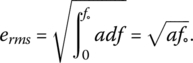
Depending on its power spectrum density, a noise process can be classified into white noise and colored noise. White noise theoretically contains all frequencies in equal power that produces a flat power spectrum over the whole frequency spectrum. Therefore, the total noise integrated over the whole spectrum is infinitive. But this is not practically important because any physical system has a limited bandwidth. For a band‐limited white voltage noise with a constant power spectrum up to a given frequency f˳, the power spectrum can be defined as
where a is a constant. We find the rms value of this noise as
The power spectrum of a colored noise has a non‐flat shape. Examples are pink, red, and blue noises. In general, one can assume a power spectral density of 1/f α where α determines the noise color. For white noise α = 0, while for pink noise α = 1 and red noise is represented with α = 2.
2.4.1.3 Parseval’s Theorem
In the previous sections, we asserted that the time domain representation f(t) and the frequency domain representation F(jω) are both complete descriptions of the function related through the Fourier transform. The energy of an aperiodic function in the time domain is defined as the integral of this hypothetical instantaneous power over all time:
Parseval’s theorem asserts the equivalence of the total energy in the time and frequency domains by the relationship
2.4.1.4 Autocorrelation Function
The correlation between two signals x1(t) and x2(t) is defined by the integral
When the two signals are different, it is common to refer to the correlation integral as the cross‐correlation function. If the two signals are the same, the integral is referred to as the autocorrelation function. The autocorrelation function of a random signal provides an indication of how strongly the signal values at two different time instants are related to one another. According to the Wiener–Khinchin theorem, the autocorrelation function of a random process is the Fourier transform of its power spectrum.
2.4.1.5 Signal‐to‐Noise Ratio
One of the common concepts used in noise measurement is signal‐to‐noise ratio (SNR). A signal contaminated with noise can be represented as x(t) = s(t) + e(t) where s(t) is the clean signal and e(t) is the noise signal. If s(t) and e(t) are independent of one another, which is usually the case, the mean‐square value of x(t) is the sum of the mean‐square values of s(t) and e(t):
Both the desired signal s(t) and the noise e(t) appear at the same point in a system and are measured across the same impedance. The SNR is defined as

which is equal to the ratio of signal power to noise power. It is common to express the SNR in decibels as

or
In charge measurement applications, the noise performance of the system is generally quantified with a parameter called equivalent noise charge (ENC), which is the amount of charge in the detector that produces an output pulse of amplitude equivalent to erms. In other words, the amount of charge that makes the SNR is equal to unity. This parameter will be further discussed in Chapter 4.
2.4.1.6 Filtered Noise
In previous sections we saw that when a signal passes through an LTI system or a filter, some frequency components of the input signal can be attenuated as governed by the filter transfer function. Figure 2.28 illustrates a noise signal at the input and output of an LTI system. In general, when a random signal enters a system, the output signal is also random, but its properties are altered from its original form. It is particularly important to know how the power spectral density is altered at the output. It can be shown that the relation between the power spectra of the input and output noise signals of an LTI system is given by [5]
where Gi( f ) and Go( f ) are, respectively, the input and output noise spectral densities and H(f) is the filter transfer function. If the input noise is described with noise voltage density (![]() ) or noise current density (
) or noise current density (![]() ), the rms values of output noise of an amplifier with a frequency response H( f ) are also calculated as
), the rms values of output noise of an amplifier with a frequency response H( f ) are also calculated as

and


Figure 2.28 Input and output noise signals of an LTI system.
In processing a detector pulse, one can improve the SNR by using filters that only pass the frequencies contained in the pulse and by removing the others. For example, if we send the band‐limited white noise described by Eq. 2.61 through an ideal low‐pass filter of unity gain with a sharp cutoff frequency f1 ( f1 < f˳), the output noise power spectrum will be given by

A comparison of this relation with Eq. 2.62 indicates that the noise rms value is reduced by a factor ( f1/f˳ )0.5, but if the frequency contents of the input pulse to the filter lie before the cutoff frequency, the rms value of the pulse remains unchanged, and therefore, the SNR improves.
2.4.1.7 Types of Noise
The various forms of noise can be classified into a number of categories based on the broad physical nature of the noise. This section covers the most important intrinsic noise sources for radiation detection systems: thermal (Johnson) noise, shot noise, flicker (1/f ) noise, and dielectric noise.
2.4.1.7.1 Thermal Noise
Thermal or Johnson noise is generated when thermal energy causes free electrons to move randomly in a resistive material. As a consequence of the random motion of charge carriers, a fluctuating voltage is developed across the terminals of the conductor. Thermal noise is intrinsic to all conductors and is present without any applied voltage. In 1927, J. B. Johnson found that such fluctuating voltage exists in all conductors and its magnitude is related to temperature. Later, H. Nyquist described the noise voltage spectral density mathematically by using thermodynamic reasoning in a resistor as [8]

where k is the Boltzmann constant and R is the resistor at absolute temperature T. Thermal noise is a white noise, and therefore the rms value of noise measured in bandwidth B is given by (4kTRB)0.5. Thermal noise is a universal function, independent of the composition of the resistor. For example, 1 MΩ carbon resistor and 1 MΩ tantalum resistor produce the same amount of thermal noise. One should note that an actual resistor may have more noise than thermal noise due to other sources of noise but never less than thermal noise. The thermal noise of a resistor may be modeled with an ideal noiseless resistor in series with a random voltage generator as shown in Figure 2.29a. The thermal noise can be also modeled with an equivalent Norton circuit including a random current generator in parallel with a noiseless resistor as shown in Figure 2.29b. The spectral voltage noise density is converted to a spectral current noise density as


Figure 2.29 Representation of thermal noise in a resistor with (a) a voltage noise source and (b) a current noise source.
Since thermal noise is a white noise, as the measurement bandwidth increases, the noise rms value increases, apparently without limit. In practice, the bandwidth of the circuit in which the noise is measured reduces at high frequencies, either as a result of deliberate bandwidth limiting or as a result of the stray capacitance of the resistor. The equivalent noise circuit of a resistor is shown in Figure 2.30. In this figure, the parasitic inductance of the resistor is ignored. The mean‐square voltage observed across the load resistor R is limited to an upper frequency set by C and R, which may be regarded as filter. The integrated rms voltage at the output is given by


Figure 2.30 Equivalent circuit of a real resistor with negligible parasitic inductance.
Somewhat surprisingly the magnitude of the thermal noise at the output depends on C and not R, but this is due to the bandwidth of the detector circuit. It should be mentioned that an ideal capacitor and inductors have no noise. But actual elements can have noise due to resistive components such as leakage resistance and the resistance representing dielectric loss.
2.4.1.7.2 Shot Noise
Shot noise is caused by the random fluctuation of a current about its average value and is due to the fact that electric current is carried by discrete charges. Shot noise was first noted in thermionic valves by Schottky. The shot noise is a white noise with a constant power spectrum density given by

where e is the electron charge and I is the mean current. Shot noise is important in semiconductor devices such as diodes and transistors, but the current passing through a resistor does not produce any shot noise. An important source of this noise in radiation detection systems is a detector’s leakage current.
2.4.1.7.3 Flicker Noise
This noise was first observed in vacuum tubes and was called flicker noise, but many other names are also used such as 1/f noise, excess noise, pink noise, and low‐frequency noise. It results from a variety of effects in electronic devices such as generation and recombination of charge carriers due to impurities in a conductive channel or fluctuations in the conductivity due to an imperfect contact between two materials [9]. This noise has timing characteristics, and therefore, it is frequency dependent. The frequency‐dependent noise power density is given by

where Af is a constant and is equal to the power spectral density at 1 Hz. The dependence of the power spectral density to inverse of frequency is the reason of calling this noise 1/f noise. 1/f noise plays an important role in the radiation detector systems. The input transistor of preamplifiers also generates 1/f noise. Some of this noise can be improved by manufacturing technology, while some 1/f noises can be hardly reduced.
2.4.1.7.4 Dielectric Noise
A capacitance without dielectric is noiseless, but practical capacitances have a dielectric medium between the plates. All real dielectric materials exhibit some loss and thermal fluctuations in dielectrics generate a noise. For dielectrics with relatively low conductance, the dissipation factor D is nearly constant and is given by
where G(ω) and C are the loss conductance and the capacitance of the dielectric at angular frequency ω. The noise power density due to dielectric losses is given according to Nyquist’s formula as

This relation shows that the noise power increases with frequency. This type of noise can be resulted from different elements of a circuit such as transistor packages as it has been discussed in Ref. [10]. Dielectric noise can be reduced by using dielectric materials with low losses such as quartz, ceramics, Teflon, and polystyrene.
2.4.1.8 Amplifier Noise
In an amplifier, every electrical component is a potential source of noise, and therefore, the noise analysis of an amplifier can be generally quite a complex task. To simplify the noise analysis of amplifiers, a noise model that represents the effect of all the noise sources inside an amplifier is generally used. In this noise model, the amplifier is considered as a noise‐free amplifier, and the internal sources of noise are represented by a pair of noise generators at the input. This noise model is shown in Figure 2.31 where a voltage noise generator (en) and a current noise generator (in) are placed at the input of the noiseless amplifier. We sometimes call en the series noise and in the parallel noise of the amplifier. A reason for the wide acceptance of this model is that the two noise sources can be measured with proper measurement strategies. It is possible to analyze the amplifier noise by considering that the two noise sources are significantly correlated or the noise sources have insignificant correlation. In the amplifiers of our interest, the noise sources are typically quite independent.

Figure 2.31 An amplifier noise model, where the noise is represented with a pair of noise sources at the input of a noiseless device.
2.4.1.9 Noise in Cascaded Circuits
An important task of amplifiers in nuclear pulse processing is to increase the amplitude of the pulses. This task is generally carried out in several steps. Therefore, it is important to know how the overall noise varies with the gain and noise of the individual steps. Consider an amplifier has two stages with gains A1 and A2 and with input noise rms values of e1 and e2. When a signal with rms value of sin is applied to the input of the amplifier, the relation between the signal and noise at the output can be written as

where sout and eout are, respectively, the signal and noise rms values at the output. This relation indicates that if the gain of the first stage is sufficiently high, the total noise performance is basically determined by the noise of the first stage. This is of practical importance because it implies that although the numerous elements of an amplifier can generate noise, it is only the noise from the first amplifying stage such as the first transistor and feedback that dominates the overall noise. The effect of a feedback resistor on the noise of an amplifier is discussed in the next section.
2.4.1.10 The Effect of Feedback
The application of feedback to an amplifier does not change the intrinsic noise of the amplifier, but it does affect the overall output noise of the amplifier by changing the gain of the amplifier and also the contribution of thermal noise from the resistive elements of the feedback [4, 7, 11]. An amplifier with resistor feedback is shown in Figure 2.32. To analyze the noise of this system, we first identify the noise sources present in the system. The signal source connected to the input has resistance Rs that produces the thermal noise es. The amplifier also has its input voltage and current noises en and in. The feedback resistor also produces thermal noise ef. As we are here interested only in the noise analysis, the signal source has not been shown. Now we find the output noise resulting from each source acting alone. The output noise (eo1) due to the amplifier input voltage noise en is calculated by the following relations:

Figure 2.32 The noise of an amplifier with resistor feedback.
The output noise due to feedback resistor noise ef is given by
The output voltage noise due to the amplifier current noise in is given by
The output noise resulted from the source voltage noise es is given by
By adding the noise spectral of the noise sources, and substituting the noise spectral densities of the resistors, the total noise voltage density at the output is given by

As it was calculated in the analysis of feedback applied to operational amplifiers, the gain of the amplifier is given by K = −Rf/Rs. By dividing the output voltage noise density by the square of the amplifier’s gain, the total equivalent input voltage noise density is obtained as

We can also find the equivalent input current noise by dividing the voltage noise by ![]() as
as

Thus, the thermal noise of the feedback resistor appears as a current noise at the input whose contribution is inversely proportional to the resistor value.
2.4.2 Interferences
We already mentioned that interference refers to the addition of unwanted signals to a useful signal and originates from equipment and circuits situated outside the investigated circuit. In general, interference results from the presence of three basic elements. These three elements are shown in Figure 2.33. First, there must be a source of interference. Second, there must be a receptor circuit that is susceptible to interferences. Third, there must be a coupling channel to transmit the unwanted signals from the source to the receiver. In radiation detection systems, the receptor mainly consists of the detector and its front‐end readout circuit where the signal level is small. The cables that transit detector pulses from location to location are also very vulnerable receptors of interferences. As an example, consider a detector system connected to the same ground potential as that of a high current machinery operating nearby. The interference signals may be produced by the machinery and flow into the front‐end circuit of the detector through the common ground that serves here as the coupling channel. From Figure 2.33, it is apparent that, in principle, there are three ways to eliminate or minimize interferences: (1) the source of interferences can be eliminated, (2) the detector and readout circuits can be made insensitive to the interference, or (3) the transmission through the coupling channel can be removed. Although it sounds that the best way to combat against the interferences is to eliminate their sources, these sources can never be completely eliminated in the real world. Thus, we always need to minimize the sensitivity of the measurement system to the interferences and/or eliminate the coupling channel between the source of interferences and the measurement system by a proper design of detector system and its associated electronics. A comprehensive discussion of interferences and methods of their elimination is beyond the scope of this book, and here we only briefly discuss some of the common sources of interference in radiation detection systems such as electromagnetic interferences (EMI), ground‐related interferences, and vibrations. Further details on various aspects of interferences can be found in Refs. [5, 12].

Figure 2.33 The elements of creating an interference problem, a source of interference, a receptor, and a coupling channel.
2.4.2.1 Electromagnetic Interferences and Shielding
EMI or “noise pickup” is an unwanted signal at the detector signals generated by electromagnetic waves. An EMI problem can arise from many different sources and can have a variety of characteristics dependent upon its source and the nature of the mechanism giving rise to the interference. There are also different ways in which EMI can be coupled from the source to the receiver [5, 13]. These ways include radiated, conducted, and inducted coupling. Radiated EMI is probably the most obvious and is normally experienced when the source and receiver are separated by a large distance. The source radiates a signal that can be captured by the detector and its front‐end part of the pulse processing circuit and added to the detector signal. Conducted emissions occur when there is a conduction route along which an unwanted signal can travel. For example, a wire that runs through a noisy environment can pick up noise and then conduct it to the detector circuit. Inductive coupling can be one of two forms, namely, capacitive coupling and magnetic induction. Capacitive coupling occurs when a changing voltage from the source capacitively transfers charge to the victim circuitry. Magnetic coupling exists when a varying magnetic field exists between the source and receiver circuit, thereby transferring the unwanted signal from source to victim. In radiation detection systems, sources of EMI can be due to the operation of equipment unrelated to the measurement system or resulted from the circuits and equipment related to the detector system such as power supplies, vacuum pumps, pressure gages, computers, etc. The prevention of EMI is an important design aspect in detector circuits, particularly in environments such as accelerators where various sources of interference may exist near the measurement system. The first necessary measure against EMI is to enclose the detector by a well‐designed Faraday shield, which is sometimes called Faraday cage. A Faraday cage isolates the inside circuits and detector from the outside world, thereby minimizing inductive interferences. A similar role is played by the shields of cables that isolate wires from the environment through which the cable runs. The effect of Faraday cage on the reduction of EMI depends upon various parameters such as the material used, its thickness, the size of the shielded volume, and the frequency of the fields of interest and the size, shape, and orientation of apertures in the shield to an incident electromagnetic field. However, for most applications a simple housing made out of a good conductor such as aluminum, copper, or stainless steel is sufficient to very effectively suppress the pickup noise. In addition to shielding against EMI, a Faraday cage may serve other purposes as well. In gaseous detectors such as proportional counters, the Faraday cage also serves as the cathode of the detector. In other types of gaseous detectors, the Faraday cage may be the enclosure of the operating gas. In semiconductor detectors, the detector housing, in addition to acting as the shielding against EMI, shields the detector against light because semiconductor detectors work as a photodiode and light can produce significant disturbance to the measurement. In nuclear physics experiments, the Faraday cage is the reaction chamber where detectors of different types are installed and normally operate in vacuum. The photomultiplier tubes (PMTs) working with scintillation detectors also require protection against EMI as well as against light. The PMTs are also sensitive to magnetic fields due to the deviations of photoelectrons and secondary electrons from their trajectories due to Lorentz force. Such protection is made by using magnetic shields such as mu‐metals. The protection of front‐end readout circuits can be made with a separate metallic shield, or they may be placed close to the detector inside the same Faraday cage. It is important to properly ground the shielding of the circuits because the parasitic capacitance that exists between the circuit and the shield can provide a feedback path from output to input and the preamplifier may oscillate. This problem can be avoided by connecting the shield to the preamplifier common terminal that eliminates the feedback path. The size of the susceptible circuit should be kept at minimum to reduce field‐coupled interference.
Although a Faraday cage minimizes the effects of EMI, there are always lines entering the Faraday cage, for example, power lines of the readout circuit, detector bias voltage, and input and output signal lines. Therefore, it is important to avoid noise from entering the cage with such lines. Figure 2.34 shows some of the basics of the design of a Faraday cage [14]. In general, no leads of any kind should enter a Faraday cage without their shield being properly connected to the detector enclosure at the penetration. Such connections are normally made by using suitable feedthrough connectors. The power supplies for the preamplifier should be well filtered, and it is useful, or sometimes necessary, to decouple the noise from the wires before they enter the circuit. The noise filters are usually connected to a ground plane of the electronic board, which itself is connected to the Faraday cage by a low‐impedance connection. The high voltage supply of the detectors should be connected to the Faraday cage by a proper RC filter to suppress the noise. Noise can also enter the Faraday cage through the signal output lines. In some applications, twisted pair cables are used to minimize the EMI from the output signal cables. An optical coupling between the front‐end readout and the acquisition system is also an effective way of minimizing interferences [15–17].

Figure 2.34 Faraday cage with input and output for signal and detector bias.
2.4.2.2 Ground‐Related Interferences
Grounding is one of the primary ways of minimizing interference signals and noise pickup. Grounds fall into two categories: safety grounds and signal grounds [5, 18]. Safety grounds are usually at earth potential and have the purpose of conducting current to ground for personnel safety. An ideal signal ground is an equipotential plane that serves as a reference point for a circuit or system and may or may not be at earth potential. In practice, a signal ground is used as a low‐impedance path for the current to return to the source. This definition implies that since current is flowing through some finite impedance, there will be a difference in potential between two physically separate points. Ground loops are formed by grounding the system at more than one point. Figure 2.35 shows a system grounded at two different points with a potential difference between the grounds. This can cause an unwanted noise voltage in the circuit. The effect of ground loops can be avoided by connecting the system to a single‐point ground. A common type of ground loop problem is faced when two components of a measuring system are plugged into two electrical outlets several meters apart. It is therefore a common practice to plug all equipment power lines into a common power strip that connects to the main electrical lines only at a single outlet. In some applications, ground loop can be avoided by the use of batteries to supply any necessary operating power units. There are also ground loops independent of the power line connections that can result from the interconnections between instruments. In such cases, the shield of the cables also serves to interconnect the chassis of each component with that of the next. If all chassis are not grounded internally to the same point, some dc current may need to flow in the shield to maintain the common‐ground potential. In many routine applications, this ground current is small enough to be of no practical concern, however, if the components are widely separated and internally grounded under widely different conditions, the shield current can be large and its fluctuations may induce significant noise in the cable [19].

Figure 2.35 Ground loop between two circuits.
The interferences resulted from ground loops are also closely related to EMI. A ground loop can effectively act as an antenna, and if electromagnetic radiation from external noise sources penetrates the setup, noise currents will be generated in the loop and added to the signal. Figure 2.36a shows how a ground loop can act as a coupling channel of EMI. The electromagnetic field penetrates the area between the ground plane and the signal cable. It therefore induces a current flowing through the circuit shielding, the ground plane, and the shield of the signal cable. A part of this current can be transformed into the measured signal. If it is not possible to disrupt the ground loop, the noise pickup can be reduced by reducing the area enclosed by the ground loop as shown in Figure 2.36b. It is also helpful to route the cable pair away from known regions of high magnetic field intensity.

Figure 2.36 (a) Ground loop acting as antenna and (b) minimizing the induction of signal in a ground loop by minimizing the enclosed area.
Another ground‐related interference resulted when the signal circuits of electronic equipment share the ground with other circuits or equipment. This mechanism is called common‐ground impedance coupling. Figure 2.37 illustrates the classic example of this type of coupling. In this case, the interference current, I, flowing through the common‐ground impedance, Z, will produce an interfering signal voltage, Vc, in the victim circuit. The interference current flowing in the common impedance may be either a current that is related to the normal operation of the source or an intermittent current that occurs due to abnormal events. In detector systems, it is necessary to isolate the ground of all the electrical devices such as pressure gages, temperature sensors, etc. from the Faraday cage with a suitable insulation fitting. A further action is to isolate the power line of the measurement system. The isolation can be performed in different ways among which the use of a proper isolating transformer is very effective in some radiation detection systems.
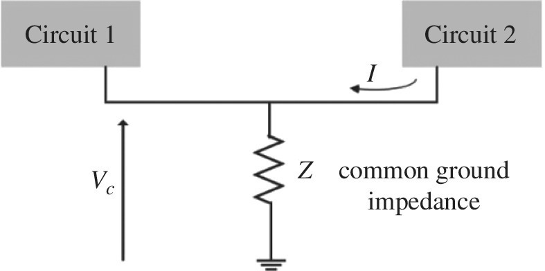
Figure 2.37 Interference due to a common ground.
2.4.2.3 Vibrations
Mechanical vibrations of a detector or preamplifier produce interference signals that are sometimes called microphonic noise. The production of microphonic noise is shown in Figure 2.38. Interference signals are caused by the mechanical movements of detector elements that change the capacitance of the detector. Because microphonic noises arise due to mechanical vibrations of the detector, they have some eigenfrequencies typical for the detector and/or the vibration source. Microphonic noise is particularly acute in gaseous detector with electrodes made of plastic foils due to their low damping factor. The most effective method of minimizing this noise is to remove the vibrations. However, if the vibrations cannot be perfectly removed, some degradation of detector performance will result when the frequency of the microphonic noises is near the frequency band of the detector signal. In such cases some noise filtration methods can be used to filter the interfering signals [20, 21].

Figure 2.38 Production of interference signals due to vibrations (microphonic noise) in a detector system.
2.5 Signal Transmission
2.5.1 Coaxial Cables
Pulses from radiation detectors can be strongly affected by the addition of interference signals to the pulses during their transport from location to location. In addition to the effect of interferences, the frequency contents of the pulses can be significantly attenuated during their transport. This is particularly important when transporting high‐frequency signals over the required distance that can be several meters. The degradation of the frequency contents of pulses stems from the fact that any configuration of conductors has stray capacitances, inductances, and resistance that will invariably attenuate some frequency components of the signal. To minimize the effect of interferences and degradation of the frequency contents of pulses, coaxial cables are used in many applications. In the following, we very briefly discuss the basic theory of pulse transmission, and more details can be found in Ref. [22]. The structure of a coaxial cable is schematically shown in Figure 2.39. It consists of two concentric cylindrical conductors separated by a dielectric material. The outer cylinder is generally made in the form of wire braid, and the dielectric material is usually made of materials such as polyethylene, Teflon, etc. The entire cable is protected by a plastic outer covering. The braided shield protects the inner conductor carrying the signal from any pickup noise and serves as the ground return. The coaxial construction also provides a well‐defined geometry for the connection so that one can know and control their electrical characteristics such as capacitance and inductance. The shielding action against low‐frequency electric fields is determined preliminary by the tightness of the braided shield, and high‐frequency electromagnetic fields are shielded by virtue of the skin effect. At the frequencies at which the skin depth is comparable to or smaller than the braid strand thickness, for example, above 100 kHz, the shielding is quite effective but will become less so at lower frequencies. In some applications it is necessary to surround the braid with a second shield or use doubly shielded coaxial cables to fully exclude the effects of very strong fields through which the cable must pass.

Figure 2.39 The structure of a coaxial cable.
For a coaxial cable consisting of two long concentric cylinders, separated by a dielectric, the capacitance and inductance per unit of length can be easily calculated as

where a and b are, respectively, the radius of the inner and outer cylinders and μ and ε are, respectively, the permeability and permittivity of the insulating dielectric. Typical values of L and C are on the order of 100 pF/m and a few tens of microhenry per metre. In real cables, there exists a certain resistance per unit of length (R) due to the fact that the conductors are not perfect. The insulation between the two conductors can be also imperfect, and thus the leakage current between them is described by a conductance per unit of length (G). Since the characteristics of a cable are distributed uniformly along the cable, we can model a small length of the cable by the circuit shown in Figure 2.40 [22]. If V(x) is the voltage between the two conductors at x, then by applying Kirchhoff’s law, the relation with voltage V(x + Δx) is given by
where I(x) is the current at x. If we let the length (Δx) become very small, this relation can be written as
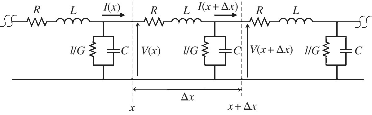
Figure 2.40 Schematic representation of a small portion of a transmission line [22].
Similarly, one obtains the relation of the current as
The combination of Eq. 2.90 and its derivative with respect to distance with the derivative of Eq. 2.91 with respect to time yields an equation that involves only V(x,t) as
In a similar manner, the equation of current is obtained as
To describe the fundamental features of a cable, we first assume a lossless cable, that is, R = G = 0. In fact, the attenuation in a cable is generally very small and only in long cables can be a problem. Then, the equations simplify to
These equations are the well‐known wave equation and indicate that pulse signals are transmitted through a coaxial line as a traveling wave. In other words, the electric and magnetic fields that comprise the electromagnetic pulse travel through the volume occupied by the dielectric. The solution of equations for a simple sinusoidal excitation such as V = V˳ejωt gives the traveling wave as
where k2 = ω2(LC) and V1 and V2 are constants to be determined by boundary conditions at the input and output ends of the line. Equation 2.96 represents two waves: one in x direction and the other in opposite direction −x. The wave propagating in −x direction is a reflected wave that becomes particularly important in timing measurements. The velocity of propagation is given by
The product LC is independent of length as long as the cable’s cross section is constant, and from Eq. 2.88 one gets LC = με, which indicates that velocity of propagation is only determined by the properties of the dielectric. The speed of signal propagation often is expressed as its inverse, the time of propagation per unit length (LC)−1/2. This quantity is known as the delay of the cable and is typically on the order of 5 ns/m for cables with 50 Ω characteristic impedance. The characteristic impedance is an important property of a transmission cable and is defined as the ratio of the voltage to current in the cable. An ideal lossless cable is given by

which is purely resistive. This is true if the only wave present in the transmission line is the wave traveling away from the measurement point. When the wave reaches the other end of the line, it may be reflected back, and the reflected wave will reach the measurement point, making the relation invalid. Therefore, only an infinitely long transmission line or a line terminated with its characteristic impedance will behave like a true resistor. The reflection of pulses from a cable not terminated with its characteristic impedance is discussed in the next section. The characteristic impedance depends on the dielectric material and diameter of inner conductor and outer shield of the cable but is independent of the cable length. Due to the dependence of Z˳ on the logarithm of the ratio of the radius of conductors, the coaxial cable impedances are limited to the range between 50 and 200 Ω. Some of the common coaxial cables are RG‐62/U (93‐Ω) for spectroscopy, RG‐58/U and RG‐174/U (50‐Ω) for fast timing and logic pulses, and RG59/U (75‐Ω) for high voltage transmissions. The response of a real cable to a simple sinusoidal excitation V(x) = Vejωt can be calculated from Eq. 2.92 as
where γ is a complex number known as propagation constant and is given by
Equation 2.100 can be recognized as well‐known wave equations whose general solution is
This is similar to a lossless cable but the term exp(±αx) represents the attenuation of the waves along the cable. It is easy to show that the general form of the solution for I(x,t) is similar for V(x,t) and also contains attenuated waves propagating in opposite directions. The velocity of propagation is given by v = ω/β. If frequency is high enough, the speed of propagation is approximately the same as an ideal cable and is given by v ≈ (LC)−1. The characteristic impedance of the line is given by

In this general relation, the impedance is complex, containing resistive and reactive components, but at high frequencies, it approaches to Eq. 2.97.
So far we have discussed the cable response to a sinusoidal excitation, while in nuclear applications we normally deal with pulses. A single pulse is composed of Fourier frequency spectrum with the amplitude of the spectrum decreasing for higher frequencies. If all these frequency components travel along the line at the same speed and experience no change, then it is obvious that they must arrive at the same time at the load and will add together to give the same waveform as at the input end. The phenomenon of pulse distortion arises when various frequency components arriving at the load have a different amplitude/or phase relation with respect to one another than they had at the input end. Thus, when they are added together, they must give different waveform. For long ideal cables, it was shown that sine waves propagate with no distortion, and thus a pulse arrives at the load with waveform identical to that at the input end but delayed in time by an amount equal to the length of the line divided by the velocity of propagation, that is, the delay time of the line. However, in a real cable, attenuation and propagation velocity depend on the frequency [22, 23]. Moreover, at high frequencies, the R and G vary [22, 23]. The variation of R with frequency is due to the skin effect that forces high‐frequency currents to flow through small cross‐sectional areas of the conductors, and variation of G is due to high‐frequency dielectric leakage. Therefore, some degradation of signals traveling a cable can happen. For slow pulses, however, the degradation of pulses is often insignificant, and the cable acts much like a simple conductor interconnecting components. The most significant parameter usually is the cable capacitance that increases linearly with cable length and is a critical problem when it connects the detector and preamplifier. For fast pulses, the cable characteristics are quite important and significant distortion of pulses may happen. The distortion of pulses is primarily due to the series resistance, but at frequencies above 100 MHz, the dielectric losses contribute more and more to the total losses, and at frequencies above 1 GHz, they may predominate. Because of these effects, the pulse response of a coaxial cable is strongly waveform dependent, and the response of a cable to a pulse of limited duration is strongly influenced by the width of the pulse. For practical purposes, it is often sufficient to know the risetime and attenuation of a cable for a step function input. The 0–50% risetime of the output is controlled by the high‐frequency response of the coaxial line, while the remaining 50–90% risetime may be approximately described by an RC time constant where R is the value of the termination resistance and C is the shunt capacity of the cable. The step pulse response of a cable with series resistance and dielectric losses is shown in Figure 2.41 [23, 24]. It is shown that the pulse after it has passed through a certain length of the cable does not anymore present a flat top and its amplitude is attenuated depending on the length of the cable.

Figure 2.41 Schematic representation of the response of a real cable to an input step pulse.
2.5.2 Pulse Reflections
The ratio of the voltage to current of a pulse traveling down a coaxial cable is determined by the characteristic impedance of the cable that depends on the geometry of the conductors and on the dielectric insulating medium between them. When the pulse reaches the end of the cable and is transferred to the input of the receiving circuit, if the input impedance is equal to the cable impedance, the voltage and current remain in the correct ratio to pass the associated energy completely to the load, and the unit is said to be matched to the cable. If the impedances are different, the ratio of voltage to current will be different in the load, and thus a fraction of energy enters to the load and the rest is reflected back to the source. In nuclear applications, the presence of reflections can have serious consequences by distorting the shape of pulses or producing spurious counts. The reflections can be calculated by considering the boundary conditions at the interface. When a cable of characteristic impedance Z˳ is terminated by an impedance Rl, the ratio of the voltage to current must be equal to the impedances in the cable and also in the termination. This means that in the cable, we have
where V˳ and I˳ are, respectively, the voltage and current of the original signal and Vr and Ir are, respectively, the voltage and current of the reflected signal. The negative sign of Ir is due to its opposite direction with I˳. At the interface, where both waveforms are present, we also have the condition
From these relations, the reflection coefficient ρ is defined as
The polarity and amplitude of the reflected signal are thus dependent on the relative values of the two impedances. If Rl is greater than the cable impedance, then reflection will have the same polarity, but if Rl is smaller than the cable impedance, the reflected pulse will have opposite polarity. In the limiting case of infinite load impedance, the reflected amplitude is equal to the incident amplitude. Figure 2.42 shows some example of reflected waveforms for a rectangular input voltage pulse and a one‐way cable delay of T˳ [22]. In these examples, the source internal impedance is assumed to be the same as cable impedance.

Figure 2.42 Some examples of pulse reflection scenarios.
In the previous cases we assumed input pulses of zero risetimes. In reality, all pulses have a finite measurable risetime. When the risetime approaches the delay time of the line, the reflections may produce further changes in the waveforms. This effect in an ideal cable is illustrated in Figure 2.43. We assume that a step pulse with a linear risetime (TR) is applied to an ideal cable that is terminated with a resistance of value less than its characteristic impedance. For different cable delays, the input waveform can be obtained from a geometrical construction of the applied and reflected voltages superimposed with the proper time sequence. When the risetime is smaller than twice of the cable delay, the risetime of the pulses remains unchanged (Figure 2.43a). For a risetime TR equal to just twice the delay of the cable, the reflected pulse reaches to the input when the input has reached to its maximum and a sharp peak is produced (Figure 2.43b). When the delay is less than the pulse risetime, the reflected pulse arrives at the input end before the applied voltage has reached its peak value. The reflected voltage attempts to decrease while the applied voltage attempts to increase the total voltage at the input terminal. The result is a waveform with three distinct slopes, as illustrated in Figure 2.43c.

Figure 2.43 The effect of reflection on the risetime of a pulse for different cable delays.
In a cable that has improper terminations at both the load end and source end, a single pulse applied to the line will give rise to multiple reflections traveling back and forth between the two ends of the cable until eventually reflections die out, leaving the final voltage Vf on the load. Due to multiple reflections, the load receives a series of decreasing amplitude steps, reaching the final voltage in one of two ways shown in Figure 2.44, depending on the circuit parameters. The final amplitude is independent of the cable characteristic impedance and is only determined by the termination at the source Rs and load Rl because Z˳ is only of significance while the reflections are propagating. Thus, if the cable delays are small compared with the time scales of the pulses, for example, slow pulses, then our concern is only to deliver the source voltage to the load (Vf ≈ Vs), which can be achieved by making Rs ≪ Rl. However, to preserve the shape of fast pulses, it is important to remove the reflections. Most of the time, this can be achieved by proper termination at the load, but in practice, sometimes in spite of a cable termination, reflections occur and the cable should be also properly terminated at the source.

Figure 2.44 Step functions applied to a cable mismatched on both ends.
2.5.3 Pulse Splitting
In many situations, one needs to process the same pulse in different ways, which requires producing multiple copies of a pulse. One can do this by connecting the signal source to multiple cables, where the central conductors are simply connected together. This method leads to a corresponding attenuation of the pulse amplitudes, and also reflections can occur when a fast pulses are involved. For example, if an input cable is connected to two output cables, which all are of characteristic impedance Z˳, then the characteristic impedances of the two output cables appear in parallel to each other. Thus an input signal sees at the splitting their combined impedance of Z˳/2, and hence part of the signal will be reflected back into the input cable even if the output cables are correctly terminated. To overcome these situations, three center conductors can be connected together through a star network of three termination resistors, each Z˳/3, as shown in Figure 2.45. It is easy to show that the impedance viewed from end of the input cable is Z˳, and thus reflections at the junctions are eliminated [25]. Reflections at the far ends of the output cables will of course be removed by correct terminations there. In general, if a pulse divided between n cables of impedance Rl, a simple calculation shows that the termination resistance R should be

Figure 2.45 (a) Elimination of reflections in splitting a pulse by two cables. (b) Equivalent circuit looking from the end of the first cable.
A simple splitting of pulses between cables results in an unavoidable attenuation of the amplitude of the pulses that may be undesirable in some applications. Active circuits can be used to produce several identical copies of an input signal in terms of shape and height. Such units are commercially available and are called fan‐out units. Figure 2.46 shows a simple active pulse splitting circuit with a PNP bipolar junction transistor operating as an emitter follower [26]. It accepts 50 Ω input pulses and gives a very low output impedance essential for driving analog signals to 50 Ω loads. There are also circuits that accept several input signals and deliver the algebraic sum at the output. Such units are called fan‐in, and one application of them is in adding the outputs of signals from a large scintillation detector that is viewed with several PMTs. Both fan‐in and fan‐outs are also used for logic signals.

Figure 2.46 Circuit diagram of a simple active splitter [26].
2.6 Logic Circuits
2.6.1 Types of Logic Pulses
Three classes of logic pulses are commonly used in nuclear applications: standard logic pulses, fast logic pulses, and gate logic pulses. Standard logic pulses convey the message yes (or 1) or no (or 0) and are used for general applications such as pulse counting. Fast logic pulses are used for coincidence measurements and are generally produced by time discriminators that mark the arrival time of analog pulses. The risetime of such pulses is very short usually of order of few nanoseconds. The width of these pulses can be varied and is not usually of primary importance except when the pulse width determines the maximum practical counting rate of the system. In working with fast logic pulses, the distortion of pulses during transit by cables is also very important as it can degrade the quality of timing information. The third class of logic pulses is gate pulses, which are widely used in nuclear pulse processing to gate pulses that are fed into a linear gate (see Chapter 4). These pulses will cause the gate to open or close for a period of time equal to the width of the gate pulse. This means that the width of logic gate pulses is variable, and, in fact, it is the most important parameter to be adjusted in using these pulses.
2.6.2 Basic Logic Operations
In some applications, it is required to select events that satisfy certain conditions that can be represented as Boolean logic operations. Logic pulses are used to perform Boolean operations by using units that are called logic gates. In general, a logic gate implements a Boolean function on one or more logical inputs that carry binary states 1 or 0 according to their voltage levels and produces a single logical output. The binary states 1 and 0 are generally called high and low states. There are different families of logic gates such as transistor–transistor logic (TTL), complementary metal–oxide–semiconductor (CMOS) logic, emitter‐coupled logic (ECL), nuclear instrument module (NIM), etc., which differ in some parameters such as construction technology, speed of operation, and power consumption. An instrument built based on each of these system standards delivers a pulse in a certain range of signal levels for logic 1 and logic 0, and also there is a certain range of signal levels for either logics according to which a logic pulse can be accepted by the instrument. Figure 2.47 shows the voltage specifications of a logic signal. The left‐hand scale shows the specification for the input, and the right‐hand shows the specifications for the output. For each state, a voltage range is chosen to give immunity to noise spikes. When it is required to connect logic modules of different standard systems, one should make sure about the compatibility of the input–output range of the modules. There are also requirements on the input and output currents of gates. The rising and trailing edge of digital pulses should be also fast enough as poor leading and trailing edge can adversely affect circuit operation.

Figure 2.47 An illustration of a typical logic pulse.
The response of logic gates is defined by truth tables. Figure 2.48 shows the truth table for some of the common gates together with their electronic symbols. For simplicity we have considered just two input signals A and B though gates with more inputs are possible. In an AND gate, only if logic pulses in a voltage range corresponding to high state arrive simultaneously at channels A and B, then a logic pulse of high state will be generated; otherwise the output will be in low state and thus this gate is sometimes called coincidence gate. The NOT gate gives an output logic pulse that is the inverse of the input signal, which means if the input signal is a high state, the output signal will be a low state and vice versa. Another useful gate is anticoincidence gate. The logic of a two‐input anticoincidence circuit should produce an output logic pulse only when a pulse is received at input A and none simultaneously at input B or when a signal is received at input B and none at input A. As seen in Figure 2.48, this function is almost achieved by the OR gate, but an OR gate does not exclude coincident input signals. The logic circuit required in order to identify only those signals in two channels that are not coincident in time is known as an exclusive OR gate (XOR). In addition to the gates shown in Figure 2.48, many other logic gates can be produced, but, in principle, only NOT and AND or NOT and OR are required to generate any logic function. A useful discussion on logic gates in nuclear applications can be found in Ref. [27].

Figure 2.48 Truth tables and electronic symbols of some common logic gates.
2.6.3 Flip‐Flops
Flip‐flops are one of the fundamental building blocks of digital electronic systems and are used for various applications such as data storage, data transfer, counting, and frequency division. The flip‐flop is a two‐input logic device that remains stable in either logic state until changed by an incoming pulse on the appropriate input. The simplest form of flip‐flop is the set–reset (SR) flip‐flop. Figure 2.49 shows the logic symbol and the truth table of this flip‐flop. The two input signals are defined as set (S) and reset (R), while the output signals are Q and its inverse ![]() . When a flip‐flop is set, it is usually considered as having a 1 stored in it. The flip‐flop can be set by putting a pulse or temporary level 1 on the set input while keeping the reset input at 0. The output can be reversed by putting a temporary 1 or pulse on the reset input while the set input remains at 0. This places the flip‐flop in the reset state, which produces a 0 on the Q output and a 1 on the
. When a flip‐flop is set, it is usually considered as having a 1 stored in it. The flip‐flop can be set by putting a pulse or temporary level 1 on the set input while keeping the reset input at 0. The output can be reversed by putting a temporary 1 or pulse on the reset input while the set input remains at 0. This places the flip‐flop in the reset state, which produces a 0 on the Q output and a 1 on the ![]() output. Having a 1 on both inputs at the same time should not occur in normal operation, and if it does occur, the result will depend on the construction of flip‐flop. The most economical method of providing an SR flip‐flop is to cross two NOR gates as shown in Figure 2.50. If any input is in 1 state, it produces a 0 out of its NOR gate. That 0 is transmitted to the second NOR gate. With both inputs at 1, the second gate will produce a 1 output that will hold the first gate in the 0 state even after the original 1 level has been removed from its input. Other common variants of flip‐flops include D (data or delay), T (toggle), and JK flip‐flops whose description can be found in Ref. [28].
output. Having a 1 on both inputs at the same time should not occur in normal operation, and if it does occur, the result will depend on the construction of flip‐flop. The most economical method of providing an SR flip‐flop is to cross two NOR gates as shown in Figure 2.50. If any input is in 1 state, it produces a 0 out of its NOR gate. That 0 is transmitted to the second NOR gate. With both inputs at 1, the second gate will produce a 1 output that will hold the first gate in the 0 state even after the original 1 level has been removed from its input. Other common variants of flip‐flops include D (data or delay), T (toggle), and JK flip‐flops whose description can be found in Ref. [28].

Figure 2.49 The logic symbol of a flip‐flop and an SR flip‐flop made from a pair of cross‐coupled NOR gates.

Figure 2.50 A crossed NOR flip‐flop.
A register circuit is a device that can receive a temporary level such as a pulse and hold that level until instructed to change it. Registers record the pattern of several input pulses and store this pattern in a buffer where it can be read by an external device such as computer. The simplest form of storage register is the SR flip‐flop that may be considered as a 1‐bit memory. Data are normally stored in groups of bits that represent numbers, codes, or other information. It is common to take several bits of data on parallel lines and store them simultaneously in a group of flip‐flops. Further details on data storage can be found in Ref. [28].
References
- 1 A. V. Oppenheim, A. S. Willsky, and S. H. Nawab, Signals and Systems, Second Edition, Prentice Hall, Upper Saddle River, NJ, 1997.
- 2 L. Balmer, Signals and Systems: An Introduction, Second Revised Edition, Pearson Education, Upper Saddle River, NJ, 1977.
- 3 A. Van Der Ziel, Noise in Measurements, John Wiley & Sons, Inc., New York, 1976.
- 4 M. J. Buckingham, Noise in Electronic Devices and Systems, Ellis Horwood Limited, Chichester, 1983.
- 5 H. W. Ott, Noise Reduction Techniques in Electronic Systems, Second Edition, John Wiley & Sons, Inc., New York, 1988.
- 6 C. D. Motchenbacher and F. C. Fitchen, Low‐Noise Electronic Design, John Wiley & Sons, Inc., New York, 1973.
- 7 P. J. Fish, Electronic Noise and Low Noise Design, Macmillan Press Ltd, London 1993.
- 8 H. Nyquist, Phys. Rev. 32 (1928) 110.
- 9 V. Radeka, IEEE Trans. Nucl. Sci. 16 (1969) 17–35.
- 10 V. Radeka, IEEE Trans. Nucl. Sci. 20 (1973) 182–189.
- 11 Texas Instruments, Noise analysis in operational amplifier circuits, Application Report SLVA043B, 2007.
- 12 H. Spieler, Radiation Detector Systems, Oxford University Press, Oxford, 2005.
- 13 Analog Devices, EMI, RFI, and shielding concepts, MT‐095 Tutorial, 2009.
- 14 V. Radeka, Shielding and grounding in large detectors, Proceedings of 4th Workshop on Electronics for LHC experiments, Rome, September 21–25, 1998.
- 15 S. Samek, Nucl. Instrum. Methods A 328 (1993) 199–201.
- 16 M. Malatesta, M. Perego, and G. Pessina, Nucl. Instrum. Methods A 444 (2000) 140–142.
- 17 O. Adriani, G. Ambrosi, G. Castellini, G. Landi, and G. Passaleva, Nucl. Instrum. Methods A 342 (1994) 181–185.
- 18 H. W. Ott, Ground—A path for current flow, IEEE Proceedings, 1979 IEEE International Symposium on Electromagnetic Compatibility, San Diego, CA, October, 1979.
- 19 W. K. Brookshier, Nucl. Instrum. Methods 70 (1969) 1–10.
- 20 G. F. Nowak, Nucl. Instrum. Methods A 255 (1987) 217–221.
- 21 S. Zimmermann, Nucl. Instrum. Methods A 729 (2013) 404–409.
- 22 R. E. Matick, Transmission Lines for Digital and Communication Networks, McGraw‐Hill, New York, London, 1969.
- 23 H. Riege, High frequency and pulse response of coaxial transmission cables, with conductor, dielectric and semiconductor losses, CERN Report 70‐4, CERN, Geneva, 1970.
- 24 G. Brianti, Distortion of fast pulses in coaxial cables, CERN Report 65‐10, CERN, Geneva, 1965.
- 25 W. R. Leo, Techniques for Nuclear and Particle Physics Experiments, Second Edition, Springer‐Verlag, Berlin, 1994.
- 26 A. Jhingan, et al., Nucl. Instrum. Methods A 585 (2008) 165–171.
- 27 International Atomic Energy Agency, Nuclear Electronics Laboratory Manual, Technical Document (International Atomic Energy Agency), 530, Second Edition, IAEA, Vienna, 1989.
- 28 J. D. Kershaw, Digital Electronics, Logic and Systems, Third Edition, PWS‐Kent, Boston, MA, 1988.