8
Photoluminescence Properties
Yasuhiro Yamada1 and Yoshihiko Kanemitsu2
1Chiba University, Graduate School of Science, Department of Physics, 1‐33 Yayoi‐cho, Inage, Chiba, 263‐0022, Japan
2Kyoto University, Institute for Chemical Research, Gokasho, Uji, Kyoto, 611‐0011, Japan
8.1 Introduction
Many studies have been devoted to understanding the high photon‐to‐electricity conversion efficiency of perovskite solar cells. Since the transiently photoexcited electrons and holes dominate the photoconversion process, photoluminescence (PL) spectroscopy is one of the most suitable methods for evaluating solar cell materials and devices [1–5]. In addition, the energy conversion efficiency in solar cells depends on the external PL quantum efficiency of the semiconductor material, as derived from detailed balance calculation proposed by Shockley and Queisser [6]. Thus, accurate evaluation of both the radiative and nonradiative recombination channels is required. Hybrid perovskites demonstrate efficient band‐to‐band PL, suggesting large radiative recombination. In addition, time‐resolved PL measurements have revealed the extremely long carrier lifetime of halide perovskites [7, 8]. The carrier lifetime recently reached >30 μs even in solution‐processed perovskite thin films [9]. Long carrier lifetime means small nonradiative recombination, inducing long carrier diffusion length and small carrier recombination loss, which are the great advantage of perovskite‐based devices [10, 11]. The low nonradiative recombination rate in hybrid perovskites has been discussed in terms of defect tolerance and is related to the unique band structure [12–14]. PL spectroscopy is also a powerful tool to investigate the working principles of solar cells. The charge transfer process of photoexcited carriers from the perovskite layer to the electron/hole transport layer in perovskite solar cells can be examined by employing time‐resolved PL [15–18]. This chapter describes the fundamental PL properties of hybrid perovskite materials and explains the physics behind high‐performance of perovskite solar cells. Examples of materials and device characterization by PL spectroscopy are then introduced.
8.2 Overview of Luminescent Properties
Luminescence is a phenomenon in which a substance absorbs energy and then emits light. Several types of luminescence are classified based on the excitation source, such as PL (photoexcitation), electroluminescence (EL) (electron‐beam excitation), cathodoluminescence (CL) (electric field), mechanoluminescence (mechanical deformation), and chemiluminescence (chemical reaction). Among them, PL has been used as the most convenient evaluation tool to clarify the nature of the excited state of luminescent materials due to the high spatial and temporal controllability of light. For instance, time‐resolved measurements are possible by using a pulsed laser as well as spatial‐resolved spectroscopy through using a microscope.
As the simplest case describing optical absorption and PL processes, let us consider a two‐level system, as shown in Figure 8.1a: optical excitation occurs from the ground state to the excited state because of light absorption, followed by optical transition with light emission (PL) from the excited state to the ground state. Here, the resonance energy of the optical absorption and PL is the same, ℏω0. However, even when there is no fluctuation in the energy of the two levels, the absorption and PL spectra have nonzero linewidth when the lifetime of the excited state is finite. It is known that the optical spectrum has the following Lorentz shape function.
Figure 8.1 Schematic illustration for excitation (optical absorption) and emission (PL) in (a) a two‐level system, (b) a four‐level system displaying PL Stokes shift, and (c) a semiconductor.
The shape function is a Fourier transform of the motion of an electric dipole with damped oscillation (X(t) = A exp (−γt/2) cos (ω0t)), where the spectral linewidth (γ) is the relaxation rate of the excited state and corresponds to the homogeneous linewidth.
Next, let us consider a case where the energies of optical absorption and PL are different (Figure 8.1b). The energy difference between light absorption and light emission is called the Stokes shift, which is often observed in organic materials because structural changes occur owing to photoexcitation.
In semiconductors, it is necessary to consider an energy band structure composed of closely spaced orbitals that are usually considered as a continuum. Consider the optical transition between the high‐energy conduction band and the low‐energy valence band separated by the band gap energy Eg, as shown in Figure 8.1c. When the excitation light energy exceeds Eg, electrons and holes are generated in conduction and valence bands, which rapidly fall to the conduction band bottom and valence band top by thermalization, typically within the timescale of picoseconds. The radiative recombination of electrons and holes leads to light emission (PL). Although optical absorption and PL are reverse processes, the optical absorption and PL spectra are largely different because of thermalization. At thermal equilibrium, the principle of detailed balance requires the following relation between emission and absorption spectra, which is known as van Roosbroeck–Shockley relation [19]:
where R(ν), P(ν), and ϱ(ν) are the emission rate per unit volume, photon absorption rate, and density of photons with frequency ν, respectively. We can convert the photon absorption rate into the optical absorption coefficient, α, by P(ν) = α c/nr, where c and nr are the speed of light and refractive index. Further, ϱ(ν) is given by the Planck distribution at temperature T. Then, we obtain the following relation,
where h and kB are Planck constant and Boltzmann constant, respectively. This equation shows that the PL efficiency is high in a strongly photo‐absorbing material and that the PL spectrum emphasizes low‐energy optical transition because of (exp (hν/kBT)−1) term, which is more dominant at low temperatures. Note that this equation applies to only intrinsic semiconductors (not to heavily doped semiconductors).
In actual semiconductors, recombination without light emission, so‐called nonradiative recombination, also occurs (see Figure 8.2). Nonradiative recombination usually involves midgap states induced by defects or impurities and consists of multiphonon emission processes in which bandgap energy is transferred to a number of phonons rather than emitted as light. Shockley–Read–Hall model is often used to describe the defect‐mediated nonradiative recombination processes [20]. Auger recombination, which involves three carriers (electron–electron–hole or electron–hole–hole) occurring under intense photoexcitation, is also a nonradiative process; electron–hole recombination energy is used to excite another carrier to the higher state [21]. The ratio of radiative and nonradiative recombination directly determines the PL quantum efficiency and also the photoconversion efficiency of solar cells.
Figure 8.2 Schematic illustration for (a) radiative and (b) nonradiative recombination processes via trap state, and (c) nonradiative Auger recombination involving two electrons and a hole.
8.3 Room‐Temperature PL Spectra of a Hybrid Perovskite Thin Film
This section describes the PL spectra of CH3NH3PbX3 [CH3NH3 = MA; X = I, Br, and Cl] at room temperature. Figure 8.3 shows the room‐temperature PL spectra of a CH3NH3PbI3 thin film [22]. The optical absorption spectrum is also plotted in Figure 8.3. The PL spectrum has a single peak at 1.60 eV, which coincides with the onset of optical absorption. Almost no PL Stokes shift suggests the band‐to‐band PL, which contrasts with organic semiconductors that typically show large Stokes shifts due to the structural changes in photoexcited states. The optical absorption spectrum shows an abrupt onset near the band gap energy (1.61 eV) with a small Urbach energy [23–25]. The absorption spectrum shape near the band edge is well explained by assuming small exciton binding energy (∼5 meV) and spectral broadening [26]. The van Roosbroeck–Shockley relation (Eq. 8.2) holds between the optical absorption and PL spectra, suggesting that the PL origin is also the band‐to‐band optical transition.

Figure 8.3 Room‐temperature PL and optical absorption spectra of a CH3NH3PbI3 thin film.
Source: Kanemitsu and Handa [22]. Copyright (2018) The Japan Society of Applied Physics.
One of the unique features of the PL spectral shape of a hybrid perovskite is its broad linewidth (∼100 meV for MAPbI3). In general, the origin of spectral broadening is categorized into homogeneous and inhomogeneous broadening. Inhomogeneous broadening appears when the emission energy has a fluctuation, while homogeneous broadening is natural (lifetime) broadening and appears even when all oscillations have the same eigenfrequency. When the linewidth is inhomogeneous, the PL spectral shape varies with changing excitation photon energy within the PL emission band. As shown in Figure 8.4, the PL spectral shape is broad and independent of the excitation photon energy, meaning that the spectral broadening is homogeneous [27].
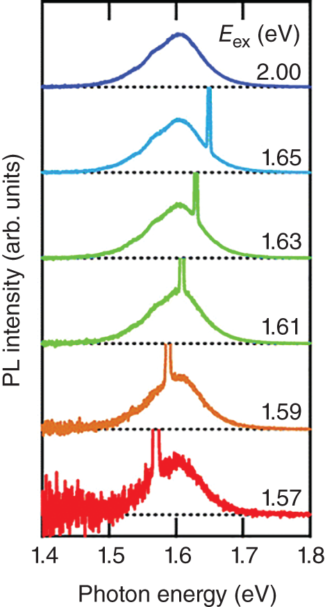
Figure 8.4 PL emission spectra of a MAPbI3 thin film under resonant excitation. The excitation energies are shown in the figure.
Source: Reproduced from Yamada et al. [27], with the permission of The Chemical Society of Japan.
Intriguingly, PL can be observed even when the excitation energy is slightly below the band gap energy. In this case, light emission above the excitation energy (anti‐Stokes PL) leads to semiconductor‐based emission cooling [28, 29]. The extremely strong anti‐Stokes PL occurring under low‐energy excitation conditions suggests a strong electron–phonon interaction in CH3NH3PbI3.
The PL emission energy of hybrid perovskites changes with halogen substitution, as shown in Figure 8.5a (PL peak energy MAPbI3: 1.6 eV; MAPbBr3: 2.3 eV; MAPbCl3: 3.2 eV). All these materials display strong room‐temperature PL, as shown in Figure 8.5b. The halogen substitution (I ➔ Br ➔ Cl) shifts the band gap energy to the higher energy side, which covers from the near‐UV to the near‐infrared spectral region [30]. While the room‐temperature PL mechanism is dominated by band‐to‐band recombination between free electrons and holes for MAPbI3 and MAPbBr3, exciton PL is observed for MAPbCl3 owing to the large exciton binding energy (∼40 meV) exceeding thermal energy at room temperature [31].
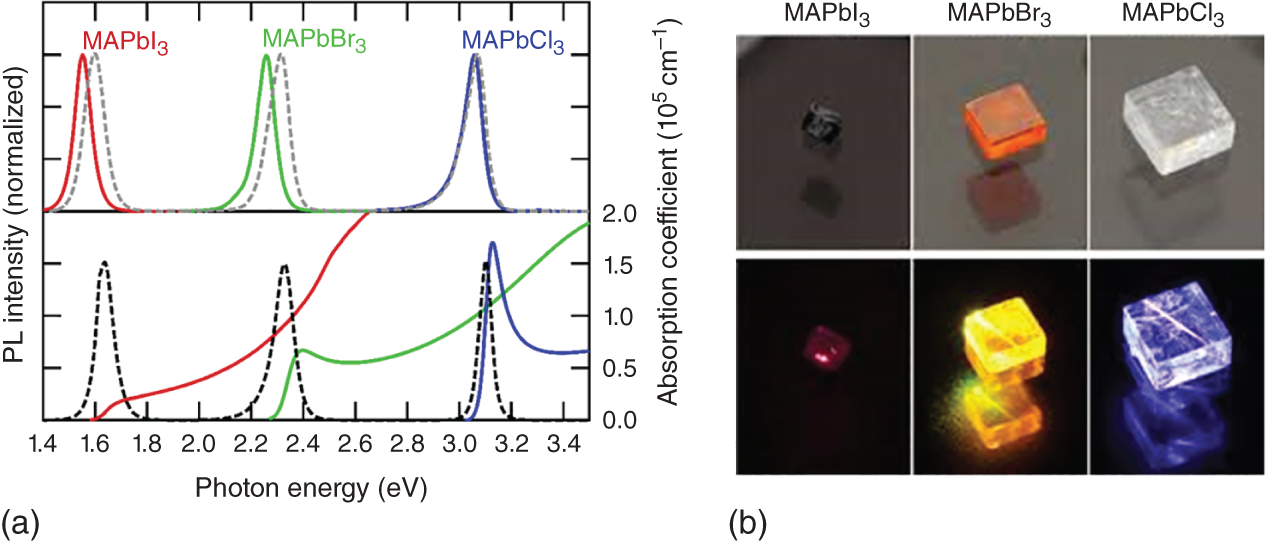
Figure 8.5 (a) PL spectra of MAPbI3, MAPbBr3, and MAPbCl3 thin films (dotted curves) and single crystals (solid curves). Optical absorption spectra are also plotted in the lower panel. The different PL spectral shape between thin films and single crystals is attributable to the photon reabsorption effect.
Source: Yamada et al. [30].
(b) Photographs of MAPbI3, MAPbBr3, and MAPbCl3 single crystals.
Source: Reproduced from Kanemitsu and Handa [22], with the permission of IOP publishing group.
Mixed halide perovskite MAPbX3 has also been fabricated and characterized [32–34]. Figure 8.6a shows the photographs of MAPbBr3−xClx and MAPbBr3−xIx nanocrystals colloidal solutions fabricated by anion exchange reaction [32]. The corresponding PL spectra are also displayed in Figure 8.6b. The PL energy can be changed continuously, covering all the visible range (400–850 nm corresponding to 1.5–3.1 eV). However, it should be noted that phase segregation occurs in mixed halide MAPbX3 due to ion migration under photoexcitation, which results in the appearance of new PL band at the higher energy [35–40]. As reported by E.T. Hoke et al., an additional PL peak forms at ∼1.68 eV for thin films of MAPb(BrxI1−x)3 and grows in intensity under continuous illumination (see Figure 8.7a) [35]. As schematically illustrated by Figure 8.7b, bromide and iodide ions are phase‐segregated upon illumination into higher‐bandgap Br‐rich and lower‐bandgap I‐rich domains.

Figure 8.6 (a) Schematic illustration for the reversible anion exchange reaction of MAPbX3 nanocrystals and photographs for MAPbBr3–xClx and MAPbBr3–xIx colloidal solutions. (b) Steady‐state photoluminescence spectra for the same films.
Source: Reprinted with permission from Ref. [32]. Copyright 2015, American Chemical Society.
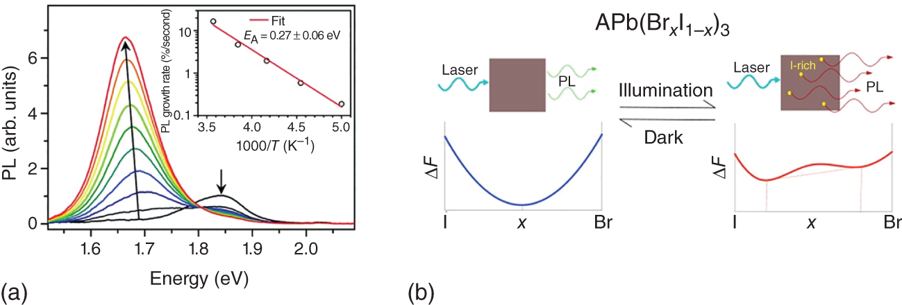
Figure 8.7 (a) PL spectra of a MAPb(Br0.4I0.6)3 thin film over 45 seconds in five seconds increments under above‐bandgap excitation at 300 K. The inset shows the temperature dependence of initial PL growth rate.
Source: Hoke et al. [35]. Licensed under CC BY‐3.0.
(b) Schematic of the proposed mechanism for photo‐induced phase segregation.
Source: Reprinted with permission from Ref. [36]. Copyright 2016, American Chemical Society.
The substitution of A‐site cation into CH(NH2)2 (= FA) and Cs also slightly changes the PL properties such as emission energy and linewidth; however, the PL mechanism itself is almost unchanged [41–44]. Pb2+ can also be replaced with Sn2+, and MASnI3 also shows band‐to‐band PL peaking at 1.25 eV, which shows redshift compared with MAPbI3 [45–48]. However, tin halide perovskites currently display poor PL efficiency compared with lead halide perovskites. The PL intensity from MASnI3 thin film is enhanced by the addition of SnF2 [49], which significantly reduces the unintentionally doped hole density (Figure 8.8).

Figure 8.8 PL spectra of the MASnI3 thin films prepared with SnF2 and without SnF2. The inset shows the PL spectra normalized at the peak intensity.
Source: Reprinted with permission from Ref. [49]. Copyright 2017, American Chemical Society.
8.4 Time‐Resolved PL of a Hybrid Perovskite
Since transiently photoexcited electrons and holes drive photoconversion processes, it is necessary to study the dynamical optical responses and reveal the optical properties of hybrid perovskites to improve the performance of perovskite‐based devices. Time‐resolved PL measurements provide information about electron–hole recombination processes in semiconductor materials. Here we discuss the carrier recombination processes of hybrid perovskites.
Figure 8.9 shows the time‐resolved PL spectrum (two‐dimensional contour image) of a solution‐processed CH3NH3PbI3 thin film obtained by a streak camera [50]. As shown in the inset, the PL spectrum shape is independent of time elapsed after pulsed laser excitation, and the PL peak appears at the onset energy of the optical absorption spectrum. The spectrum shape is independent of excitation laser fluence and photon energy.
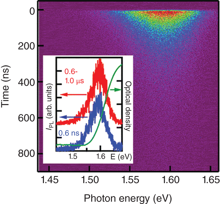
Figure 8.9 Two‐dimensional contour image of time‐resolved PL spectra of a MAPbI3 film. The inset shows the PL spectra at different delay times. The optical density spectrum is also plotted.
Source: Reprinted with permission from Ref. [50]. Copyright 2014, American Chemical Society.
Figure 8.10a shows the PL decay dynamics under different excitation fluence, where the PL intensities are normalized based on their maximum values [50]. Under weak excitation fluence, the PL dynamics show a slow and nearly monoexponential decay profile, while a fast and nonexponential component appears by intense photoexcitation. Figure 8.10b summarizes the effective PL lifetime and PL intensity immediately after the excitation as a function of excitation fluence. The effective PL lifetime t1/e is defined by IPL(t1/e) = IPL(0)/e, where IPL(t) represents the PL decay dynamics. The PL intensity immediately after the excitation shows a quadratic dependence on the excitation intensity at above 20 nJ/cm2, which evidences that bimolecular recombination dominates the recombination dynamics in this regime.
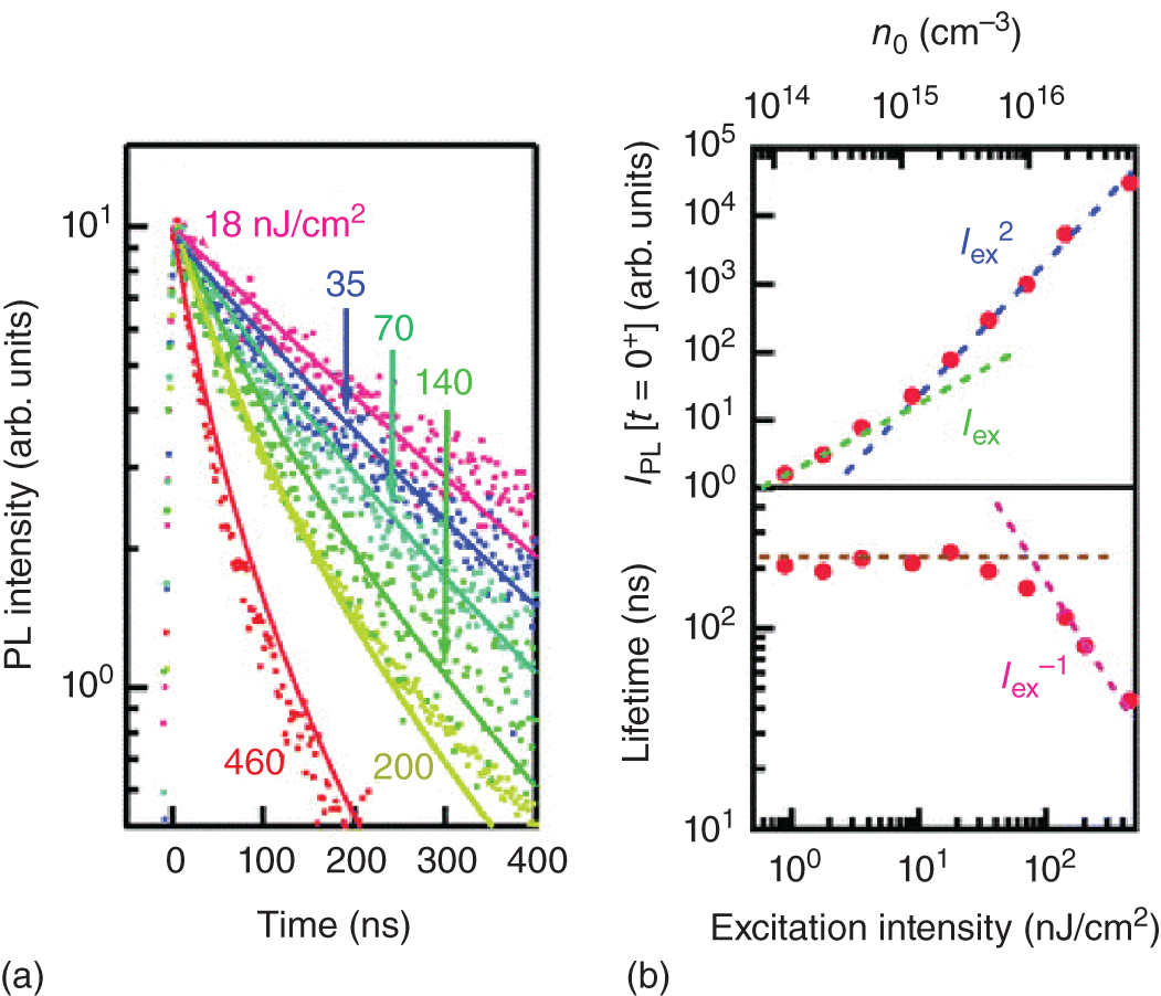
Figure 8.10 (a) PL dynamics of CH3NH3PbI3 thin film under different excitation fluence. (b) Excitation fluence (Iex) dependence of the PL intensity and effective PL lifetime. The initial photocarrier density n0 is shown along the top axis. The dotted lines are for eye guiding.
Source: Reprinted with permission from Ref. [50]. Copyright 2014, American Chemical Society.
At excitation intensities below 20 nJ/cm2, the PL intensity has a linear dependence on the excitation intensity. Thus, the recombination of photoexcited carriers and unintentionally doped carriers is responsible for the dominant light emission mechanism under weak excitation. The photocarrier density at the crossover point (∼1 × 1015 cm−3) corresponds to the carrier density resulting from unintentional doping. Considering that the perovskite thin film is fabricated by a solution process (i.e. simple spin coating method), unintentionally doped carrier density, which nearly equals the defect density, is surprisingly low, indicating a unique feature of hybrid perovskites called defect tolerance: defects/impurities are hardly incorporated or do not form deep states that promote the nonradiative recombination processes [51, 52].
The PL lifetime is inversely proportional to the excitation fluence under intense photoexcitation, while it remains nearly the same under weak excitation, indicating that the bimolecular recombination process is dominant under strong excitation. Such power‐dependent dynamics are well explained by a simple rate equation that includes single‐carrier trapping and two‐carrier (bimolecular) radiative recombination [50][53–55]:
Here n and p are the photoexcited electron and hole densities; An, Ap, and B represent the electron trapping rate, the hole trapping rate, and the bimolecular radiative recombination coefficient, respectively (see Figures 8.11a,b). Nn and Np are the electron and hole densities caused by unintentional doping. In the case that the photogenerated electron and hole densities are always the same (i.e. n = p, which strictly holds just after excitation), the aforementioned equations can be simplified to
where A = (An + Ap)/2 and N = Nn + Np. When the photocarrier density (n) is well above the unintentional doping (N), the effective PL lifetime can be approximately written as t1/e = 1/(A + Bn0), where n0 is the photocarrier density immediately after the excitation. This expression reproduces well the experimental results shown in Figure 8.10b.
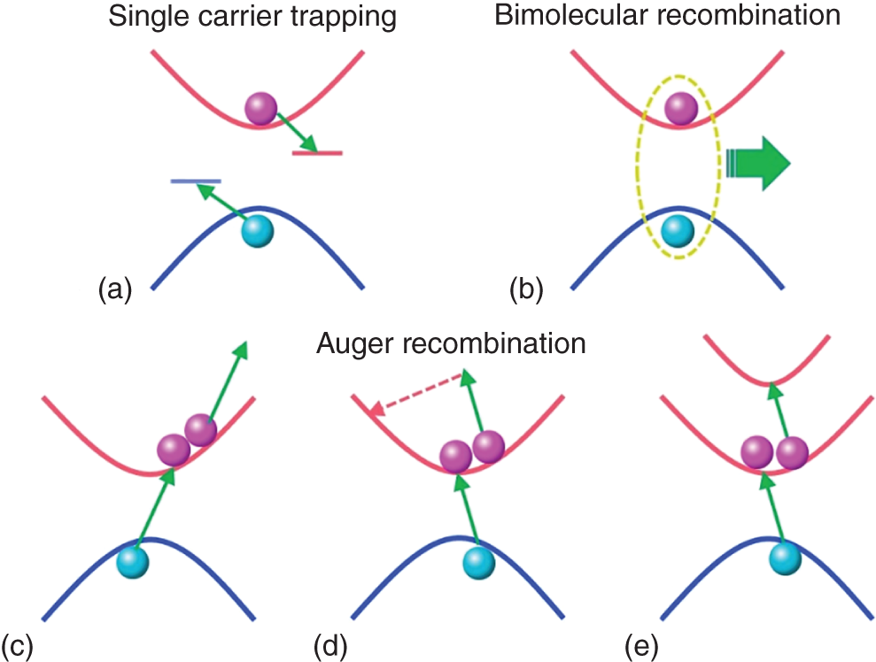
Figure 8.11 Schematic illustration of (a) single‐carrier trapping, (b) bimolecular recombination, (c)–(e) three types of Auger recombination involving three‐body (electron–electron–hole) processes: (c) direct Auger recombination; (d) indirect Auger recombination involving carrier‐phonon interaction ; (e) interband Auger recombination, where an extra electron is excited to second higher‐lying band.
The fact that the aforementioned equations well reproduce the PL dynamics is the evidence that free carriers, not excitons, dominate optical processes in hybrid perovskites because if excitons were dominant, IPL would not increase in proportion to the square of excitation fluence. The free carrier nature of MAPbI3 is consistent with its small exciton binding energy (Eb) compared with room‐temperature thermal energy (kBT = 26 meV at 300 K) [23, 26].
From the global fitting of the PL dynamics, we obtain A = 1.8 × 10⁷ s–1 and B = 1.7 × 10⁻¹⁰ cm3/s for this thin film. Note that A is sensitive to the density of defects or impurities, and thus it differs from sample to sample. On the other hand, B is an intrinsic material parameter, meaning that it is nominally independent of the sample quality. The radiative recombination coefficient B for MAPbI3 is comparable to that in typical direct‐gap semiconductors (e.g. GaAs: B ≈ 7.2 × 10⁻¹⁰ cm3/s). Such a high B coefficient is caused by the direct allowed interband optical transition. Generally, the radiative recombination coefficient (B) can be derived from the absorption coefficient, since the optical absorption and radiative recombination are reverse processes (c.f. van Roosbroeck–Shockley relation). The strong optical absorption coefficient also is consistent with the large B coefficient of hybrid perovskite.
Under much stronger excitation fluence, Auger recombination, that is, a three‐body nonradiative recombination involving electron–electron–hole or electron–hole–hole processes appears [21]. In Auger recombination, excess energy generated by the recombination of electrons and hole is used for the high‐energy excitation of the extra electron (hole). The high‐energy electrons (holes) rapidly fall to the bottom (top) of the conduction (valence) band accompanying phonon emission. When we consider the Auger process, Cnn2p and Cpnp2 terms should be added into Eqs. (8.4a) and (8.4b), where Cn and Cp are Auger coefficient for electron–electron–hole and electron–hole–hole processes, respectively. If n = p holds for any time, the rate equation is simply expressed as
These carrier recombination processes are schematically illustrated in Figure 8.11.
Similar PL dynamics have been reported in other hybrid perovskites such as MAPbBr3. However, the PL dynamics of MAPbCl3 should be different when excitons are dominant (i.e. the exciton binding energy is much larger than the thermal energy at room temperature) [31]. Table 8.1 shows the reported B and C coefficients for MAPbX3.
Table 8.1 Reported B and C coefficients of MAPbX3 measured by PL, pump‐probe transient absorption technique (TA), time‐resolved microwave spectroscopy (TRMC), and time‐resolved THz spectroscopy (THz).
| X | B (cm3/s) | C (cm6/s) | Methods | References |
|---|---|---|---|---|
| I | 1.7 × 10⁻¹⁰ | — | PL and TA | [50] |
| 23 × 10−10 | — | TA | [56] | |
| 0.98 × 10⁻¹⁰ | 0.68 × 10⁻²⁸ | TA | [57] | |
| 1.5 × 10⁻¹⁰ | 3.4 × 10⁻²⁸ | TA | [55] | |
| 13 × 10−10 | — | TRMC | [58] | |
| 9.2 × 10⁻¹⁰ | 1.3 × 10⁻²⁸ | THz | [59] | |
| 0.61 × 10⁻¹⁰ | 1.6 × 10⁻²⁸ | THz | [60] | |
| I1−xClx | 0.87 × 10⁻¹⁰ | 0.99 × 10⁻²⁸ | THz | [59] |
| Br | 4.9 × 10⁻¹⁰ | 13.5 × 10⁻²⁸ | TA | [55] |
Next, we focus on the PL dynamics under weak photoexcitation. When the excitation light fluence is small enough so that electron–hole radiative recombination and Auger recombination are negligible, PL lifetime corresponds to the inverse of nonradiative single‐carrier trapping rate, A. Because A is determined by the density of deep‐level defects and impurities, the PL lifetime under weak excitation can be a good metric for the sample quality.
In the early days of perovskite solar cells, the PL lifetime was as short as ∼8 ns [14]. However, it has been rapidly increased as the defect or impurity density of samples was reduced by improving fabrication methods [7–9, 15, 16, 50, 61]; thus, the efficiency of perovskite solar cells improved as well. Currently, the carrier lifetime longer than 30 μs has been reported by time‐resolved microwave conductivity [9], suggesting extremely small deep defect or impurity density.
Moreover, such long PL lifetime is quite surprising if we consider that solution‐processed CH3NH3PbI3 thin films form multigrain structure [4, 62–65]. In many semiconductors, the surface recombination rate is significantly larger compared with that in the bulk region. Thus, the grain structure should shorten the PL lifetime because of the large surface‐to‐volume ratio. In hybrid perovskites, a small surface recombination rate has been reported [66, 67], leading to the high device performance of perovskite thin‐film solar cells.
Related to the long PL lifetime, hybrid perovskite shows different PL spectrum and dynamics in thin films and thick single crystals owing to strong reabsorption of emitted photons (Figure 8.5a) [30, 68–74]. Because of the efficient PL, strong band‐to‐band emission, small Urbach tail, and long carrier lifetime, high‐energy PL is strongly absorbed, which results in the PL red shift for thick single crystals compared with the PL spectrum in thin films. Evaluation of the photon reabsorption effect is important to understand fundamental optical responses for optimal device design. This topic is discussed in the preceding Chapter 9.
8.5 PL Quantum Efficiency
Another indicator of sample quality is PL quantum efficiency. We often consider two types of quantum efficiencies. External quantum efficiency (EQE: ηext) is the ratio of the number of photons emitted outside of the material to the number of photons absorbed to the material (incident photons), whereas internal quantum efficiency (IQE: ηint) is the probability that a photogenerated electron and hole recombine radiatively.
EQE can be experimentally obtained by measuring emission intensity and reflectance with high accuracy. The integrating sphere is usually used to collect photons emitted in all directions (Figure 8.12a). The EQE value of a solar cell is directly related to its open‐circuit voltage, VOC [76, 77].
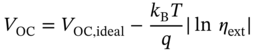
Here kB is the Boltzmann constant, T is the cell temperature, and q is the elementary charge. Voc,ideal accounts for the effect of incomplete absorption, thermalization, and solid angle of the solar illumination.
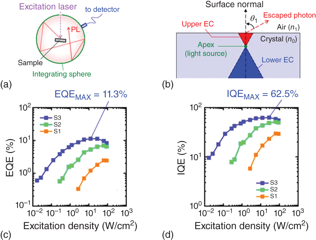
Figure 8.12 (a) Typical experimental setup for measuring PLQE. (b) Schematic illustration of escaping cone. (c), (d) EQE and IQE of PL for MAPbBr3 single crystals fabricated under different growth conditions as a function of excitation fluence. S1, S2, and S3 represent the crystals grown with the MABr concentration of 0.80, 1.00, and 1.25 mol/l, respectively.
Source: Reproduced from Ref. [75]. Copyright 2019, AIP Publishing.
The aforementioned equation can be derived as follows. First, let us consider a solar cell with an external PL efficiency of 100% and ideal open‐circuit under quasi‐equilibrium condition. At this time, the solar excitation rate and the external light emission rate should be balanced. When the external PL efficiency is ηext (≠1), the quasi‐equilibrium condition requires
where Rext is the external PL rate from the solar cell, and Psolar is the solar excitation rate. Assuming the PL rate is determined by the bimolecular recombination of electrons and holes, Rext should depend on the product of electron and hole densities, np, that is,

By combining this equation with Eq. 8.8, we obtain Eq. 8.7.
The aforementioned equation means that a semiconductor having a high PL efficiency is promising as a solar cell. High PL efficiencies of hybrid perovskites in thin films, quantum dots, and crystalline forms have been reported [70–72, 78–82] and are essential for the high performance of perovskite solar cells.
While we can experimentally evaluate EQE, IQE is more appropriate to discuss the optical processes and physics of light emission. For fluorescence particles and chemical molecules, the EQE value is usually close to the value of IQE owing to the large Stokes shift between absorption and emission energies. However, for solid‐state light emitters (especially direct band gap semiconductors), EQE is a complicated function of both IQE and light extraction efficiency, because PL photons are partially reabsorbed by the material. As schematically shown in Figure 8.12b, only the PL photons inside the escaping cone can be emitted from the crystal because of the total reflection. Because of these effects, the relation ηint ≫ ηext is usually satisfied. The IQE value is determined by a balance between the radiative and nonradiative recombination rates and thus is written by

where τrad and τnonrad are the radiative and nonradiative recombination lifetimes, respectively.
Figures 8.12c,d show the EQE and IQE values of a MAPbBr3 single crystal as a function of excitation intensity measured by omnidirectional PL spectroscopy [75]. Although the PL efficiency changes by fabrication conditions, it increases with excitation intensity under weak excitation. Several crystals were fabricated with different molar ratio of MABr and PbBr2 in the solution for crystal growth. Samples S1, S2, and S3 represent the crystals grown with the MABr concentration of 0.80, 1.00, and 1.25 mol/l, respectively. Here PbBr2 concentration is fixed at 1.00 mol/l. For sample 3 in Figure 8.12d, the maximum IQE reaches 62.5%. The IQE elevation is attributable to the saturation of nonradiative recombination centers. However, in the case of bulk MAPbBr3 crystals, PL lifetime is shortened under strong excitation [69], suggesting that the acceleration of the radiative process mainly occurs in bulk MAPbBr3. Further increment of excitation intensity induces the depression of IQE. A slight PL blue shift was simultaneously observed under intense photoexcitation and can be explained by the band‐filling effect [75].
The recombination model quantitatively explains the excitation‐intensity dependence of IQE by Eq. 8.6. According to Eqs. (8.6) and (8.10), theoretical IQE (ηcalc) can be calculated as
where n0 is the carrier density at equilibrium under continuous‐wave excitation. According to this equation, IQE has a maximum at a certain value, which is consistent with the experimental result [75].
Note that the IQE is significantly enhanced by changing the MABr concentrations in the feed solution as shown in Figure 8.13d, indicating that nonradiative recombination centers correlating with the cation vacancies dominate the nonradiative recombination processes.
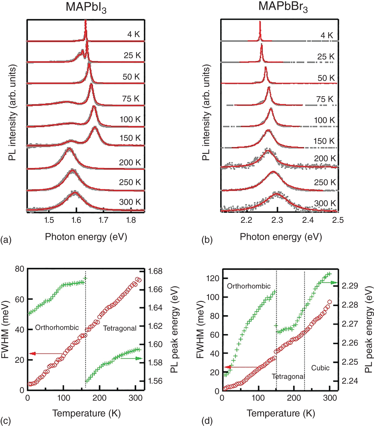
Figure 8.13 PL spectra of (a) MAPbI3 and (b) MAPbBr3 single crystals at various temperatures from 4 to 300 K obtained by PL microscopy. Solid curves represent the fitting results by pseudo‐Voigt functions. Temperature dependence of PL energy and linewidth of (c) MAPbI3 and (d) MAPbBr3. Dotted lines indicate the phase transition temperatures.
Source: Data Reproduced from [83].
8.6 Temperature‐Dependent PL
Temperature‐dependent PL properties (efficiency, emission energy, linewidth) provide vital information to understand the physical mechanism of the optical response in semiconductors. In many semiconductors, band gap energy (and also PL energy) monotonically decreases with temperature (Varshni's law). However, hybrid halide perovskites display drastically different behavior. One crucial feature is the phase transition. MAPbX3 perovskites undergo cubic‐to‐tetragonal and tetragonal‐to‐orthorhombic phase transitions with a decrease in temperature [84, 85]. Figure 8.13 shows the PL spectra of MAPbI3 and MAPbBr3 bulk single crystals measured at various temperatures [83]. The experiments were performed with an objective lens, and only the PL from the near‐surface region was collected to minimize the photon reabsorption effect. Lower panel ([c] and [d]) summarizes the temperature dependence of PL peak energy and linewidth. The PL peak positions shift with temperature because of the temperature dependence of the band gap energy. PL energy displays significant “jump” at the tetragonal‐to‐orthorhombic phase transition temperature. In contrast to the conventional semiconductors whose band gap energy obeys Varshni's law, the PL energy of hybrid perovskites increases with temperature owing to the unique band structure of lead halide perovskites: both conduction and valence bands consist of antibonding orbitals [86].
Unlike the case of PL energy, PL linewidth shows almost no change at the phase transition temperature. PL linewidth is determined by electron–phonon interaction and extrinsic inhomogeneous line broadening. A previous study suggests that the spectral broadening of the exciton is governed by the Fröhlich interaction rather than by charged impurity scattering [87]. The spectral width of the free exciton can be expressed as
where Γ0 is the temperature‐independent spectral width, ELO is the phonon energy, γLO and γac are the coupling strengths for LO phonons and acoustic phonons, respectively.
PL linewidths are governed by acoustic phonon interactions below the threshold temperature T = ELO/kB and by the Fröhlich interaction above this temperature if Γ0 is negligible.
8.7 Material and Device Characterization by PL Spectroscopy
As demonstrated in Sections 8.2 and 8.3, PL spectroscopy is a powerful and convenient tool to evaluate sample quality by measuring nonradiative decay lifetime. This section provides some examples of material and device characterization using PL spectroscopy.
8.7.1 Degradation and Healing of Hybrid Perovskites
One of the critical issues of device application in hybrid perovskites is their chemical stability. It has been reported that degradation quickly occurs because of exposure to water vapor or photoexcitation, which would be related to the ion migration in hybrid perovskites [88–91]. Conversely, ion migration induces spontaneous defect annihilation or self‐healing [92, 93]. Because PL is sensitive to the defects or impurities that promote the nonradiative recombination, we can reveal the degradation and self‐healing effects by PL spectroscopy.
Figure 8.14a shows the typical PL decay dynamics of a CH3NH3PbI3 thin film under weak excitation where the bimolecular recombination rate (Bn in Eq. (8.5a)) is negligibly small compared with the nonradiative single‐carrier trapping rate (A coefficient) [92]. The PL lifetime lengthens as time elapses, suggesting that the nonradiative recombination rate is reduced. The inset of Figure 8.14b shows that the PL spectrum shape is independent of elapsed time after thin film fabrication, whereas the PL dynamics and intensity change with time. This result indicates that the PL mechanism remains unchanged with elapsed time after fabrication.

Figure 8.14 (a) Temporal variation of PL dynamics under weak excitation (40 nJ/cm2) where bimolecular recombination is negligible. (b) PL lifetime and initial PL intensity as a function of elapsed time after fabrication. The dotted curves are fitting results by a double‐exponential function. The inset shows the PL spectra at various elapsed times (1.6–75 hours) after fabrication.
Source: Reprinted with permission from Ref. [92]. Copyright 2015, American Chemical Society.
Figure 8.14b summarizes the PL lifetime and PL intensity at zero delay time (initial PL intensity) as a function of elapse time. While the PL lifetime becomes longer, the initial PL intensity decreases more rapidly, suggesting that both the density of the nonradiative recombination center and unintentionally doped carriers (N0) decrease with time, considering that initial PL intensity is proportional to BN0 under weak excitation according to Eq. (8.5b). These two mechanisms are closely linked to each other, indicating the defect‐annihilation effect via room‐temperature annealing.
8.7.2 Charge Transfer Mechanism in Perovskite Solar Cell
The carrier dynamics in the device can also be investigated with time‐resolved PL measurements. Typical perovskite solar cell is composed of the light‐absorbing layer (perovskite), electron‐transporting layer (ETL), and hole‐transporting layer (HTL). Photocarriers generated in the perovskite layer are separated into ETL and HTL, which is the fundamental mechanism of photovoltage. Therefore, the charge transfer rate dominates the photoconversion efficiency of perovskite solar cells.
The charge transfer process can be estimated by PL quenching due to the addition of ETL (PCBM) and HTL (Spiro‐OMeTAD) on the perovskite thin film [15, 16]. The PL lifetime of MAPbI3 thin films with ETL and HTL becomes shorter compared with that with a protective layer (PMMA) [16]. The PL quenching occurs because the photoexcited electrons and holes reach ETL or HTL. Electrons (holes) are extracted from the perovskite layer, and the carrier density is reduced, resulting in the PL reduction. From the analysis of the PL quenching dynamics, carrier diffusion length, as long as 1 μm, has been estimated [15].
Under intense photoexcitation, PL dynamics in perovskite thin films and solar cell devices show more intriguing behavior, providing insights into the carrier injection mechanism at the heterointerface [18]. The PL decay curves of bare MAPbI3 film fabricated on a quartz substrate without any charge transport layers are shown in Figure 8.15a. Equations (8.4a,b) and (8.5) well explain the excitation fluence‐dependent PL dynamics; a fast PL decay appears under intense excitation due to electron–hole bimolecular recombination.

Figure 8.15 Excitation fluence dependence of PL decay curves for (a) MAPbI3/SiO2, (b) MAPbI3/TiO2, and (c) the solar cell. The PL from the solar cell was measured under a short‐circuit condition. The inset shows the normalized PL decay curves. Dotted lines represent the fitting results.
Source: Reprinted with permission from Ref. [18]. Copyright 2017, American Chemical Society.
In MAPbI3‐based solar cell device, which is composed of Spiro‐OMeTAD (HTL), TiO2 (ETL), and perovskite layer, PL shows a fast decay for weak excitation in contrast to the thin film counterpart (see Figures 8.15a,c). The measurement was conducted in a short‐circuit condition. Interestingly, PL decay becomes slower with an increase in excitation fluence. Fast PL decay under weak excitation can be explained by hole transfer into the Spiro‐OMeTAD layer rather than electron transfer into the TiO2 layer, which can be inferred from Figure 8.15b. With increasing excitation fluence, suppression of the injection occurs because of unbalanced mobilities as well as the internal electric field across the perovskite layer, which accelerates the charge‐carrier separation. Because the mobilities in MAPbI3 are not high enough compared with high‐quality solar cell materials such as GaAs, the photogenerated carriers cannot quickly reach the interfaces. Therefore, the distribution of electrons and holes reduces the internal field for separation. For increased photocarrier densities, the internal field weakens, and a slower PL decay is observed. This result might suggest the limitation of photovoltaic performance in concentrator‐type solar cells.
8.8 Conclusion
In this chapter, the PL properties of hybrid perovskites were described. The PL origin of MAPbI3 is the bimolecular electron–hole recombination (not exciton), and almost no Stokes shift indicates the lack of influence from the shallow impurity or defect states and small structural change induced by photoexcitation. These features suggest that MAPbI3 is close to a typical inorganic semiconductor from the viewpoint of PL properties rather than an inorganic semiconductor. Furthermore, hybrid perovskites possess unique optical properties even when compared with conventional high‐quality inorganic semiconductors. Interestingly, the solution‐processed thin film with multigrain structure displays a low nonradiative recombination rate, leading to long carrier lifetime and carrier diffusion length, and high PL efficiency. The bright PL of hybrid perovskites accounts for the high photoconversion efficiency of perovskite solar cells. Apart from the solar cell applications, efficient PL is also promising for photonics applications, such as light‐emitting diodes, which operate on the same physical principles in the opposite direction [94–98]. Intensive studies have recently been made for halide perovskite nanomaterials with extremely high PL efficiency, leading to the further device development and opening unique photophysics based on lead halide perovskites.
Acknowledgment
The authors acknowledge support from the Core Research for Evolutional Science and Technology of the Japan Science and Technology Agency (JST‐CREST; Grant No. JPMJCR16N3), JSPS KAKENHI (Grant No. 19K03683), and Chiba Iodine Resource Innovation Center (CIRIC).
References
- 1 Metzger, W.K., Albin, D., Levi, D. et al. (2003). J. Appl. Phys. 94: 3549.
- 2 Tex, D.M., Ihara, T., Akiyama, H. et al. (2015). Appl. Phys. Lett. 106: 013905.
- 3 Tex, D.M., Imaizumi, M., Akiyama, H., and Kanemitsu, Y. (2016). Sci. Rep. 6: 38297.
- 4 Kanemitsu, Y. (2017). J. Mater. Chem. C 5: 3427.
- 5 Kanemitsu, Y., Okano, M., and Yamada, Y. (2018). ECS J. Solid State Sci. Technol. 7: R3102.
- 6 Shockley, W. and Queisser, H.J. (1961). J. Appl. Phys. 32: 510.
- 7 DeQuilettes, D.W., Koch, S., Burke, S. et al. (2016). ACS Energy Lett. 1: 438.
- 8 Noel, N.K., Abate, A., Stranks, S.D. et al. (2014). ACS Nano 8: 9815.
- 9 Brenes, R., Guo, D., Osherov, A. et al. (2017). Joule 1: 155.
- 10 Shi, D., Adinolfi, V., Comin, R. et al. (2015). Science 347: 519.
- 11 Dong, Q., Fang, Y., Shao, Y. et al. (2015). Science 347: 967.
- 12 Even, J., Pedesseau, L., Jancu, J.‐M., and Katan, C. (2013). J. Phys. Chem. Lett. 4: 2999.
- 13 Umari, P., Mosconi, E., and De Angelis, F. (2014). Sci. Rep. 4: 4467.
- 14 Motta, C., El‐Mellouhi, F., Kais, S. et al. (2015). Nat. Commun. 6: 7026.
- 15 Stranks, S.D., Eperon, G.E., Grancini, G. et al. (2013). Science 342: 341.
- 16 Xing, G., Mathews, N., Sun, S. et al. (2013). Science 342: 344.
- 17 Yamada, Y., Yamada, T., Shimazaki, A. et al. (2016). J. Phys. Chem. Lett. 7: 1972.
- 18 Handa, T., Tex, D.M., Shimazaki, A. et al. (2017). J. Phys. Chem. Lett. 8: 954.
- 19 van Roosbroeck, W. and Shockley, W. (1954). Phys. Rev. 94: 1558.
- 20 Shockley, W. and Read, W.T. Jr. (1952). Phys. Rev. 87: 835.
- 21 Landsberg, P.T. (1992). Recombination in Semiconductors. Cambridge University Press.
- 22 Kanemitsu, Y. and Handa, T. (2018). Jpn. J. Appl. Phys. 57: 090101.
- 23 Yamada, Y., Nakamura, T., Endo, M. et al. (2014). Appl. Phys. Express 7: 032302.
- 24 Shirayama, M., Kadowaki, H., Miyadera, T. et al. (2016). Phys. Rev. Appl. 5: 014012.
- 25 Ledinsky, M., Schönfeldová, T., Holovský, J. et al. (2019). J. Phys. Chem. Lett. 10: 1368.
- 26 Yamada, Y., Nakamura, T., Endo, M. et al. (2015). IEEE J. Photovoltaics 5: 401.
- 27 Yamada, Y., Yamada, T., and Kanemitsu, Y. (2017). Bull. Chem. Soc. Jpn. 90: 1129.
- 28 Ha, S.‐T., Shen, C., Zhang, J., and Xiong, Q. (2016). Nat. Photonics 10: 115.
- 29 Yamada, T., Aharen, T., and Kanemitsu, Y. (2019). Phys. Rev. Mater. 3: 024601.
- 30 Yamada, T., Yamada, Y., and Kanemitsu, Y. (2020). J. Lumin. 220: 116987.
- 31 Yamada, T., Aharen, T., and Kanemitsu, Y. (2018). Phys. Rev. Lett. 120: 057404.
- 32 Jang, D.M., Park, K., Kim, D.H. et al. (2015). Nano Lett. 15: 5191.
- 33 McMeekin, D.P., Sadoughi, G., Rehman, W. et al. (2016). Science 351: 151.
- 34 Zarick, H.F., Soetan, N., Erwin, W.R., and Bardhan, R. (2018). J. Mater. Chem. A 6: 5507.
- 35 Hoke, E.T., Slotcavage, D.J., Dohner, E.R. et al. (2015). Chem. Sci. 6: 613.
- 36 Slotcavage, D.J., Karunadasa, H.I., and McGehee, M.D. (2016). ACS Energy Lett. 1: 1199.
- 37 Bischak, C.G., Hetherington, C.L., Wu, H. et al. (2017). Nano Lett. 17: 1028.
- 38 Brennan, M.C., Draguta, S., Kamat, P.V., and Kuno, M. (2018). ACS Energy Lett. 3: 204.
- 39 Tang, X., van den Berg, M., Gu, E. et al. (2018). Nano Lett. 18: 2172.
- 40 Zhang, H., Fu, X., Tang, Y. et al. (2019). Nat. Commun. 10: 1088.
- 41 Sebastian, M., Peters, J.A., Stoumpos, C.C. et al. (2015). Phys. Rev. B 92: 235210.
- 42 Eperon, G.E., Beck, C.E., and Snaith, H.J. (2016). Mater. Horiz. 3: 63.
- 43 Perumal, A., Shendre, S., Li, M. et al. (2016). Sci. Rep. 6: 36733.
- 44 Yamada, Y., Hoyano, M., Oto, K., and Kanemitsu, Y. (2019). Phys. Status Solidi B 256: 1800545.
- 45 Hao, F., Stoumpos, C.C., Cao, D.H. et al. (2014). Nat. Photonics 8: 489.
- 46 Noel, N.K., Stranks, S.D., Abate, A. et al. (2014). Energy Environ. Sci. 7: 3061.
- 47 Hao, F., Stoumpos, C.C., Guo, P. et al. (2015). J. Am. Chem. Soc. 137: 11445.
- 48 Yokoyama, T., Cao, D.H., Stoumpos, C.C. et al. (2016). J. Phys. Chem. Lett. 7: 776.
- 49 Handa, T., Yamada, T., Kubota, H. et al. (2017). J. Phys. Chem. C 121: 16158.
- 50 Yamada, Y., Nakamura, T., Endo, M. et al. (2014). J. Am. Chem. Soc. 136: 11610.
- 51 Yin, W.‐J., Shi, T., and Yan, Y. (2014). Appl. Phys. Lett. 104: 063903.
- 52 Brandt, R.E., Stevanović, V., Ginley, D.S., and Buonassisi, T. (2015). MRS Commun. 5: 265.
- 53 Yasuda, H. and Kanemitsu, Y. (2008). Phys. Rev. B 77: 193202.
- 54 Yamada, Y., Yasuda, H., Tayagaki, T., and Kanemitsu, Y. (2009). Phys. Rev. Lett. 102: 247401.
- 55 Yang, Y., Yang, M., Li, Z. et al. (2015). J. Phys. Chem. Lett. 6: 4688.
- 56 Manser, J.S. and Kamat, P.V. (2014). Nat. Photonics 8: 737.
- 57 Yang, Y., Ostrowski, D.P., France, R.M. et al. (2016). Nat. Photonics 10: 53.
- 58 Savenije, T.J., Ponseca, C.S. Jr., Kunneman, L. et al. (2014). J. Phys. Chem. Lett. 5: 2189.
- 59 Wehrenfennig, C., Eperon, G.E., Johnston, M.B. et al. (2014). Adv. Mater. 26: 1584.
- 60 Milot, R.L., Eperon, G.E., Snaith, H.J. et al. (2015). Adv. Funct. Mater. 25: 6218.
- 61 Zhou, H., Chen, Q., Li, G. et al. (2014). Science 345: 542.
- 62 D'Innocenzo, V., Srimath Kandada, A.R., De Bastiani, M. et al. (2014). J. Am. Chem. Soc. 136: 17730.
- 63 Phuong, L.Q., Yamada, Y., Nagai, M. et al. (2016). J. Phys. Chem. Lett. 7: 2316.
- 64 Wehrenfennig, C., Liu, M., Snaith, H.J. et al. (2014). APL Mater. 2: 081513.
- 65 Tahara, H., Endo, M., Wakamiya, A., and Kanemitsu, Y. (2016). J. Phys. Chem. C 120: 5347.
- 66 Yang, Y., Yan, Y., Yang, M. et al. (2015). Nat. Commun. 6: 7961.
- 67 Staub, F., Hempel, H., Hebig, J.‐C. et al. (2016). Phys. Rev. Appl. 6: 044017.
- 68 Yamada, Y., Yamada, T., Phuong, L.Q. et al. (2015). J. Am. Chem. Soc. 137: 10456.
- 69 Yamada, T., Yamada, Y., Nishimura, H. et al. (2016). Adv. Electron. Mater. 2: 1500290.
- 70 Pazos‐Outón, L.M., Szumilo, M., Lamboll, R. et al. (2016). Science 351: 1430.
- 71 Richter, J.M., Abdi‐Jalebi, M., Sadhanala, A. et al. (2016). Nat. Commun. 7: 1.
- 72 Yamada, T., Yamada, Y., Nakaike, Y. et al. (2017). Phys. Rev. Appl. 7: 014001.
- 73 Yamada, Y., Hoyano, M., Akashi, R. et al. (2017). J. Phys. Chem. Lett. 8: 5798.
- 74 Brenes, R., Laitz, M., Jean, J. et al. (2019). Phys. Rev. Appl. 12: 014017.
- 75 Kojima, K., Ikemura, K., Matsumori, K. et al. (2019). APL Mater. 7: 071116.
- 76 Ross, R.T. (1967). J. Chem. Phys. 46: 4590.
- 77 Miller, O.D., Yablonovitch, E., and Kurtz, S.R. (2012). IEEE J. Photovoltaics 2: 303.
- 78 Deschler, F., Price, M., Pathak, S. et al. (2014). J. Phys. Chem. Lett. 5: 1421.
- 79 Tan, Z.‐K., Moghaddam, R.S., Lai, M.L. et al. (2014). Nat. Nanotechnol. 9: 687.
- 80 Stranks, S.D., Burlakov, V.M., Leijtens, T. et al. (2014). Phys. Rev. Appl. 2: 034007.
- 81 Sutter‐Fella, C.M., Li, Y., Amani, M. et al. (2016). Nano Lett. 16: 800.
- 82 Naphade, R., Zhao, B., Richter, J.M. et al. (2017). Adv. Mater. Interfaces 4: 1700562.
- 83 Nagai, M., Tomioka, T., Ashida, M. et al. (2018). Phys. Rev. Lett. 121: 145506.
- 84 Poglitsch, A. and Weber, D. (1987). J. Chem. Phys. 87: 6373.
- 85 Onoda‐Yamamuro, N., Matsuo, T., and Suga, H. (1992). J. Phys. Chem. Solids 53: 935.
- 86 Umebayashi, T., Asai, K., Kondo, T., and Nakao, A. (2003). Phys. Rev. B 67: 155405.
- 87 Wright, A.D., Verdi, C., Milot, R.L. et al. (2016). Nat. Commun. 7: 1.
- 88 Frost, J.M., Butler, K.T., Brivio, F. et al. (2014). Nano Lett. 14: 2584.
- 89 Mosconi, E., Azpiroz, J.M., and De Angelis, F. (2015). Chem. Mater. 27: 4885.
- 90 Wei, W. and Hu, Y.H. (2017). Int. J. Energy Res. 41: 1063.
- 91 McLeod, J.A. and Liu, L. (2018). J. Phys. Chem. Lett. 9: 2411.
- 92 Yamada, Y., Endo, M., Wakamiya, A., and Kanemitsu, Y. (2015). J. Phys. Chem. Lett. 6: 482.
- 93 Nie, W., Blancon, J.‐C., Neukirch, A.J. et al. (2016). Nat. Commun. 7: 1.
- 94 Wang, N., Cheng, L., Ge, R. et al. (2016). Nat. Photonics 10: 699.
- 95 Sutherland, B.R. and Sargent, E.H. (2016). Nat. Photonics 10: 295.
- 96 Wang, H.‐C., Wang, W., Tang, A.‐C. et al. (2017). Angew. Chem. Int. Ed. 56: 13650.
- 97 Chiba, T., Hayashi, Y., Ebe, H. et al. (2018). Nat. Photonics 12: 681.
- 98 Lin, K., Xing, J., Quan, L.N. et al. (2018). Nature 562: 245.