2
Overview of Hybrid Perovskite Solar Cells
Tsutomu Miyasaka and Ajay K. Jena
Toin University of Yokohama, Graduate School of Engineering, 1614 Kurogane‐cho, Aoba, Yokohama, Kanagawa, 225‐8503, Japan
2.1 Introduction
Photovoltaic (PV) devices based on metal halide perovskite semiconductors were first invented by our group in 2006 as an extension of the research on dye‐sensitized solar cells, and the first peer review paper was published in 2009 [1]. Similar to the method of fabricating dye‐sensitized solar cells, solution coating process is the main technology to prepare photovoltaic active layer (perovskite) and carrier transporting layers on electrode substrates. While having the advantage of a cost‐efficient solution processes, perovskite solar cells (PSCs) have evolved as the sole type of organic material‐based solar cells that achieve high power conversion efficiency (PCE) (>25%) approaching the highest efficiency Si cells (26%) [2]. Although perovskite materials are generally known as metal oxides or chalcogenides, the composition of perovskites with superior photovoltaic functions is of a family of metal halide‐based perovskites, which possess unique chemical and physical properties [3]. Unlike oxide perovskites, halide perovskites are highly ionic crystals characterized as ionic conductors. Here, perovskite crystals composed of lead (Pb) halide frameworks have good optical and physical properties suitable for photovoltaic conversion. Lead halide perovskites and their source materials for crystallization are soluble in polar solvents (alcohol, water, dimethylformamide, etc.). This makes it possible to apply the solution coating as a (printing) process for preparing thin polycrystalline films of perovskites as light absorbers. Owing to the strong light absorption property (high value of absorption coefficient ∼105 cm−1) of halide perovskite semiconductors, photovoltaic cells can be designed with a thin film of light absorber (0.5–1 μm).
The basic structure of lead halide perovskite is APbX3, in which A is a monovalence organic or inorganic cation. The halogen anion (X) is highly electronegative enhancing the ionicity of the perovskite. Its type (I, Br, and Cl) strongly affects the spectral absorption and bandgap of the material. The photovoltaic function of halide perovskites was first discovered with the use of organic cations (A) instead of inorganic alkali cations [1, 3]. Composed of a methylammonium (MA) cation and iodine as a halogen, MAPbI3 exhibits excellent photovoltaic properties in the visible light spectrum with a narrow bandgap (approximately 1.55 eV) absorbing up to 800 nm. Various lead halide perovskites have been synthesized by replacing MA and iodine with other organic groups and halides (Br and Cl), respectively. Here, halogen replacement enables continuous tuning of the bandgap due to the ratio of mixed halogens. The bandgap shifts to one of the less energies (optical absorption edge to longer wavelength) in the order of Cl → Br → I. MAPbI3, MAPbBr3, and MAPbCl3 exhibit bandgap energies of 1.55, 2.35, and 3.0 ± 0.1 eV, respectively [4]. In chemical crystallization, ratio of mixed halides, such as the Br–I mixture, can be freely controlled in an attempt to continuously adjust the bandgap. Such synthetic flexibility of compositional design is a rare advantage of halide perovskite semiconductors.
The crystal of MAPbI3 has an isotropic 3‐dimensional (3D) structure, which is beneficial for photovoltaic materials that must avoid anisotropic diffusion of photogenerated carriers. Although 3D perovskites are suitable for photovoltaic applications, 1D and 2D structures of perovskites are synthesized by varying the size of the organic cation and their luminescent properties due to photoexcited exciton and quantum confinement effects were studied earlier than those properties with photovoltaic applications. For perovskites of all dimensions, lead halide (PbI2) that composes its inorganic part is a skeletal structure contributing to the conductivity and photovoltaic properties, while organic cations that modify the crystalline phase and size lattice affect the optical properties of the perovskite. Historically, it is known that PbI2 itself is a photosensitive halide material that has been used to replace high‐cost silver halides in photographic engineering [5]. While PbI2 has a spectral sensitivity over 500 nm, the organic cation MA drastically enhances the sensitivity over the entire visible light region, up to 800 nm.
PCE of halide perovskite‐based achieved an amazing progress over the last 10 years. In 2005, our research group started experiments to crystallize MAPbI3 and MAPbBr3 on a TiO2 mesoporous layer as the visible light absorber and sensitizer of photoelectrochemical cells. Using MAPbBr3 as a quantum dot‐like nanocrystalline absorber, we obtained a PCE of 2.2% in 2006 [6]. MAPbI3 with a narrower bandgap increased the photocurrent density and improved PCE up to 3.8%. This result was reported in the first publication showing a perovskite‐based photovoltaic cell in 2009 [1]. In 2012, PCE of the MAPbI3‐based photovoltaic cell exceeded 10% when the thickness of the perovskite absorber on the solidification of the cell structure was increased [7]. After that, improvements made to the composition of perovskite and to the quality of charge transport materials resulted in a rapid increase in the PCE of PSCs, reaching the latest record of 25.5% [2], a level almost comparable with the top PCE of crystalline Si solar cells (26.1%). Such rapid progress has not been observed for any other type of photovoltaic material and is unprecedented in the R&D of photovoltaics (PVs). Figure 2.1 shows the progress of PCE in the research of perovskite PV. Here, the advantages gifted to halide perovskites are (i) intrinsically high efficiency in conversion between photonic and electronic quanta and energies, (ii) wavelength (bandgap) tunability based on changing the chemical composition of perovskite by chemical synthesis, (iii) thin (<1 μm) film of perovskite as the active layer, and (iv) low cost of perovskite photovoltaic films (<5 USD/m2) and manufacturing processes. There is no other photovoltaic device fulfilling all these aspects and enabling high device performance.
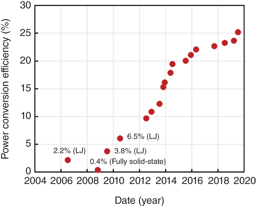
Figure 2.1 Progress of power conversion efficiency (PCE) of halide perovskite‐based photovoltaic cells. LJ indicates liquid‐junction photoelectrochemical cell, in the early days of research.
The highly interdisciplinary nature of the research enabled such rapid progress of PSCs. While solution‐based crystallization of perovskite materials involves a great deal of knowledge and skill in chemistry, optical and electrical characterizations of solid‐state crystals (semiconductors) are based on theories of physics. As a result of this interdisciplinary science, many applications beyond photovoltaics have been found for halide perovskites. One such function is as a high‐performance light emitter. We observed intense green light emissions from spin‐coated thin films of MAPbBr3 under exposure to ambient air at room temperature [8]. Such efficient photoluminescence (PL) of perovskite films is a subject of intense study in fundamental science to assess defect‐induced carrier recombination. At the same time, the enhancement of photoluminescence performance leads to the fabrication of wavelength‐tunable light‐emitting diodes and perovskite‐based lasers.
The fact that halide perovskite has excellent properties does not mean that perovskite PV and optoelectronic devices are ready for industrial use. One of the remaining important issues is ensuring high stability and durability of the perovskite and surrounding carrier transporting materials. To overcome this, considerable efforts are being made in both fundamental research and engineering. In fact, this is the main direction of ongoing research on perovskite‐based devices. The intrinsic stability of halide perovskites is assumed to be due to the nature of their ionic migration, which is a characteristic of metal halide materials as soft ionic semiconductors. Such ionic conductivity is responsible for the peculiar behavior of carrier transports in the perovskites. For example, ionic migration is assumed to cause hysteretic behavior in current–voltage characteristics of the device. Although ion migration is associated with the stability issue, it plays an important role in screening charges (positive and negative) against Coulombic repulsion to stabilize free carriers for long‐range diffusion (>1 μm). Therefore, the question of how to control the behavior of mobile ions by compositional and morphological improvements has become the main focus of study to solve the stability issue.
2.2 Historical Backgrounds of Halide Perovskite Photovoltaics
Research on perovskite materials dates back to 1839 when the Prussian mineralogist and crystallographer, Gustav Rose, discovered the novel material [9, 10]. The perovskite mineral was discovered in the Ural Mountains of Russia by mineral collector August Alexander Kämmerer, who sent the sample to Gustav Rose in Germany for analysis. It was a black mineral composed of calcium titanate (CaTiO3). Kämmerer requested the new mineral be named in honor of the decorated Napoleonic Wars veteran Count Lev A. Perovskiy (1792–1856). Additional information as an interesting story on the discovery of perovskite and collaborations between Russian and German mineralogists has been published as an essay [11]. In 1940s, a high dielectric constant was discovered for an oxide perovskite of BaTiO3. As a ferroelectric ceramic, BaTiO3 has been to date leading the industry of ferroelectrics such as capacitors, superconductors, piezoelectric devices, proton conductors, fuel cells, and memory storage devices [12]. However, oxide‐type perovskites have large bandgaps (>2.5 eV) that lack light harvesting ability and exhibit low efficiency in the collection of free charges. Therefore, metal oxide‐based perovskites do not exhibit good semiconducting properties suitable for photovoltaic absorbers.
Perovskite generally represents a type of crystal structure with the chemical formula ABX3, in which A and B are alkali and metal cations, respectively, and X is an anion (Figure 2.2). In an ideal cubic structure, the B cation has a sixfold coordination, surrounded by an octahedron of anions, and the A cation is in 12‐fold cuboctahedral configuration. The cubic unit cell of such compounds consists of A cations at the cube corner positions, B sitting at the body‐center position, and X anions occupying the face‐centered positions. Before halide perovskites attracted attention as photovoltaic semiconductors, perovskites were generally known as inorganic metal oxides (A = alkali cation, X = oxygen).

Figure 2.2 General crystal structure of perovskite, ABX3.
The class of halide perovskites has halide anions in place of oxide anions (ABX3; A = monovalent cation, B = divalent metal cation, X = halogen anion) and demonstrates the semiconducting properties and strong visible light absorption desired for photovoltaic applications. Discovery of such halide perovskites dates back to the 1890s. In 1893, Wells et al. conducted a comprehensive study on the synthesis of lead halide crystals from solutions including cesium (Cs)‐based CsPbX3 (X = Cl, Br, and I) [13]. In 1957, more than 60 years after the Well's study, Danish researcher Møller found that CsPbCl3 and CsPbBr3 have a perovskite structure [14, 15], showing a tetragonally distorted structure. Later, Weber found that organic cation (CH3NH3+) replaces Cs+ to form CH3NH3MX3 (M = Pb [16] and Sn [17], X = I and Br) and reported the first crystallographic study on organic–inorganic hybrid lead halide perovskites. Toward the end of the last century, the synthesis of a large variety of halide perovskites composed of small and large organic cations was conducted by David Mitzi [18–20]. Mitzi focused his studies on the physical properties of perovskite materials of low‐dimensional structures such as two‐dimensional (2D) perovskites bearing a large organic group [19]. Based on this study, in the late 1990s, Prof. Kohei Sanui was conducting a project through a Japanese national research program (JST‐CREST). This project dealt with self‐organized quantum confinement structures using the above perovskites and conducted detailed investigation on the optical properties of 2D [21, 22] and 3D crystals [23, 24]. Although research opened applications of low‐dimensional perovskite crystals to non‐linear optics and electroluminescence (LED) by utilizing sharp monochromatic optical absorption and luminescence [25, 26], at that time, there was no awareness that these materials could be employed for the utilization of solar energy, which requires a wide spectral absorption to harvest sunlight rather than having a sharp absorption and emission.
During 2005–2006, while we continued putting our efforts toward further development of dye‐sensitized solar cells (DSSCs) [27, 28], we explored the use of organic–inorganic lead halide perovskite as an absorber replacing the organic dye in DSSCs. This research began in 2005 as a collaboration between Toin University of Yokohama (TUY) and Tokyo Polytechnic University (TPU) when Akihiro Kojima, then a graduate student at TPU visited Miyasaka's laboratory to examine the ability of CH3NH3PbX3 to sensitize TiO2 electrodes in a photoelectrochemical cell using a Li halide solution as reducing electrolyte. In 2006, we obtained preliminary results which demonstrated the visible light sensitization of TiO2 with deposited nanocrystals of the perovskite [6]. Assuming that the perovskite would function as a quantum dot‐like sensitizer, deposition of the perovskite was done by spin‐coating with the precursor solution, in which the loading amount of the perovskite was adjusted so as to obtain the thinnest layer of nanocrystalline perovskite, covering a large surface area of a thick TiO2 layer (∼10 μm), similar to the manner of DSSC. This architecture was significantly different from the present PSC that uses a thin TiO2 film (<0.1 μm) as an electron collector (or uses no mesoporous film). After optimizing the cell structure, we fabricated cells that yielded PCEs barely reaching 3.8%. Figure 2.3 shows the performance of perovskite‐based photovoltaic cells published in 2009 [1]. Having also realized the necessity for a solid‐state cell with a solid‐state hole transport material, we attempted to prepare devices by employing a carbon/conductive polymer composite and obtained a low PCE value (<1%). This was the first example of a full‐solid‐state perovskite photovoltaic cell, which we reported in an international conference (electrochemical society [ECS]) in 2008 [29, 30]. We later realized that such poor performance was apparently due to the significantly low loading amount of perovskite, which was also confirmed by Nam Gyu Park and coworkers who improved our method to obtain a higher PCE by simply increasing the perovskite loading [31].

Figure 2.3 (a) SEM image (the scale bar shows 10 nm) of particles (shown by an arrow) of nanocrystalline CH3NH3PbBr3 deposited on the TiO2 surface. (b) IPCE action spectra for photoelectrochemical cells using CH3NH3PbBr3/TiO2 (solid line) and CH3NH3PbI3/TiO2 (dashed line) photoanodes with a liquid electrolyte, 0.4 M LiBr and 0.04 M Br2 dissolved in acetonitrile for the former, and 0.15 M LiI and 0.075 M I2 dissolved in methoxyacetonitrile for the latter photoanode. (c) Photocurrent–voltage characteristics for cells using CH3NH3PbBr3/TiO2 (solid line, PCE = 3.13%) and CH3NH3PbI3/TiO2 (dashed line, PCE = 3.81%) under 100 mW/cm2, air mass (AM) 1.5 irradiation.
Source: Kojima et al. [1].
In 2011, we started a collaborative work with Henry Snaith (H.S.) of Oxford University for creating solid‐state perovskite cells because he had been working on organic hole‐transporting materials (HTMs) for the purpose to solidify the structure of DSSC [32]. THM was spiro‐OMeTAD (2,2′,7,7′‐tetrakis(N,N‐dimethoxyphenylamine)‐9,9′‐spirobifluorene), which was spin‐coated on the perovskite layer. This method finally led to realize the boost of a PCE of up to 10.9% [7]. A surprising feature of the device was the use of an insulating mesoporous Al2O3 as a scaffold for CH3NH3PbI3 crystals. A cell using Al2O3 exhibited higher voltage and PCE than those using TiO2 as scaffold. Indeed, it was an indication of the long diffusion length of carriers in perovskite, which was also indicative from our observation of intense green light photoluminescence (PL) from bromide perovskite (CH3NH3PbBr3) coated on mesoporous Al2O3 [8]. The long carrier diffusion length of the lead halide perovskite, which has been later confirmed by opto‐physical analysis [33] and carrier mobility [34] characterizations, has brought radical changes in our understanding of the functioning of PSCs, distinguishing the new technology from any other organic and hybrid material‐based solar cells. A considerable number of studies, both in chemistry and physics, have been conducted toward improving the quality of solution‐processed perovskite crystalline films and their heterojunction interfaces by reducing the defect density at grain boundaries and interfaces. These monumental efforts have led to the realization of high PCEs of over 25% [35, 36] and a current record PCE of 25.5% [2].
2.3 Semiconductor Properties of Organo Lead Halide Perovskites
The solid‐state physics of halide perovskite semiconductors has been investigated in detail regarding their semiconducting properties, carrier transport mechanisms, and theories of defect‐related charge recombination. Photovoltaic applications have been mainly focused on 3D perovskite materials that perform isotropic carrier transport advantageous for power generation. Unlike conventional semiconductors, halide perovskites are ionic crystals and the semiconducting nature of halide perovskites allows the easy tuning of the bandgap and optical absorption by varying the halide ions. Figure 2.4 shows the wavelength tuning for the I and Br mixture of MA lead halide (CH3NH3Pb(BrxI1−x)3−yCly, 0 ≤ x ≤ 1) [37] and formamidinium (FA) lead halide (HC(NH2)2PbBr1–yIy, y = 0–1) [38]. The absorption edge wavelength corresponding to the bandgap energy changes proportionally with the content of bromide. When iodide is added to the perovskite structure, FAPbBr1−yIy (Figure 2.4e) exhibits a continuous red shift from the edge wavelength of ∼550 nm for pure bromide (FAPbBr3) to ∼830 nm for pure iodide (FAPbI3). A constant emission peak shift similar to that of absorption is also observed in the photoluminescence spectrum. These optical properties corroborate that mixed halide perovskites can form good solid solutions as ionic crystals.

Figure 2.4 (a) Picture of perovskite devices bearing methylammonium lead bromo‐iodide perovskite, CH3NH3Pb(BrxI1−x)3−yCly, (0 ≤ x ≤ 1), films with different Br/I molar ratios on mesoporous TiO2 substrates. (b) Absorption spectra of the perovskite films and (c) their bandgap energies.
Source: (a–c) Suarez et al. [37].
(d) Photographs of formamidinium lead bromo‐iodide perovskite, HC(NH2)2PbBr1−yIy, films with y increasing from 0 to 1 (left to right) and (e) their absorption spectra.
Source: (d, e) Eperon et al. [38].
Strong bandgap absorption at the edge wavelength and broad flat absorption covering visible light wavelengths indicates that halide perovskites work as excellent absorbers for sunlight. MA lead halide iodide (MAPbI3), which is a standard perovskite absorber in photovoltaic cells, can be characterized as a rare intrinsic semiconductor [39] exhibiting the excellent mobility of both photogenerated electrons and holes. Density functional theory (DFT) and first principles theory‐based calculations have corroborated the superior photophysical properties of MAPbI3, which has long diffusion lengths for free carries. Figure 2.5 shows the lattice structure of MA halide perovskite, MAPbX3 (X = I, Br, and Cl), and the band structures of MAPbI3 based on studies by Kondo et al. [41] and Brivio et al. [40]. The valence band (VB) of MAPbI3 consists of approximately 70% of I 5p orbitals and 25% of Pb 6s2 orbital (lone pair), whereas the conduction band (CB) consists of a mixture of Pb 6p and other orbitals. Here, VB orbitals have a strong coupling between Pb lone‐pair 6s2 and I 5p orbitals [42]. This structure is opposite to that of GaAs, in which VB and CB are formed by p and s orbitals, respectively. Here, an important feature of the electronic structure is that both CB and VB consist of antibonding orbitals.

Figure 2.5 (a) Structure of organo‐metal halide perovskite crystal. (b) Bandgap structure and energy levels of CH3NH3PbI3. (c) Electronic structure of CH3NH3PbI3 based on the quasiparticle self‐consistent GW approximation. Zero denotes the valence band maximum. Green and red solid lines depict bands of I 5p and Pb 6p, respectively, and light‐gray dashed lines show corresponding bands in local-density approximation (LDA).
Source: Brivio et al. [40].
The high symmetry and direct bandgap of MAPbI3 and the p–p electronic transitions from VB to CB, enabled by the Pb s orbital lone pair, contribute to the high optical absorption coefficients of this material (105 cm−1) [43]. The unique defect properties of perovskite are attributed to strong Pb s–I p antibonding coupling, weak Pb p–I p coupling, and ionic characteristics [42]. Weak antibonding coupling between Pb p and I p orbitals fixes the conduction band minimum (CBM) close to the Pb p orbital, and strong Pb s–I p antibonding coupling lowers the valence band maximum (VBM) close to the I p orbital. Therefore, for vacancies (defects) formed by the removal of I−, the defect state lies between the Pb p atomic orbital level and CBM level, and for Pb2+ vacancies, the defect state is formed between the I p and VBM levels. Hence, unlike other ionic semiconductors, where localized nonbonding orbitals surrounding the ion vacancies form trap states deep within the bandgap, such defects in perovskites (MAPbI3) generate trap states that either reside within the bands (VB or CB) or exist as shallow traps near the CB and VB. Carriers trapped in shallow defects can be easily detrapped and contribute to current generation. This explains the rare nature of perovskite semiconductors attributed with “defect tolerance”. The defect tolerant nature of perovskite is reflected by large carrier diffusion lengths as measured by photoluminescence (PL) lifetime, which are in the range of 1 μm (polycrystalline film) [33] to over 100 μm (single crystal) [34]. Furthermore, as MAPbI3 is an intrinsic semiconductor, the mobility of its carriers is ambipolar, exhibiting a similar effective mass for both electrons and holes (0.23–0.29) [44]. Similar to inorganic photovoltaic semiconductors such as Si and GaAs, photogenerated carriers in MAPbI3 behave as free carriers and these carriers can migrate without recombination for as long as several hundreds of nanoseconds, as shown in PL measurements [33, 45, 46]. It is also considered that the high ionic density in halide perovskites helps to suppress charge recombination by a charge‐screening effect against Coulombic interactions.
In summary, the important factors that support superior performance and high efficiency of PSCs are (i) high optical absorption coefficient (105 cm−1) that allows the use of thin films (<0.5 μm), (ii) long carrier diffusion length and suppressed recombination (defect tolerance), and (iii) well‐balanced charge transfer. In photovoltaic applications, the defect tolerant nature of halide perovskite is especially important and leads to the generation of high voltage. The high PCE of PSCs is a result of high photovoltage (1.1–1.2 V) output rather than the amplitude of the photocurrent [47]. The open‐circuit voltage (VOC) of all types of existing solar cells undergoes a large thermal loss from its bandgap energy (eV). Such a voltage loss (VOC deficit) often constitutes more than one‐third of the bandgap energy (Eg). Perovskite solar cells of high efficiency usually generate VOC exceeding 1.1 V or in the best cells over 1.2 V (1.26 V obtainable with MAPbI3 [48]) with respect to their Eg of 1.55–1.6 eV. Figure 2.6 shows the average values of the VOC deficit (Eg/e−VOC) for different types of solar cells. The lowest value of the deficit is obtained for a single crystal of GaAs which, as a single‐junction solar cell, is known to present the highest PCE value of 27.8%, exceeding the top PCE of crystal silicon (26.1%). With an Eg of 1.42 eV, the GaAs cell is capable of VOC up to 1.12 V. This small deficit, 0.3 eV, is close to the Shockley–Queisser theoretical limit [49, 50]. Compared with GaAs, semiconductors of perovskites and their solar cells are also superior in reducing the VOC deficit to the range of 0.35–0.45 V.

Figure 2.6 Power conversion efficiencies of solar cell as a function of bandgap energy (a) with Shockley–Queisser limit values in dotted line. Average values of VOC deficit (Eg/e−VOC) for different kinds of solar cells (b).
2.4 Working Principle of Perovskite Photovoltaics
Although mesoporous metal oxides such as TiO2 and Al2O3 serve as a scaffold for holding perovskite nanocrystals, the perovskite photovoltaic device can work even without a mesoporous scaffold layer (planar heterojunction with compact TiO2 layer for collecting electrons). This makes it clear that the PSCs work more like solid‐state p–n junction solar cells in which perovskite works as an intrinsic semiconductor (i) sandwiched between two selective (p and n) contacts. In the n–i–p structure, typically TiO2 is used as an n‐type electron transport material (ETM) and a HTM such as spiro‐OMeTAD is used as a p‐type contact. Here, a typical device structure using transparent conductive electrodes such as F‐doped tin oxide (FTO) or indium tin oxide (ITO) comprises a junction of FTO(ITO)/TiO2/perovskite/spiro‐OMeTAD/metal. In a p‐i‐n type structure, which is otherwise known as an inverted structure, perovskite is sandwiched by a p‐type material (e.g. conductive polymers such as PEDOT‐PSS) at the bottom and an n‐type layer (e.g. fullerene derivative such as PCBM) at the top, forming a junction of FTO(ITO)/PEDOT‐PSS/perovskite/PCBM/metal. Some typical architectures of PSCs are illustrated in Figure 2.7. The perovskite absorbs light to generate electrons and holes, and electrons are selectively collected by the n‐type ETM layer, while the holes are collected by the p‐type HTM layer. Electrons flow through the external circuit to reach the p‐type layer to combine with the holes. Figure 2.8 shows the band diagram of a typical metal oxide ETM‐based perovskite device (FTO/TiO2/perovskite/spiro‐OMTAD/Au).

Figure 2.7 Variety of layered architectures for perovskite solar cells. (a) Mesoscopic n–i–p with semiconductor metal oxide. (b) Mesoscopic n–i–p with insulating metal oxide scaffold. (c) Planar n–i–p. (d) Planar n–i–p (inverted). (e) ETL‐free. (f) HTM‐free. (g) HTM‐free carbon electrode.
Source: Jena et al. [3].

Figure 2.8 Energy diagram of a typical perovskite solar cell using MAPbI3 as the perovskite absorber, TiO2 as the ETM, and spiro‐OMeTAD as the HTM. FTO and Au are front and back contacts, respectively.
Source: Jena et al. [3].
An important factor that leads to the high PCE of PSCs is the open‐circuit voltage (VOC). The VOC of some perovskite cells (1.18–1.26 V) [48, 51] approaches the Shockley–Queisser theoretical limit of VOC (∼1.32 V) based on the bandgap of the perovskite semiconductors (1.6 eV for MAPbI3) [52, 53]. In photovoltaic cells, VOC is generally determined by the energy gap between the Fermi levels of selective contacts, namely, p‐type and n‐type conductive layers. For the typical junction structure in Figure 2.8, these contacts are given by spiro‐OMeTAD as the HTM and by TiO2 as ETM, their energy gap corresponds to the difference between the highest occupied molecular orbital (HOMO) level of HTM and the CB level of TiO2. Although FTO and Au as conductive electrodes have their own work functions, their energy gaps have little influence on VOC because of their low charge selectivity. Furthermore, the CB level of the TiO2 ETM tends to have less of an effect on controlling the energy gap that determines the maximum value of VOC. This tendency is apparent when TiO2 is replaced with SnO2. Despite the low CB level of SnO2 (approximately 0.25 eV lower than that of TiO2), comparably high VOC (>1.0 V) can be obtained using both ETMs [54, 55]. This fact may indicate that mesoporous metal oxides (TiO2 and SnO2) mainly function as scaffolding for perovskite crystals, and the material that primarily serves as an ETM is a thin compact oxide layer (general thickness <10 nm) that covers the surface of the FTO below the mesoporous layer. However, such a compact layer is considered to be too thin to exhibit the semiconductor property, although it is capable of rectifying electron transfer at the interface by blocking hole injection. As a result, the energy gap that relates to the value of VOC is assumed to be the difference between the CB level of the perovskite absorber and the HOMO level of the HTM.
Theoretical modeling of the electronic structures of MAPbI3 shows that the defect formation influencing carrier recombination is limited to energetically shallow positions near the CB and VB levels rather than deep defects in the bandgap that strongly trap carriers. Material simulation based on first principles theory suggests that such a superior structure is unique to lead iodide‐based compositions [42] and is difficult to realize for other metal halide semiconductors. At the time of this review, the only non‐lead halide perovskites able to increase PCE beyond 10% are tin (Sn)‐based perovskites, which have electronic structures similar to lead halide perovskites and absorb visible light and near‐infrared light. Unlike the single crystals of perovskite, solution‐processed thin films of perovskites are composed of aggregates of nanocrystalline perovskite particles with dispersed grain size and the large number of defects formed on the grain surface and boundaries substantially influence the photovoltaic properties. Hence, it is essential to minimize the defect density at the grain surface and boundaries by chemically modifying the molecular structure of perovskite at the contact interface. Chemical engineering for this purpose, such as increasing the grain size (decreasing the boundary area), improving the uniformity of film morphology, and passivating the defects using additives, not only enhances the photovoltaic performance but also improves the stability of the perovskite films.
2.5 Compositional Design of the Halide Perovskite Absorbers
Incorporation of different cations in the A site and different halides in the B site influences on both efficiency and stability. A certain mix of cations at the A site and halides at the B site demonstrated superiority over single cation/halide perovskites. The most popular organic cation MA has the issue of thermal stability because of physical evaporation of this small molecule at temperatures above 120° C [56]. In this aspect, the current high‐stability development of perovskite PV cells tends to choose MA‐free compositions [55] and/or all inorganic compositions [57]. Based on the ionic size and geometrical tolerance factor (τ), which is an empirical index widely used for predicting perovskite crystal structure (see Section 2.6), combinations of different cations such as MA, FA, Cs, Rb, and anions (I, Br, Cl) have been explored. Out of all possible combinations [58], the mixed perovskite that has become most popular in recent years is (MA/FA/Cs)Pb(I/Br)3, which is known as triple cation perovskite. The quadruple cation‐based perovskite, which includes Rb (i.e. (MA/FA/Cs/Rb) Pb(I/Br)3) as the fourth cation, has also gained interest owing to its high cell efficiency and stability. Here, small inorganic cations such as Cs and Rb are expected to contract the lattice and thus increase the bandgap energy (Eg), while large organic cations such as FA+ expand the lattice and decrease the Eg. FA+, having a larger ionic radius (r = 0.253 nm) than MA+ (r = 0.217 nm), expands the crystal a small amount, resulting in decreased PbI bond distance, which eventually lowers Eg. Pure FAPbI3 shows an Eg of 1.47 eV, while that for pure MAPbI3 is 1.55 eV. With an extended absorption edge (>800 nm), FAPbI3 cells show a larger short‐circuit photocurrent (Jsc) that leads to a PCE of over 20% [59]. MA and FA affect the intrinsic stability of perovskites. MAPbI3 is fairly stable in its crystal structure temperatures below 120 °C. However, FAPbI3 readily crystallizes into a photo‐inactive phase (δ‐FAPbI3) at room temperature, while this phase is transformed to the photoactive black phase (α‐FAPbI3) at high temperatures (125–165 °C) [60]. Such phase instability often affects the photovoltaic characteristics by reducing the FF of FAPbI3. Despite the phase instability, the thermal stability of FAPbI3 is significantly greater than that of MAPbI3 [56]. FAPbI3, when heated at 150 °C for hours, does not change color, whereas MAPbI3 becomes yellow (due to the formation of PbI2) at 150 °C (or even lower) for just 30 minutes [38]. Such thermal stability is attributable to the increased tolerance factor and stronger interaction of FA with iodide ions. The partial replacement of MA with FA also significantly improves the thermal stability of MAPbI3. Substitution of a certain amount of MA with Cs also improves efficiency and thermal stability simultaneously. As reported by Niu et al. [61], 9 mol% of Cs in CsxMA1−xPbI3 (x = 0.09) showed better performance and thermal stability than pristine MAPbI3. Cs inclusion also enables stabilization of FAPbI3. Small and large tolerance factors, respectively, for CsPbI3 (τ = 0.85) and FAPbI3 (τ = 0.98) stabilize the perovskites in orthorhombic and hexagonal structures, respectively, both of which are yellow due to the formation of PbI2 and not active in photovoltaic function. However, an effective tolerance factor can be tuned to form a cubic structure (0.9 ≤ τ ≥ 1) by alloying CsPbI3 with FAPbI3 (FAxCs1–xPbI3) over a range of proportions. Structural/phase stability and the cell performance of FAPbI3 are also improved by mixing 10–20% of Cs. For example, FAPbI3 perovskite thin films, when exposed to a humid environment for 15 days, show continuous degradation, while the addition of 15% of Cs to the film (FA0.85Cs0.15PbI3) sustains performance of the device without reduction of efficiency [62]. These studies led to develop high efficiency and stable cells by using MA‐free CsFA cation‐based perovskites as hybrid absorbers. Recently, Rb‐doped CsFAPbI3 perovskites were used to fabricate highly durable PSCs (PCE > 20.3%) which can function for 1000 hours under continuous sunlight exposure [55].
2.6 Strategy for Stabilizing Perovskite Solar Cells
The performance of the PSCs is reaching the theoretical limit (SQ limit) in terms of the fill factor and output voltage [35, 36]. However, these high PCE record values are not compatible with sufficiently high stability of the device in most cases. This is different from the case of commercialized high‐performance devices using inorganic photovoltaic (PV) semiconductors such as Si, GaAs, and CdTe, which can sustain high stability compatible with high efficiency. The instability of halide perovskite materials under high temperature and continuous irradiation is ascribed to the ionic mobility intrinsic to the ionic semiconductors in which highly diffusible halide anions are largely responsible for the instability. Ionic diffusion is also assumed to cause anomalous hysteretic behavior of the photocurrent in I–V performance [63, 64], which can be enhanced in the presence of structural defects or voids at the interface of the perovskite and charge transport layers [65, 66]. Despite these drawbacks, the strong ionic character of the metal halide structure contributes to stabilizing free carriers via the charge screening effect, which is assumed to enable excellent PV performance of the halide perovskite. Therefore, stability and high performance often have a trade‐off relationship. To overcome this dilemma, compositional engineering should be directed to not only create the perovskite composition that can reduce the ion diffusion but also to modify the chemical structure of heterojunction interfaces where mobile ions can diffuse beyond the interfaces to interact with the adjacent layers. Simultaneous improvement of efficiency and stability has also been achieved by improving the morphology and physical quality of solution‐processed perovskite films. While the use of large grains and high crystallinity of perovskite enable high efficiency, large grains and a dense uniform morphology are advantageous for improving the stability. Figure 2.9 shows an example of a high‐efficiency (>21%) triple cation PSC fabricated under ambient conditions in our laboratory [67]. This large‐grain perovskite film maintains its high PCE for storage of the cell exposed to ambient air for more than five months.

Figure 2.9 Cross‐sectional SEM image (a), J–V curves (b), and PCE histogram plot (c) of triple cation perovskite solar cells fabricated in ambient air under controlled humidity (15–25%).
Source: Based on Singh and Miyasaka [67].
The triple‐cation recipe was then followed by a quadruple‐cation mixed perovskite that included Rb as the fourth cation. With the mixed perovskite composition (5% of Rb, bandgap of 1.63 eV), Saliba et al. achieved stabilized efficiencies of up to 21.6% and the polymer‐coated cells maintained 95% of their initial performance during 500 hours of operation at the maximum power point at 85 °C [68]. In comparison to Cs/FA/MA triple cation devices, Rb‐based quadruple‐cation perovskite cells show greater photostability, which can be attributed to reduced recombination and fewer defects [69].
Practical durability issues with perovskite include both intrinsic and extrinsic stability. Here, extrinsic stability is affected by environmental stresses such as heat, light, humidity, and oxygen. The intrinsic structural stability of perovskites can be primarily determined by the Goldschmidt tolerance factor (τ) of the crystal, where ![]() and r is the ionic radius. The value of τ varies with the size of the ions in ABX3. Since the ionic radii of organic cations (A) cannot be determined accurately, a certain amount of uncertainty lies in the calculated tolerance factors. Figure 2.10 shows the calculated tolerance factors of APbI3 systems where A = Na, K, NH4, Rb, Cs, MA, FA, EA (ethylamine), and EDA (ethylenediamine). When τ is in the range of 0.8 < τ < 1, ideal cubic perovskite structures or distorted perovskite structures with tilted octahedra are favored. Specifically, 0.9 < τ < 1 favors a cubic perovskite structure, while for 0.8 < τ < 0.9, a distorted perovskite structure is formed. Values of τ < 0.8 and τ > 1 diminish the possibility of the formation of perovskite structures. Therefore, it can be expected that τ close to the middle of the range from 0.8 to 1, away from both the non‐perovskite zones, would form a stable perovskite [70]. For FAPbI3, τ is close to 1, which is near the upper boundary of the perovskite structure; therefore, FAPbI3 is prone to the formation of a hexagonal δ‐phase, which is photoinactive. An all‐inorganic composition, CsPbI3, with τ ∼ 0.8, is at the edge of the lower boundary for perovskite structures and normally crystallizes into a δ‐phase. MAPbI3 with τ ∼ 0.9 is close to the middle of the perovskite zone and forms a black photoactive perovskite phase.
and r is the ionic radius. The value of τ varies with the size of the ions in ABX3. Since the ionic radii of organic cations (A) cannot be determined accurately, a certain amount of uncertainty lies in the calculated tolerance factors. Figure 2.10 shows the calculated tolerance factors of APbI3 systems where A = Na, K, NH4, Rb, Cs, MA, FA, EA (ethylamine), and EDA (ethylenediamine). When τ is in the range of 0.8 < τ < 1, ideal cubic perovskite structures or distorted perovskite structures with tilted octahedra are favored. Specifically, 0.9 < τ < 1 favors a cubic perovskite structure, while for 0.8 < τ < 0.9, a distorted perovskite structure is formed. Values of τ < 0.8 and τ > 1 diminish the possibility of the formation of perovskite structures. Therefore, it can be expected that τ close to the middle of the range from 0.8 to 1, away from both the non‐perovskite zones, would form a stable perovskite [70]. For FAPbI3, τ is close to 1, which is near the upper boundary of the perovskite structure; therefore, FAPbI3 is prone to the formation of a hexagonal δ‐phase, which is photoinactive. An all‐inorganic composition, CsPbI3, with τ ∼ 0.8, is at the edge of the lower boundary for perovskite structures and normally crystallizes into a δ‐phase. MAPbI3 with τ ∼ 0.9 is close to the middle of the perovskite zone and forms a black photoactive perovskite phase.

Figure 2.10 Calculated tolerance factors (τ) for different cations (A) in an APbI3 perovskite system. Commonly used cations like Cs, MA, and FA present τ in the range of 0.8–1.0, indicating the cubic perovskite phase structure. Ionic sizes of A cations used in calculation are values referring to XII coordination, not VI coordination. Ethylammonium (EA) and ethylenediamine (EDA) cations are too large, giving rise to τ values >1.0 and thus fall into the “upper forbidden zone” and cannot form perovskite alone. The group I alkali metal cations (Na, K, and Rb) and NH4 have a τ value <0.8 and fall into the “lower forbidden zone,” not forming perovskite. However, all cations of lower or upper “forbidden zones” can be used as additives into those cations in “cubic perovskite formation zone” for phase stabilization.
Source: Jena et al. [3].
The compositional engineering of perovskite by mixing different cations and anions improves the structural stability of perovskites, essentially by adjusting the value of τ close to the middle of the perovskite zone. The addition of Cs or MA to FAPbI3 moves the τ value down from 1 to stabilize the cubic phase of FAPbI3. The effective tolerance factor (τeff) of a mixed perovskite, (MAPbBr3)0.15(FAPbI3)0.85, calculated using the values of rA(eff) for MA and FA and rX(eff) for halogen is ∼0.98, while that for triple‐cation mixed perovskite with 5% Cs (i.e. Cs0.05(MA0.17FA0.83)0.95Pb(I0.83Br0.17)3) is ∼0.97. From such values of τeff, it can be predicted that more Cs or MA in these mixed perovskite systems should result in even more stable perovskite structures. However, τeff close to 0.9 is not a sufficient condition for predicting the structural stability of mixed perovskites. The crystal structure difference between MAPbI3 (tetragonal) and mixed perovskites (FA‐MA‐Cs) (usually cubic) might also explain why mixed perovskites are more stable. As cubic structures with higher symmetry than tetragonal structures are more stable, mixed perovskites with cubic structures show better stability than pure MAPbI3. Moreover, the thermodynamic stability of perovskite structures depends on the halide composition. At high temperatures, MAPbX3 (X = Cl, Br, and I) decomposes into PbX2(s), MA(g), and HX(g). The energy of formation of these component products of the degradation process confirms that MAPbI3 and MAPbBr3 are thermodynamically more stable than MAPbCl3 [71]. Structural stabilities of mixed‐cation perovskites are summarized in review articles [72]. Furthermore, a recent analysis of the multi‐cation perovskite decomposition process has confirmed that Cs inclusion increases the thermal stability of FA0.85MA0.15 Pb(I,Br)3 perovskite [73].
Ion migration in the halide perovskite crystal also triggers the degradation of materials. It can cause anomalous photocurrent–voltage (J–V) hysteresis, phase segregation, and deterioration of the long‐term stability of PSCs. It is believed that ions in perovskites essentially migrate through the cation and anion defects (i.e. MA+ and I− vacancies). Calculation of activation energies of migration for different constituting ions (i.e. I−, Pb2+, and MA+ of FA+) in perovskites suggests that iodide is the most easily migrating ion [74], which is consistent with experimental studies [75]. MA+ cations also migrate in perovskite crystals [76]. In polycrystalline films, the preferred regions of ion migration are considered to be grain boundaries rather than within the grains. Therefore, it is possible to minimize ion migration by reducing the number of grain boundaries or by increasing the grain size.
In addition to the intrinsic stability of perovskites, the stability of perovskite‐based devices is affected by external conditions such as moisture, oxygen (air), heat, light, and external bias, which can degrade the device structure involving the change of surrounding carrier transport materials. Because ionic conductors have some affinity for polar media, the sensitivity of perovskite to moisture (H2O) has been a matter of concern for its long‐term stability. It is known that water molecules easily bind to perovskite by hydrogen bonding to form hydrated compounds, which alter the properties of perovskite locally. The losses caused by these hydrated compounds can be reversed, as shown for MAPbI3 in Eq. 2.1, but further ingression of water can cause irreversible degradation of perovskite to PbI2 and other components (Eq. 2.2) [77].

Therefore, the proper encapsulation of PSCs with films of gas barrier functions is a prerequisite for the prevention of degradation caused by moisture. On the other hand, many efforts have been made to improve the moisture resistance of materials constituting the cell structure, either by introducing hydrophobic layers such as polymer/carbon composites in place of the widely used spiro‐OMeTAD [78], or by incorporating non‐hygroscopic interlayers between perovskite and HTM [79, 80], or by passivating (modifying) the perovskite surface with small molecules [81]. For instance, tetra‐ammonium zinc phthalocyanine has been employed to passivate the grain boundary of MAPbI3 [82], and the stabilized device showed a long lifetime of 1000 hours sustaining 90% of PCE for storage at 85 °C and 45% humidity.
A recent major trend in modifying the surface and grain boundaries of perovskite films is to incorporate a 2‐dimensional (2D) perovskite material with a hydrophobic organic group into the general 3‐dimensional (3D) perovskites [83]. The method serves two purposes: passivation of the traps and protection against moisture ingression. Large organic cations in 2D perovskites are more hydrophobic than MA and FA and help to increase the moisture resistance. For instance, the incorporation of 0.8 mol% of ethylenediammonium iodide (EDAI) (which forms a 2D perovskite structure EDAPbI3 when mixed with PbI2) into a 3D MAPbI3 structure improves the PCE by reducing recombination [84] and enables stable operation of the device at 50 °C and 50% relative humidity under illumination. Similarly, phenylethylamine iodide (PEAI) was employed to deposit PEA2PbI4 capping layers on top of the 3D perovskite film, which improved the long‐term stability of the cell, retaining nearly 90% of the initial PCE (around 18%) after 1000 hours exposure in ambient conditions with a relative humidity of 60 ± 10% [85]. The hydrophobic nature of the trifluoroethylamine (FEA) chain was applied to incorporate 2D perovskites in triple‐cation 3D perovskite, (FA0.825MA0.15Cs0.025) Pb(I0.85Br0.15)3, to reinforce moisture resistance [86]. A cell using FEA‐modified perovskites without encapsulation maintained over 90% of the initial PCE (18%) under a humidity of 65% at room temperature for up to approximately 28 days. FEA‐based 2D perovskite, (FEA)2PbI4, was also introduced at the interface of perovskite and HTL to protect FA0.85MA Pb(I0.85Br0.15)3 from moisture erosion and stabilize the cell under 50 ± 5% humidity for 60 days [87]. Alkyl diammonium‐based perovskites can serve as a 2D perovskite interlayer to bridge 3D perovskite layers [88]. Butanediamine iodide (BEAI2) was employed to passivate the grain boundaries of perovskites by vapor phase post‐treatment and improved ambient stabilities of the high‐performance cell (PCE > 19%) at a high temperature (85 °C) and under continuous illumination [89]. One 2D material, 5‐aminovaleric acid iodide (AVAI), has become a popular material for stabilizing MAPbI3 since it has been employed in dopant‐free carbon‐based PSCs [90]. Three mole percent of AVAI added to MAPbI3 perovskite stabilizes a carbon‐based PSC device, and a large module (10 × 10 cm2) of the device exhibited stability for more than 10 000 hours (>1 year) at 55 °C under 1‐sun illumination [91]. Carbon‐based PSCs have relatively high thermal stability owing to the use of dopant‐free chemically stable carbon layers. The recent progress of carbonaceous material‐based PSCs is summarized in a review [92].
The moisture resistance of PSCs can also be enhanced by modifying the perovskite surface with hydrophobic polymers. For instance, an ultra‐thin layer (<10 nm) of polyvinylpyridine (PVP) coated on the perovskite surface (MAPbI3) and in contact with spiro‐OMeTAD improves the water resistance of MAPbI3 when dipped in water for up to 100 seconds [79]. A similar result was also reported by Tress and coworkers who found a large effect of suppressing nonradiative recombination using PVP as a thin interlayer and succeeded in elevating VOC to 1.20 V [93]. Furthermore, the continuous chemical functionalization of the grain boundaries of MAPbI3 films by using triblock copolymers that exhibit both hydrophilicity and hydrophobicity has also been found to boost the PCE as well as the stability of MAPbI3 cells [94]. Hence, surface modification using 2D perovskites and hydrophobic polymer materials can dramatically raise the moisture resistance.
Influence of light on the stability (photo‐instability) of perovskite is becoming a formidable issue. Almost all chemical processes such as ion migration, defect generation, and phase segregation, which affect the long‐term stability of perovskites, are unfortunately found to be influenced by light, which must inevitably shine on the cells for their operation. Photocatalytic degradation by TiO2 [95], photoinduced ion migration [96], photoinduced trap state generation [97], and photoinduced phase segregation [98] have been found to be the reasons for performance deterioration under constant illumination. UV light‐induced photocatalytic degradation by the most widely used ETM, TiO2, can be prevented by replacement of TiO2 with an alternative, less photoactive ETL such as SnO2. However, photoinduced phase segregation or ion redistribution in mixed halide (I and Br) perovskites is a serious issue to be solved. A reversible photoinduced phase separation results in the formation of iodide‐rich and bromide‐rich regions [99] in mixed‐halide perovskites. Such I‐rich and Br‐rich phase separation leads to the generation of low‐bandgap trap states, which causes performance degradation of the solar cells under illumination. It is believed that defects such as halogen vacancies are essentially the main promoters of such phase separation. As ion mobility in these materials is known to be more facile at the grain boundaries [100], reducing the volume of grain boundaries (growing large grains) by compositional tuning with Cs or FA results in improved photostability by slowing down ion migration. Phase segregation can be ignored using pure mono‐cation/anion compositions such as MAPbI3, FAPbI3, CsPbI3, etc. In this regard, the use of MAPbI3, which is relatively stable at room temperature and against humidity, is still promising if the device is perfectly protected by encapsulation.
Finally, carrier‐transporting materials that contact the perovskite layer also play a substantial role in changing the device stability. The HTM can be very critical for long‐term stability because perovskite/HTM junctions are the “beating heart” of the whole device. Spiro‐OMeTAD is an excellent HTM in terms of appropriate HOMO levels and is useful as a relatively thick film prepared by simple coating. However, spiro‐OMeTAD requires mixing of ionic dopant (lithium bis(trifluoromethanesulfonyl)imide, Li+TFSI−, etc.), which promotes the oxidation of this HTM under ambient air to ensure normal hole conductivity. Such dopants, owing to their hygroscopic nature, allow the easy ingress of moisture into the film, which eventually degrades the perovskite film (turning yellow). Furthermore, ionic dopants diffuse to the perovskite layer across the junction interface and trigger deterioration of the device performance. Such diffusion can be accelerated at high temperatures or under ambient humidity. It is known that the spiro‐OMeTAD layer undergoes deformation by generating many voids inside the layer upon heating to 100 °C [101, 102]. The mechanism of device degradation includes not only the dopant diffusion of HTM but also ionic migration from perovskites. For example, Carrilo et al. reported that spiro‐OMeTAD+ can react with migrating I− to reduce hole conductivity of the HTM [103]. Zhao et al. found that MA+ ions from MAPbI3 can diffuse into spiro‐OMeTAD and, thereby, cause performance degradation [104]. Therefore, the prevention of ion diffusion between the layers is one of the strategies to improve the thermal stability of PSCs. Apart from instability, another problem of spiro‐OMeTAD is high cost of the material. To replace spiro‐OMeTAD, a great deal of effort has been made to synthesize various types of organic HTMs for use in PSCs [105]. These HTMs are either small molecules or hole‐conducting (p‐type) polymers. Conducting polymers are represented by P3HT, PTAA, PEDOT:PSS, etc. PTAA has been employed to record the highest efficiency of PSCs [106]. However, organic HTMs, including these polymers, are intrinsically low in conductivity and require the use of p‐dopants and/or additives similar to spiro‐OMeTAD. Therefore, their dopants still retain the risk of lowering the device stability.
A solution to avoid the degradation caused by organic HTMs is to develop a dopant‐free HTM bearing no ionic moieties in its structure. Inorganic HTMs have been studied to replace organic HTMs. They are p‐type oxide or compound semiconductors such as NiOx, CuOx, Cu2O, CuI, Cu(thiourea)I, CuSCN, CuGaO2, CuCrO2, and Cu phthalocyanine. Promisingly, many of them have achieved comparable efficiency and longer life than spiro‐OMeTAD. Aside from these inorganic HTMs, the development of dopant‐free organic HTMs is becoming a main strategy to stabilize PSCs. Although organic HTMs are thermally less stable than inorganic HTMs, they can have higher chemical and electrochemical stabilities than inorganic materials against oxidation. Among small molecules alternative to spiro‐OMeTAD, a truxene core‐introduced OMeTAD derivative achieves a high PCE of 18.6% without the addition of dopants and a long lifetime of the device for 33 days of storage [107]. Cao et al. employed a spiro‐based dopant‐free HTM containing redox‐active triphenyl amine units that achieved a high PCE of 20.6% [108]. Donor–π–Acceptor‐type (D–π–A) molecules have been developed for new HTMs in which intramolecular charge transfer nature of the D–π–A molecule is assumed to eliminate the need for dopants. Nazeeruddin and coworkers reported that an HTM consisting of a quinolizino acridine donor and terthiophenes and malononitriles as acceptors gave a PCE of 18.9% with superior long‐term stability under 1300 hours illumination [109]. Phthalocyanine (Pc) derivatives are known as robust organic pigments and p‐type semiconductors. They also work well as dopant‐free HTMs with excellent moisture resistance and high thermal stability [110]. For example, a thin film (about 40 nm in thickness) of a butyl derivative of copper Pc (CuPc) was coated on a high efficiency perovskite absorber (Cs0.07Rb0.03FA0.765MA0.135PbI2.55Br0.45) by solution process and achieved PCE values exceeding 20%. While the above small‐molecule dopant‐free HTMs exhibit high efficiency, the use of polymer HTMs is also sought because of their hydrophobic nature to ensure moisture resistance in addition to good thermal stability. Dopant‐free polymer HTMs with high solubility would be one of the best choices of HTMs. Unlike poly‐triarylamine (PTAA)‐type polymers, which work at high efficiency with dopants, these dopant‐free polymer HTMs are mostly based on thiophene backbone chains, similar to the structure of P3HT [105]. For example, a dopant‐free copolymer comprising ethylhexyloxy phenylene and bithiophene units, which was employed in a PSC device with an inverted structure, showed a PCE of 19.5% (certified) [111]. Park et al. have employed D–A‐type copolymers (asy‐PBTBDT) comprising benzo‐dithiophene and benzothiadiazole (BT) as donor and acceptor units, respectively. Their dopant‐free devices yielded PCEs up to 19.8% with a high VOC of 1.14 V [112]. Reflecting on the effect of polymer HTMs as protective layers, most of these polymer HTM‐based PSCs have a shelf life of more than 30 days under ambient air. A new dopant‐free copolymer was recently developed in our group. Comprising 2,5‐pyrroledione and bithiophene units, an alternating copolymer poly(DTSTPD‐r‐BThTPD), has a high hole mobility of 1.5 × 10⁻³ cm2/(V s) and is thermally stable up to 330 °C [113]. This dopant‐free polymer exhibited high VOC performance for all‐inorganic PSCs using CsPbI2Br as an absorber, whose HOMO level is located at approximately −5.58 eV, slightly lower than that of the HTM (Figure 2.11). The dopant‐free CsPbI2Br solar cell yielded a PCE of 15.5% according to its bandgap of 1.92 eV (wider than 1.73 eV of CsPbI3), but achieved a significantly high VOC value of 1.43 V [114]. Combination of these dopant‐free and high‐efficiency HTMs and 2D‐based stabilization of perovskite compositions is expected to realize development of high‐performance and robust PSCs toward device implementation.

Figure 2.11 Polymer hole‐transporting materials (HTMs). A thin film (20–40 nm) of THM coated on the perovskite CsPbI2Br layer (a) and the relation of polymer HTM energy levels with respect to CsPbI2Br (b).
Source: Öz et al. [113].
2.7 All Inorganic and Lead‐Free Perovskites
The design of organic‐free (all‐inorganic) compositions for photovoltaic absorbers can be a way to guarantee the thermal robustness of the device. Cs‐based lead perovskites have been extensively studied for this reason. Although Cs perovskites show stability at high temperatures, CsPbI3 undergoes chemical equilibrium changes depending on the temperature. For example, the photovoltaically active black phase of α‐CsPbI3 (cubic) can be stabilized at temperatures above 310 °C [115], while the inactive yellow phase δ‐CsPbI3 (orthorhombic) tends to dominate the crystal at room temperature. Furthermore, CsPbI3 absorbs moisture due to its hydrophilic nature. Despite this difficulty, the PCE of CsPbI3 PSCs has increased from 2.9% in the very first experiment by Snaith and coworkers [115] in 2015 to 18.4% in a recent work undertaken by Wang et al. [116], who found that the β‐phase (tetragonal) of CsPbI3, which is a photoactive black phase (bandgap, 1.68 eV), can be stabilized at room temperature. There are other ways to stabilize the black active phase by introducing 2D‐perovskite such as ethylene diamine lead iodide (EDAPbI4) [117]. We found that the inclusion of Eu2+/3+ into CsPbI3 can stabilize the black α‐CsPbI3 phase at room temperature by reducing the grain size [118]. An additional research direction for Cs‐based inorganic perovskites is to enhance the photovoltaic functions of Br‐mixed CsPbI3, which have wider bandgaps depending on the fraction of Br/I. Br substitution in CsPbI3 lowers the black phase formation temperature from 350 °C to about 250 °C and improves stability against phase transition. Although pure CsPbBr3 having a wide bandgap of ∼2.3 eV is not suitable for a sunlight absorber, bromoiodide perovskites CsPbI3Br3−x with narrower bandgaps show promise for application in the top cell of tandem solar cells or indoor photovoltaic cells. In particular, indoor photovoltaic devices, for use as a power source for IoT goods and equipment, work at high efficiency in harvesting LED illumination (wavelengths, <700 nm) using an absorber (semiconductor) that has a spectral sensitivity only to visible light (bandgap >1.8 eV). The bandgap of CsPbI3−xBrx can be precisely controlled by the I/Br ratio. CsPbI2Br with a bandgap of 1.9 eV is an optimal composition for harvesting visible light and is highly stable at room temperature. Using CsPbI2Br, our group obtained a PCE of 15.5% by enhancing the device VOC up to 1.43 V [114], which is the highest VOC so far obtained with visible‐light harvesting PSCs. The device was fabricated by using an SnO2 ETM in which the surface in contact with CsPbI2Br layer was modified with a thin amorphous SnOx layer to block hole injection and reduce the interfacial charge recombination. The HTM was a dopant‐free polymer DTSTPD‐r‐BThTPD as described above (Figure 2.11). The high VOC obtained with this cell configuration approaches the Shockley–Queisser limit of VOC leaving a voltage loss of <0.5 eV loss. Figure 2.12 shows the SEM image of the device structure and J–V characteristics; the latter has a small hysteresis between forward and backward scans. The device composed of a fairly thick and flat CsPbI2Br active layer, and very thin HTM and ETM layers can be characterized as a planar cell.

Figure 2.12 Layered structure of a CsPbI2Br‐based dopant‐free HTM photovoltaic cell comprising ITO/SnO2‐SnOx/CsPbI2Br/poly(DTSTPD‐r‐BThTPD)/Au, and its J–V characteristics showing high VOC over 1.4 V. FS and RS indicate forward and reverse scans of voltage, respectively.
Source: Guo et al. [114].
In the design of all‐inorganic perovskites, an important direction toward their commercialization is the preparation of metal halide compounds that do not contain environmentally harmful lead. Lead is one of the 10 most toxic elements for human health as reported by the World Health Organization (WHO). Its toxicity has the potential to cause irreversible health effects affecting the central nervous, hematopoietic, hepatic, and renal systems, producing serious disorders [119]. As lead‐free metal halide materials, organic tin halide perovskites such as MASnI3, MASnI3–xBrx, and FASnI3–xBrx have demonstrated the highest efficiency in the field of lead‐free perovskite photovoltaics [120]. The PCE of Sn‐based perovskites has now reached 10% by compositional engineering using organic cations. However, Sn‐based halide perovskites can function as efficient photovoltaic semiconductors as long as the reduced divalent form of Sn(II) is stabilized in an oxygen‐free atmosphere. To overcome this issue, Diau and coworkers showed that guanidinium (GA+) cation‐doped FASnI3 crystal was stabilized in the presence of 1% ethylenediammonium diiodide (EDAI2) as a 2D‐forming additive, and the GA0.2FA0.8SnI3‐based device reached a PCE of 9.6% [121]. EDAI2 was also applied to passivate Cs0.2FA0.8SnI3 doped with SnF2 and the device using Cs0.2FA0.8SnI3 achieved a higher PCE (certified) of 10.08% [122]. Along with increasing efficiency, efforts to the enhance oxidation stability of Sn(II) have been made by incorporating reducing agents into the device structure [123]. Hayase et al. studied Sn‐based perovskites to demonstrate a method to enhance efficiency and stabilize Sn(II) by compositional engineering. Diaminoethane (DAE) was employed to passivate the defects of EDAI‐doped FASnI3 perovskites and DAE‐based recombination suppression led to the highest PCE value of 10.18% [124]. Sn‐based all‐inorganic perovskites have also been studied for photovoltaic applications. They are Cs‐based compositions such as CsSnI3 (Eg ∼ 1.3 eV), CsSnBr3 (Eg ∼ 1.8 eV), Cs2SnI4Br2, or CsGe0.5Sn0.5I3 (Eg ∼ 1.5 eV). However, their device performance is much lower than that of organic hybrid Sn perovskites [120] and is accompanied by the stability issue of Sn(II). All‐inorganic and lead‐free perovskites have been studied intensively, focusing on Group 15 metals such as Sb and Bi. In particular, as environmentally benign alternatives to Pb and Sn, Sb and Bi possess similar electronic configurations and comparable ionic radii to Pb, allowing them to incorporate effectively into the perovskite lattice. The crystal structure and optical properties of various ternary bismuth halide perovskite materials have been theoretically and experimentally investigated [125–127]. Although they have high stabilities against heat and moisture, photovoltaic devices using Bi perovskites have lagged behind lead‐based or Sn‐based perovskite devices in terms of efficiency development because of the large energy loss by carrier recombination, which reduces JSC and VOC. This efficiency loss is primarily related to the poor morphology of the solution‐processed polycrystalline film. We found that pinhole‐rich poor morphology of MA3Bi2I9 results from the fast crystallization of MA3Bi2I9 and that retarding the crystallization by adding less volatile solvent (N‐methyl‐2‐pyrrolidone) in the precursor improves the compactness of the film and enhances the MA3Bi2I9 device performance [128]. However, the quality of Bi‐based perovskite films tends to be inferior to those of Pb‐based perovskite films, indicating difficulty in controlling the crystallization process based on chemical equilibria. To overcome this, Jain et al. developed a vapor‐assisted solution process in which MAI vapor was exposed to the solution‐processed BiI3 film [129]. This method improved the PCE of the MA3Bi2I9 device up to 3.17% with VOC = 1.01 V. The performance of non‐encapsulated device was stable up to 60 days. All‐inorganic analogs of Bi halide perovskites are more important for their robust stability. Silver bismuth halide, for example AgBi2I7, is one of the potential candidates for all‐inorganic lead‐free PSCs. However, it is difficult to obtain high‐purity single‐crystal structures owing to the mixing of different phases (i.e. AgBi2I7, AgBiI4, AgBi2I5, or Ag3BiI6) formed by the high‐temperature annealing process. Addressing this phase impurity issue, we improved the solvent engineering process for obtaining phase‐pure AgBi2I7. As a result, the PCE reached 2.1% [130]. Although this value is one of the highest efficiencies reported for AgBi2I7, there is a large PCE gap between Bi‐based and Pb‐based PSCs using all‐inorganic perovskite compositions. The reason for this gap is that the use of ionic dopants (LiTFSI, etc.) to HTMs causes the chemical degradation of Ag/Bi perovskites. Therefore, dopant‐free HTMs should be selected. Behavior of J–V characteristics indicates the existence of a large charge recombination in quantum conversion, which arises from direct recombination between CB and VB, and from Shockley–Read–Hall (SRH) recombination associated with traps formed within the bandgap, which lead to lower JSC and VOC, respectively [131]. The decrease in VOC is mainly related to an increase in trap density, which has a high value in the grain boundary area rich in defects. Therefore, it is essential to enhance the device performance to improve the quality of the Bi perovskite film by forming a uniform pinhole‐free morphology consisting of large grains. This strategy is common for all types of films consisting of lead‐free inorganic perovskites which tend to have low quality in terms of uniformity, compactness, and phase purity of crystals. Although PCE of Ag/Bi perovskites are low under sunlight irradiation, we recently found that some Ag/Bi absorbers are capable of high PCE (>10%) under weak indoor light (LED illumination) because of good matching of their bandgap and indoor visible light spectrum. This indicates applications of these lead‐free PV devices to IoT devices are highly promising.
Antimony (Sb)‐based halide perovskites also exhibit photovoltaic responses with their best efficiencies barely approaching those of Bi‐based perovskites. Cs3Sb2I9 has a high absorption coefficient with a direct bandgap of 2.05 eV. For examples, mixed cation compositions, A3Sb2I9 (A = Cs and MA), are capable of PCE up to 2.04% [132]. Furthermore, the incorporation of Cl− into MASb2I9 was found to transform the dimer phase into a 2D phase, exhibiting a PCE of over 2% and stability of the device in dry air for 18 days [133]. Seok and coworkers synthesized a chalcogenide‐halide mixed perovskite (MASbSI2) [134], which demonstrated the best PCE of 3.08% with an optical gap of 1.3–1.4 eV. Other interesting lead‐free compositions are Ti(IV)‐based halide perovskites such as Cs2TiBr6 with bandgaps of ∼1.38 eV [135]. As a double perovskite, Cs2TiBr6 has achieved a PCE of above 3% with a simple device structure (FTO/TiO2/Cs2TiBr6/P3HT/Au). Many other candidates of non‐lead perovskites for photovoltaic cells have been summarized in a recent review [136], in addition to the chapters of this book that introduce the progress of new lead‐free and/or all‐inorganic perovskite materials.
2.8 Development of High‐Efficiency Tandem Solar Cells
Wavelength (bandgap) tunability of PSCs enables the design of tandem cells for the purpose to enhance sunlight collection and gain PCE that exceeds the maximum PCE obtained by any type of single solar cells such as crystalline silicon (Si) cells. To date, significantly high PCEs obtained with triple‐junction tandem cells such as InGaP/InGaAs/Ge have been utilized in space satellite missions. In industry, the total cost of fabricating tandem solar cells including materials and process of stacking unit cells becomes more than the cost of any single cell that constitutes the tandem structure. Apart from space applications, cost efficiency (efficiency‐to‐cost ratio) should be an essential issue in commercializing solar cells for consumers and for society in general. Therefore, it is desirable to boost the PCE by creating tandem cells at no significant additional cost. In this regard, a combination of cost‐efficient perovskite and crystalline Si cells or a combination of two perovskite cells is promising candidates for tandem cell fabrication. Technically, the basic rule in the design of a tandem cell is to adjust the photocurrent density of each unit cell constituting the tandem to be equal to that of the other unit cells. Such a current balance can be realized by tuning the bandgap of perovskite absorber (top cell), that is, the composition of halide perovskite. A simple method of making tandem cells is to mechanically superpose two solar cells that are independently fabricated using four terminals for electric combination. For such as the 4‐terminal tandem cells, the power generated by the top and bottom cells can be independently processed and combined electrically by the external circuitry so that the highest output is gained. However, the cost of the cell, which is the sum of two cells, becomes less efficient compared to the PCE of the tandem cell. Therefore, two‐terminal tandem cells are more desirable in terms of cost efficiency. Recent progress in perovskite‐based tandem solar cells is summarized in review articles [137, 138]. Theoretically, by sharing the solar spectrum (photon flux) with a perovskite top cell (1.6 eV bandgap) capable of a VOC of 1.2 V and a crystalline Si bottom cell (1.1 eV bandgap) capable of a 0.8 V as VOC, the PCE of a perovskite/silicon tandem cell can reach close to 30%, depending on the gain in VOC and FF [139, 140]. Figure 2.13 shows an example of the layered structure of a perovskite‐Si tandem cell and its solar spectrum absorption and photocurrent density divided by the top and bottom cells [141].
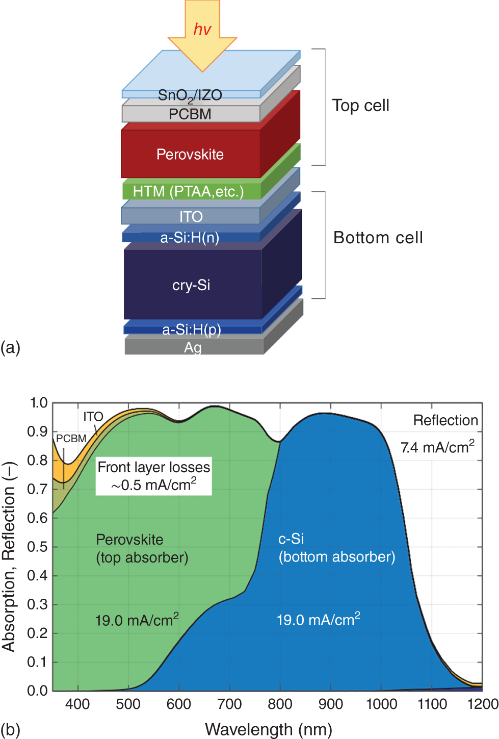
Figure 2.13 Layered structure of the stack of perovskite top cell and Si bottom cell in a 2‐terminal tandem solar cell (a), and spectral light absorption performances and corresponding photocurrent densities of top and bottom cells (b).
Source: Modified from Jäger et al. [141].
When a perovskite absorber of Cs0.17FA0.83Pb(Br0.17I0.83)3 (bandgap of 1.63 eV) was employed with the junction of an Si cell, this 2‐terminal tandem cell achieved a PCE of 23.6% with a VOC of 1.65 V [140]. Duong et al. reported a PCE of 26.4% using a 4‐terminal tandem cell with a mechanical stack of Rb‐containing quadruple cation perovskite (PCE of 17.4% with a bandgap of 1.73 eV) and silicon cells (PCE of 23.9%) [142]. What rendered the PCE higher than the above 2‐terminal cell was the higher PCE of the Si cell and the VOC gain, which was 1.81 V (1.12 V for the top, 0.69 V for the bottom). In addition to the challenges of these studies, a venture company, Oxford PV, recently reported a certified PCE of 27.3% with a perovskite and crystalline Si tandem cell (active area was 1 cm2). The PCE value achieved exceeds the top PCE of a single‐junction Si cell (26.1%). Perovskite–perovskite (all‐perovskite) type tandem cells have also been studied intensively because of their low‐cost advantage. Huang et al. fabricated an all‐perovskite tandem cell based on a simplified structure using SnO2−x and fullerene (C60) as carrier transport layers. Achieving PCE of 24.4%, the tandem cells could attain high stability, keeping efficiency almost unchanged for continuous 1‐sun illumination for 1000 hours [143].
2.9 Conclusion and Perspectives
Research of perovskite‐based photovoltaics is highly interdisciplinary. Material synthesis is mostly a solution‐based chemical process, while the characterization of perovskite semiconductors requires physical methods and device fabrication involves chemistry, physics, and electronics. Progress of the research in terms of efficiency and stability enhancement depends not only on the development of new materials but also efficient collaboration between different disciplines. A high level of defect tolerance endowed to the perovskite materials, as reflected by the long lifetimes of photoexcited free carriers, plays a central role in realizing high efficiency of devices owing to generation high voltage, which becomes especially advantageous when the perovskite device is used as an indoor power source in IoT applications where IoT devices and their secondary batteries (Li‐ion batteries, etc.) require higher voltage input under weak light to drive the circuitry. One of the goals of perovskite photovoltaics is to achieve the excellent photophysical properties of GaAs semiconductors, which exhibit an open‐circuit voltage and PCE close to the SQ limits with a bandgap of 1.42 eV at the absorption edge of nearby 900 nm, which is the optimum wavelength for a single‐junction cell to harvest the power of solar irradiation. Based on the top efficiency of PSCs (25.5%), the efficiency of perovskite modules for practical use is expected to reach more than 22%, which is considered sufficient for commercial devices in terms of cost performance. Besides R&Ds for high stability and durability of the module, ensuring environmental safety of materials is a major issue in industrialization. In the future, lead will be the subject of total replacement with other metals such as Sn, Bi, Sb, Ag, etc. If we look at applications other than photovoltaics, many applications including LED, photodetectors, and lasers are progressing and halide perovskite science and engineering is expected to continue to develop significantly in the future. For comprehensive study on the fundamentals and current advanced applications of perovskite‐based photovoltaics and optoelectronics, readers are encouraged to refer to the latest book, entitled Perovskite Photovoltaics and Optoelectronics – Fundamentals to Advanced Applications published by Wiley, as a textbook that covers the entire technology of halide perovskites [144].
References
- 1 Kojima, A., Teshima, K., Shirai, Y., and Miyasaka, T. (2009). Organometal halide perovskites as visible‐light sensitizers for photovoltaic cells. J. Am. Chem. Soc. 131: 6050–6051.
- 2 National Renewable Energy Laboratory (2020). Research cell record efficiency chart. Best research‐cell efficiencies. https://www.nrel.gov/pv/assets/pdfs/best-research-cell-efficiencies.20190802.pdf.
- 3 Jena, A.K., Kulkarni, A., and Miyasaka, T. (2019). Halide perovskite photovoltaics: background, status, and future prospects. Chem. Rev. 119: 3036–3103.
- 4 Tao, S.X., Cao, X., and Bobbert, P.A. (2017). Accurate and efficient band gap predictions of metal halide perovskites using DFT‐1/2 methods: GW accuracy with DFT expense. Sci. Rep. 7: 14386.
- 5 Tubbs, M.R. and Forty, A.J. (1964). Photographic applications of lead iodide. Br. J. Appl. Phys. 15: 1553–1558.
- 6 Kojima, A., Teshima, K., Shirai, Y., and Miyasaka, T. (2007). Novel photoelectrochemical cell with mesoscopic electrodes sensitized by lead‐halide compounds (5). The Electrochemical Society (ECS), 210th Meeting Abstracts, MA2007‐2, 352.
- 7 Lee, M.M., Teuscher, J., Miyasaka, T. et al. (2012). Efficient hybrid solar cells based on meso‐superstructured organometal halide perovskites. Science 338: 643–647.
- 8 Kojima, A., Ikegami, M., Teshima, K., and Miyasaka, T. (2012). Highly luminescent lead bromide perovskite nanoparticles synthesized with porous alumina media. Chem. Lett. 41: 397–399.
- 9 Rose, G. (1839). Beschreibung einiger neuen Mineralien des Urals. Annalen der Physik und Chemie 124: 551–573.
- 10 Chakhmouradian, A.R. and Woodward, P.M. (2014). Celebrating 175 years of perovskite research: a tribute to Roger H. Mitchell. Phys. Chem. Miner. 41: 387–391.
- 11 Katz, E.A. (2020). Perovskite: name puzzle and German–Russian odyssey of discovery. Helv. Chim. Acta 103: e2000061.
- 12 Acosta, M., Novak, N., Rojas, V. et al. (2017). BaTiO3‐based piezoelectrics: fundamentals, current status, and perspectives. Appl. Phys. Rev. 4: 041305.
- 13 Wells, H.L. (1893). Über die cäsium‐ und kalium‐bleihalogenide. Z. Anorg. Chem. 3: 195–210.
- 14 Møller, C.K. (1957). A phase transition in cæsium plumbochloride. Nature 180: 981–982.
- 15 Møller, C.K. (1957). Crystal structure and photoconductivity of cæsium plumbohalides. Nature 182: 1436.
- 16 Weber, D. (1978). CH3NH3PbX3, ein Pb(II)‐system mit kubischer perowskitstruktur/CH3NH3PbX3, a Pb(II)‐system with cubic perovskite structure. Zeitschrift für Naturforschung B 33: 1443–1445.
- 17 Weber, D. (1978). CH3NH3SnBrxI3−x (x = 0–3), ein Sn(II)‐system mit kubischer perowskitstruktur/CH3NH3SnBrxI3−x(x = 0–3), a Sn(II)‐system with cubic perovskite structure. Z. Naturforsch., B 33: 862–865.
- 18 Mitzi, D.B. (1999). Synthesis, structure, and properties of organic‐inorganic perovskites and related materials. Prog. Inorg. Chem. 48: 1–122.
- 19 Mitzi, D.B. (2000). Organic−inorganic perovskites containing trivalent metal halide layers: the templating influence of the organic cation layer. Inorg. Chem. 39: 6107–6113.
- 20 Mitzi, D.B., Wang, S., Feild, C.A. et al. (1995). Conducting layered organic‐inorganic halides containing 〈110〉‐oriented perovskite sheets. Science 267: 1473.
- 21 Era, M. and Oka, S. (2000). PbBr‐based layered perovskite film using the Langmuir–Blodgett technique. Thin Solid Films 376: 232–235.
- 22 Takeoka, Y., Asai, K., Rikukawa, M., and Sanui, K. (2001). Incorporation of conjugated polydiacetylene systems into organic–inorganic quantum‐well structures. Chem. Commun. (24): 2592–2593.
- 23 Kondo, T., Iwamoto, S., Hayase, S. et al. (1998). Resonant third‐order optical nonlinearity in the layered perovskite‐type material (C6H13NH3)2PbI4. Solid State Commun. 105: 503–506.
- 24 Tanaka, K. and Kondo, T. (2003). Bandgap and exciton binding energies in lead‐iodide‐based natural quantum‐well crystals. Sci. Technol. Adv. Mater. 4: 599–604.
- 25 Ema, K., Umeda, K., Toda, M. et al. (2006). Huge exchange energy and fine structure of excitons in an organic‐inorganic quantum well material. Phys. Rev. B 73: 241310‐1‐4.
- 26 Ishi, J., Mizuno, M., Kunugita, H. et al. (1998). Third‐order optical nonlinearity due to excitons and biexcitons in a self‐organized quantum‐well material (C6H13NH3)2PbI4. J. Nonlinear Opt. Phys. Mater. 07: 153–159.
- 27 Miyasaka, T., Ikegami, M., and Kijitori, Y. (2007). Photovoltaic performance of plastic dye‐sensitized electrodes prepared by low‐temperature binder‐free coating of mesoscopic titania. J. Electrochem. Soc. 154: A455–A461.
- 28 Miyasaka, T. (2011). Toward printable sensitized mesoscopic solar cells: light‐harvesting management with thin TiO2 films. J. Phys. Chem. Lett. 2: 262–269.
- 29 Kojima, A., Teshima, K., Shirai, Y., and Miyasaka, T. (2008). Novel photoelectrochemical cell with mesoscopic electrodes sensitized by lead‐halide compounds (11). The Electrochemical Society (ECS), 214th Meeting (PRiME. 2008), Abstracts, MA2008‐2, 27. A.
- 30 Miyasaka, T. (2015). Perovskite photovoltaics: rare functions of organo lead halide in solar cells and optoelectronic devices. Chem. Lett. 44: 720–729.
- 31 Im, J.H., Lee, C.R., Lee, J.W. et al. (2011). 6.5% efficient perovskite quantum‐dot‐sensitized solar cell. Nanoscale 3: 4088–4093.
- 32 Snaith, H.J., Petrozza, A., Ito, S. et al. (2009). Charge generation and photovoltaic operation of solid‐state dye‐sensitized solar cells incorporating a high extinction coefficient indolene‐based sensitizer. Adv. Funct. Mater. 19: 1810–1818.
- 33 Stranks, S.D., Eperon, G.E., Grancini, G. et al. (2013). Electron–hole diffusion lengths exceeding 1 micrometer in an organometal trihalide perovskite absorber. Science 342: 341–342.
- 34 Dong, Q., Fang, Y., Shao, Y. et al. (2015). Electron–hole diffusion lengths >175 μm in solution‐grown CH3NH3PbI3 single crystals. Science 347: 967–969.
- 35 Jeong, M., Choi, I.W., Go, E.M. et al. (2020). Stable perovskite solar cells with efficiency exceeding 24.8% and 0.3‐V voltage loss. Science 369: 1615–1620.
- 36 Kim, G., Min, H., Lee, K.S. et al. (2020). Impact of strain relaxation on performance of α‐formamidinium lead iodide perovskite solar cells. Science 370: 108–112.
- 37 Suarez, B., Gonzalez‐Pedro, V., Ripolles, T.S. et al. (2014). Recombination study of combined halides (Cl, Br, I) perovskite solar cells. J. Phys. Chem. Lett. 5: 1628–1635.
- 38 Eperon, G.E., Stranks, S.D., Menelaou, C. et al. (2014). Formamidinium lead trihalide: a broadly tunable perovskite for efficient planar heterojunction solar cells. Energy Environ. Sci. 7: 982–988.
- 39 Miyano, K., Tripathi, N., Yanagida, M., and Shirai, Y. (2016). Lead halide perovskite photovoltaic as a model p‐i‐n diode. Acc. Chem. Res. 49: 303–310.
- 40 Brivio, F., Butler, K.T., Walsh, A., and Schilfgaarde, M. (2014). Relativistic quasiparticle self‐consistent electronic structure of hybrid halide perovskite photovoltaic absorbers. Phys. Rev. B 89: 155204.
- 41 Tanaka, K., Takahashi, T., Ban, T. et al. (2003). Comparative study on the excitons in lead‐halide‐based perovskite‐type crystals CH3NH3PbBr3 CH3NH3PbI3. Solid State Commun. 127: 619–623.
- 42 Yin, W.J., Shi, T., and Yan, Y. (2015). Superior photovoltaic properties of lead halide perovskites: insights from first‐principles theory. J. Phys. Chem. C 119: 5253–5264.
- 43 Green, M.A., Ho‐Baillie, A., and Snaith, H.J. (2014). The emergence of perovskite solar cells. Nat. Photonics 8: 506–514.
- 44 Giorgi, G., Fujisawa, J.I., Segawa, H., and Yamashita, K. (2013). Small photocarrier effective masses featuring ambipolar transport in methylammonium lead iodide perovskite: a density functional analysis. J. Phys. Chem. Lett. 4: 4213–4216.
- 45 De Quilettes, D.W., Vorpahl, S.M., Stranks, S.D. et al. (2015). Impact of microstructure on local carrier lifetime in perovskite solar cells. Science 348: 683–686.
- 46 Stranks, S.D. and Snaith, H.J. (2015). Metal‐halide perovskites for photovoltaic and light‐emitting devices. Nat. Nanotechnol. 10: 391–402.
- 47 Miyasaka, T. (2018). Lead halide perovskites in thin film photovoltaics: background and perspectives. Bull. Chem. Soc. Jpn. 91: 1058–1068.
- 48 Liu, Z., Krückemeier, L., Krogmeier, B. et al. (2019). Open‐circuit voltages exceeding 1.26 V in planar methylammonium lead iodide perovskite solar cells. ACS Energy Lett. 4: 110–117.
- 49 Shockley, W. and Queisser, H.J. (1961). Detailed balance limit of efficiency of p–n junction solar cells. J. Appl. Phys. 32: 510–519.
- 50 Sha, W.E.I., Ren, X., Chen, L., and Choy, W.C.H. (2015). The efficiency limit of CH3NH3PbI3 perovskite solar cells. Appl. Phys. Lett. 106: 221104.
- 51 Kim, G.M., Ishii, A., Öz, S., and Miyasaka, T. (2019). MACl‐assisted Ge doping of Pb‐hybrid perovskite: a universal route to stabilize high performance perovskite solar cells. Adv. Energy Mater. 10: 1903299.
- 52 Tress, W., Marinova, N., Inganäs, O. et al. (2014). Predicting the open‐circuit voltage of CH3NH3PbI3 perovskite solar cells using electroluminescence and photovoltaic quantum efficiency spectra: the role of radiative and non‐radiative recombination. Adv. Energy Mater. 5: 1400812.
- 53 Tvingstedt, K., Malinkiewicz, O., Baumann, A. et al. (2014). Radiative efficiency of lead iodide based perovskite solar cells. Sci. Rep. 4: 6071.
- 54 Correa Baena, J.P., Steier, L., Tress, W. et al. (2015). Highly efficient planar perovskite solar cells through band alignment engineering. Energy Environ. Sci. 8: 2928–2934.
- 55 Turren‐Cruz, S.H., Hagfeldt, A., and Saliba, M. (2018). Methylammonium‐free, high‐performance, and stable perovskite solar cells on a planar architecture. Science 362: 449–453.
- 56 Smecca, E., Numata, Y., Deretzis, I. et al. (2016). Stability of solution‐processed MAPbI3 and FAPbI3 layers. Phys. Chem. Chem. Phys. 18: 13413–13422.
- 57 Miyasaka, T., Kulkarni, A., Kim, G.M. et al. (2019). Perovskite solar cells: can we go organic‐free, lead‐free, and dopant‐free? Adv. Energy Mater. 10: 1902500.
- 58 Ono, L.K., Juarez‐Perez, E.J., and Qi, Y. (2017). Progress on perovskite materials and solar cells with mixed cations and halide anions. ACS Appl. Mater. Interfaces 9: 30197–30246.
- 59 Akin, S., Akman, E., and Sonmezoglu, S. (2020). FAPbI3‐based perovskite solar cells employing hexyl‐based ionic liquid with an efficiency over 20% and excellent long‐term stability. Adv. Funct. Mater. 30: 2002964.
- 60 Jeon, N.J., Noh, J.H., Yang, W.S. et al. (2015). Compositional engineering of perovskite materials for high‐performance solar cells. Nature 517: 476–480.
- 61 Niu, G., Li, W., Li, J. et al. (2017). Enhancement of thermal stability for perovskite solar cells through cesium doping. RSC Adv. 7: 17473–17479.
- 62 Li, Z., Yang, M., Park, J.S. et al. (2016). Stabilizing perovskite structures by tuning tolerance factor: formation of formamidinium and cesium lead iodide solid‐state alloys. Chem. Mater. 28: 284–292.
- 63 Zhang, Y., Liu, M., Eperon, G.E. et al. (2015). Charge selective contacts, mobile ions and anomalous hysteresis in organic–inorganic perovskite solar cells. Mater. Horiz. 2: 315–322.
- 64 Ravishankar, S., Almora, O., Echeverría‐Arrondo, C. et al. (2017). Surface polarization model for the dynamic hysteresis of perovskite solar cells. J. Phys. Chem. Lett. 8: 915–921.
- 65 Weber, S.A.L., Hermes, I.M., Turren‐Cruz, S.H. et al. (2018). How the formation of interfacial charge causes hysteresis in perovskite solar cells. Energy Environ. Sci. 11: 2404–2413.
- 66 Almosni, S., Cojocaru, L., Li, D. et al. (2017). Tunneling‐assisted trapping as one of the possible mechanisms for the origin of hysteresis in perovskite solar cells. Energy Technol. 5: 1767–1774.
- 67 Singh, T. and Miyasaka, T. (2017). Stabilizing the efficiency beyond 20% with a mixed cation perovskite solar cell fabricated in ambient air under controlled humidity. Adv. Energy Mater. 8: 1700677. (1–9).
- 68 Saliba, M., Matsui, T., Domanski, K. et al. (2016). Incorporation of rubidium cations into perovskite solar cells improves photovoltaic performance. Science 354: 206–209.
- 69 Hu, Y., Hutter Eline, M., Rieder, P. et al. (2018). Understanding the role of cesium and rubidium additives in perovskite solar cells: trap states, charge transport, and recombination. Adv. Energy Mater. 8: 1703057. (1–11).
- 70 Han, G., Hadi, H.D., Bruno, A. et al. (2018). Additive selection strategy for high performance perovskite photovoltaics. J. Phys. Chem. C 122: 13884–13893.
- 71 Brunetti, B., Cavallo, C., Ciccioli, A. et al. (2016). On the thermal and thermodynamic (in)stability of methylammonium lead halide perovskites. Sci. Rep. 6: 31896. (1–12).
- 72 Wang, R., Mujahid, M., Duan, Y. et al. (2019). A review of perovskites solar cell stability. Adv. Funct. Mater. 29: 1808843.
- 73 Shi, L., Bucknall, M.P., Young, T.L. et al. (2020). Gas chromatography–mass spectrometry analyses of encapsulated stable perovskite solar cells. Science 368: eaba2412.
- 74 Eames, C., Frost, J.M., Barnes, P.R.F. et al. (2015). Ionic transport in hybrid lead iodide perovskite solar cells. Nat. Commun. 6: 7497. (1–8).
- 75 Minns, J.L., Zajdel, P., Chernyshov, D. et al. (2017). Structure and interstitial iodide migration in hybrid perovskite methylammonium lead iodide. Nat. Commun. 8: 15152. (1–5).
- 76 Yuan, Y., Chae, J., Shao, Y. et al. (2015). Photovoltaic switching mechanism in lateral structure hybrid perovskite solar cells. Adv. Energy Mater. 5: 1500615. (1–7).
- 77 Leguy, A.M.A., Hu, Y., Campoy‐Quiles, M. et al. (2015). Reversible hydration of CH3NH3PbI3 in films, single crystals, and solar cells. Chem. Mater. 27: 3397–3407.
- 78 Habisreutinger, S.N., Leijtens, T., Eperon, G.E. et al. (2014). Carbon nanotube/polymer composites as a highly stable hole collection layer in perovskite solar cells. Nano Lett. 14: 5561–5568.
- 79 Chaudhary, B., Kulkarni, A., Jena, A.K. et al. (2017). Poly(4‐vinylpyridine)‐based interfacial passivation to enhance voltage and moisture stability of lead halide perovskite solar cells. ChemSusChem 10: 2473–2479.
- 80 Hou, Y., Zhou, Z.R., Wen, T. et al. (2019). Enhanced moisture stability of metal halide perovskite solar cells based on sulfur‐oleylamine surface modification. Nanoscale Horiz. 4: 208–213.
- 81 Abdelmageed, G., Sully, H.R., Bonabi Naghadeh, S. et al. (2018). Improved stability of organometal halide perovskite films and solar cells toward humidity via surface passivation with oleic acid. ACS Appl. Energy Mater. 1: 387–392.
- 82 Cao, J., Li, C., Lv, X. et al. (2018). Efficient grain boundary suture by low‐cost tetra‐ammonium zinc phthalocyanine for stable perovskite solar cells with expanded photoresponse. J. Am. Chem. Soc. 140: 11577–11580.
- 83 Grancini, G., Roldán‐Carmona, C., Zimmermann, I. et al. (2017). One‐year stable perovskite solar cells by 2D/3D interface engineering. Nat. Commun. 8: 15684.
- 84 Lu, J., Jiang, L., Li, W. et al. (2017). Diammonium and monoammonium mixed‐organic‐cation perovskites for high performance solar cells with improved stability. Adv. Energy Mater. 7: 1700444. (1–10).
- 85 Chen, P., Bai, Y., Wang, S. et al. (2018). In situ growth of 2D perovskite capping layer for stable and efficient perovskite solar cells. Adv. Funct. Mater. 28: 1706923.
- 86 Ye, J., Zheng, H., Zhu, L. et al. (2017). Enhanced moisture stability of perovskite solar cells with mixed‐dimensional and mixed‐compositional light‐absorbing materials. Solar RRL 1: 1700125. (1–8).
- 87 Xu, H., Sun, Y., Zheng, H. et al. (2019). High‐performance and moisture‐stable perovskite solar cells with a 2D modified layer via introducing a high dipole moment cation. J. Mater. Chem. C 7: 15276–15284.
- 88 Safdari, M., Svensson, P.H., Hoang, M.T. et al. (2016). Layered 2D alkyldiammonium lead iodide perovskites: synthesis, characterization, and use in solar cells. J. Mater. Chem. A 4: 15638–15646.
- 89 Chen, M., Li, P., Liang, C. et al. (2020). Enhanced efficiency and stability of perovskite solar cells by 2D perovskite vapor‐assisted interface optimization. J. Energy Chem. 45: 103–109.
- 90 Mei, A., Li, X., Liu, L. et al. (2014). A hole‐conductor–free, fully printable mesoscopic perovskite solar cell with high stability. Science 345: 295–298.
- 91 Grancini, G., Roldán‐Carmona, C., Zimmermann, I. et al. (2017). One‐year stable perovskite solar cells by 2D/3D. Nat. Commun. 8: 15684.
- 92 Fagiolari, L. and Bella, F. (2019). Carbon‐based materials for stable, cheaper and large‐scale processable perovskite solar cells. Energy Environ. Sci. 12: 3437–3472.
- 93 Yavari, M., Mazloum‐Ardakani, M., Gholipour, S. et al. (2018). Reducing surface recombination by a poly(4‐vinylpyridine) interlayer in perovskite solar cells with high open‐circuit voltage and efficiency. ACS Omega 3: 5038–5043.
- 94 Zong, Y., Zhou, Y., Zhang, Y. et al. (2018). Continuous grain‐boundary functionalization for high‐efficiency perovskite solar cells with exceptional stability. Chemistry 4: 1404–1415.
- 95 Lee, S.W., Kim, S., Bae, S. et al. (2016). UV degradation and recovery of perovskite solar cells. Sci. Rep. 6: 38150. (1‐10).
- 96 Luo, Y., Khoram, P., Brittman, S. et al. (2017). Direct observation of halide migration and its effect on the photoluminescence of methylammonium lead bromide perovskite single crystals. Adv. Mater. 29: 1703451. (1–7).
- 97 Nie, W., Blancon, J.C., Neukirch, A.J. et al. (2016). Light‐activated photocurrent degradation and self‐healing in perovskite solar cells. Nat. Commun. 7: 11574. (1–9).
- 98 Bischak, C.G., Hetherington, C.L., Wu, H. et al. (2017). Origin of reversible photoinduced phase separation in hybrid perovskites. Nano Lett. 17: 1028–1033.
- 99 Hoke, E.T., Slotcavage, D.J., Dohner, E.R. et al. (2015). Reversible photo‐induced trap formation in mixed‐halide hybrid perovskites for photovoltaics. Chem. Sci. 6: 613–617.
- 100 Yun Jae, S., Seidel, J., Kim, J. et al. (2016). Critical role of grain boundaries for ion migration in formamidinium and methylammonium lead halide perovskite solar cells. Adv. Energy Mater. 6: 1600330. (1–8).
- 101 Jena, A.K., Numata, Y., Ikegami, M., and Miyasaka, T. (2018). Role of spiro‐OMeTAD in performance deterioration of perovskite solar cells at high temperature and reuse of the perovskite films to avoid Pb‐waste. J. Mater. Chem. A 6: 2219–2230.
- 102 Jena, A.K., Ikegami, M., and Miyasaka, T. (2017). Severe morphological deformation of spiro‐OMeTAD in (CH3NH3)PbI3 solar cells at high temperature. ACS Energy Lett. 2: 1760–1761.
- 103 Carrillo, J., Guerrero, A., Rahimnejad, S. et al. (2016). Ionic reactivity at contacts and aging of methylammonium lead triiodide perovskite solar cells. Adv. Energy Mater. 6: 1502246. (1–7).
- 104 Zhao, Y., Zhou, W., Tan, H. et al. (2017). Mobile‐ion‐induced degradation of organic hole‐selective layers in perovskite solar cells. J. Phys. Chem. C 121: 14517–14523.
- 105 Rakstys, K., Igci, C., and Nazeeruddin, M.K. (2019). Efficiency vs. stability: dopant‐free hole transporting materials towards stabilized perovskite solar cells. Chem. Sci. 10: 6748–6769.
- 106 Yang, W.S., Park, B.W., Jung, E.H. et al. (2017). Iodide management in formamidinium‐lead‐halide–based perovskite layers for efficient solar cells. Science 356: 1376–1379.
- 107 Huang, C., Fu, W., Li, C.Z. et al. (2016). Dopant‐free hole‐transporting material with a C3h symmetrical truxene core for highly efficient perovskite solar cells. J. Am. Chem. Soc. 138: 2528–2531.
- 108 Cao, Y., Li, Y., Morrissey, T. et al. (2019). Dopant‐free molecular hole transport material that mediates a 20% power conversion efficiency in a perovskite solar cell. Energy Environ. Sci. 12: 3502–3507.
- 109 Paek, S., Qin, P., Lee, Y. et al. (2017). Dopant‐free hole‐transporting materials for stable and efficient perovskite solar cells. Adv. Mater. 29: 1606555.
- 110 Feng, Y., Hu, Q., Rezaee, E. et al. (2019). Perovskite solar cells: high performance and stable perovskite solar cells based on dopant‐free arylamine‐substituted copper(II) phthalocyanine hole‐transporting materials. Adv. Energy Mater. 9: 1970104.
- 111 Zhang, L., Liu, C., Zhang, J. et al. (2018). Intensive exposure of functional rings of a polymeric hole‐transporting material enables efficient perovskite solar cells. Adv. Mater. 30: 1804028.
- 112 Kim, G.‐W., Lee, J., Kang, G. et al. (2018). Donor–acceptor type dopant‐free, polymeric hole transport material for planar perovskite solar cells (19.8%). Adv. Energy Mater. 8: 1701935.
- 113 Öz, S., Jena, A., Kulkarni, A. et al. (2020). Lead(II) propionate additive and a dopant‐free polymer hole transport material for CsPbI2Br perovskite solar cells. ACS Energy Lett. 5: 1292–1299.
- 114 Guo, Z., Jena, A.K., Takei, I. et al. (2020). VOC over 1.4 V for amorphous tin oxide‐based dopant‐free CsPbI2Br perovskite solar cells. J. Am. Chem. Soc. 142: 9725–9734.
- 115 Eperon, G.E., Paterno, G.M., Sutton, R.J. et al. (2015). Inorganic caesium lead iodide perovskite solar cells. J. Mater. Chem. A 3: 19688–19695.
- 116 Wang, Y., Dar, M.I., Ono, L.K. et al. (2019). Thermodynamically stabilized β‐CsPbI3–based perovskite solar cells with efficiencies >18%. Science 365: 591–595.
- 117 Zhang, T., Dar, M.I., Li, G. et al. (2017). Bication lead iodide 2D perovskite component to stabilize inorganic α‐CsPbI3 perovskite phase for high‐efficiency solar cells. Sci. Adv. 3: e1700841. (1–7).
- 118 Jena, A.K., Kulkarni, A., Sanehira, Y. et al. (2018). Stabilization of α‐CsPbI3 in ambient room temperature conditions by incorporating Eu into CsPbI3. Chem. Mater. 30: 6668–6674.
- 119 Babayigit, A., Ethirajan, A., Muller, M., and Conings, B. (2016). Toxicity of organometal halide perovskite solar cells. Nat. Mater. 15: 247–251.
- 120 Ke, W. and Kanatzidis, M.G. (2019). Prospects for low‐toxicity lead‐free perovskite solar cells. Nat. Commun. 10: 965.
- 121 Jokar, E., Chien, C.H., Tsai, C.M. et al. (2019). Robust tin‐based perovskite solar cells with hybrid organic cations to attain efficiency approaching 10%. Adv. Mater. 31: 1804835.
- 122 Liu, X., Wang, Y., Wu, T. et al. (2020). Efficient and stable tin perovskite solar cells enabled by amorphous‐polycrystalline structure. Nat. Commun. 11: 2678.
- 123 Tai, Q., Guo, X., Tang, G. et al. (2019). Antioxidant grain passivation for air‐stable tin‐based perovskite solar cells. Angew. Chem. 58: 806–810.
- 124 Kamarudin, M.A., Hirotani, D., Wang, Z. et al. (2019). Suppression of charge carrier recombination in lead‐free tin halide perovskite via Lewis base post‐treatment. J. Phys. Chem. Lett. 10 (17): 5277–5283.
- 125 Kawai, T., Ishii, A., Kitamura, T. et al. (1996). Optical absorption in band‐edge region of (CH3NH3)3Bi2I9 single crystals. J. Phys. Soc. Jpn. 65: 1464–1468.
- 126 Arakcheeva, A., Bonin, M., Chapuis, G., and Zaitsev, A.I. (1999). The phases of Cs3Bi2I9 between RT and 190 K. Z. Kristallogr. ‐ Cryst. Mater. 214: 279–283.
- 127 Szklarz, P., Pietraszko, A., Jakubas, R. et al. (2008). Structure, phase transitions and molecular dynamics of [C(NH2)3]3[M2I9], M = Sb, Bi. J. Phys. Condens. Matter 20: 255221.
- 128 Kulkarni, A., Singh, T., Ikegami, M., and Miyasaka, T. (2017). Photovoltaic enhancement of bismuth halide hybrid perovskite by N‐methyl pyrrolidone‐assisted morphology conversion. RSC Adv. 7: 9456–9460.
- 129 Jain, S.M., Phuyal, D., Davies, M.L. et al. (2018). An effective approach of vapour assisted morphological tailoring for reducing metal defect sites in lead‐free, (CH3NH3)3Bi2I9 bismuth‐based perovskite solar cells for improved performance and long‐term stability. Nano Energy 49: 614–624.
- 130 Kulkarni, A., Jena, A.K., Ikegami, M., and Miyasaka, T. (2019). Performance enhancement of AgBi2I7 solar cells by modulating a solvent‐mediated adduct and tuning remnant BiI3 in one‐step crystallization. Chem. Commun. 55: 4031–4034.
- 131 Kim, H.D., Ohkita, H., Benten, H., and Ito, S. (2016). Photovoltaic performance of perovskite solar cells with different grain sizes. Adv. Mater. 28: 917–922.
- 132 Boopathi, K.M., Karuppuswamy, P., Singh, A. et al. (2017). Solution‐processable antimony‐based light‐absorbing materials beyond lead halide perovskites. J. Mater. Chem. A 5: 20843–20850.
- 133 Jiang, F., Yang, D., Jiang, Y. et al. (2018). Chlorine‐incorporation‐induced formation of the layered phase for antimony‐based lead‐free perovskite solar cells. J. Am. Chem. Soc. 140: 1019–1027.
- 134 Nie, R., Mehta, A., Park, B.W. et al. (2018). Mixed sulfur and iodide‐based lead‐free perovskite solar cells. J. Am. Chem. Soc. 140: 872–875.
- 135 Chen, M., Ju, M.G., Carl, A.D. et al. (2018). Cesium titanium(IV) bromide thin films based stable lead‐free perovskite solar cells. Joule 2: 558–570.
- 136 Nie, R., Sumukam, R.R., Reddy, S.H. et al. (2020). Lead‐free perovskite solar cells enabled by hetero‐valent substitutes. Energy Environ. Sci. 13: 2363–2385.
- 137 Jošt, M., Kegelmann, L., Korte, L., and Albrecht, S. (2020). Monolithic perovskite tandem solar cells: a review of the present status and advanced characterization methods toward 30% efficiency. Adv. Energy Mater. 10: 1904102.
- 138 Zhang, A., Li, Z., Meng, L. et al. (2020). Perovskite‐based tandem solar cells: get the most out of the sun. Adv. Funct. Mater. 30: 2001904.
- 139 McMeekin, D.P., Sadoughi, G., Rehman, W. et al. (2016). A mixed‐cation lead mixed‐halide perovskite absorber for tandem solar cells. Science 351: 151–155.
- 140 Bush, K.A., Palmstrom, A.F., Yu, Z.J. et al. (2017). 23.6%‐efficient monolithic perovskite/silicon tandem solar cells with improved stability. Nat. Energy 2: 17009.
- 141 Jäger, K., Kolte, L., Rech, B., and Albrecht, S. (2017). Numerical optical optimization of monolithic planar perovskite‐silicon tandem solar cells with regular and inverted device architectures. Opt. Express 25: A473–A482.
- 142 Duong, T., Wu, Y., Shen, H. et al. (2017). Rubidium multication perovskite with optimized bandgap for perovskite‐silicon tandem with over 26% efficiency. Adv. Energy Mater. 7: 1700228.
- 143 Yu, Z., Yang, Z., Ni, Z. et al. (2020). Simplified interconnection structure based on C60/SnO2−x for all‐perovskite tandem solar cells. Nat. Energy 5: 657–665.
- 144 Miyasaka, T. (2021). Perovskite Photovoltaics and Optoelectronics – Fundamentals to Advanced Applications. Wiley.