
Appendices
Appendix A
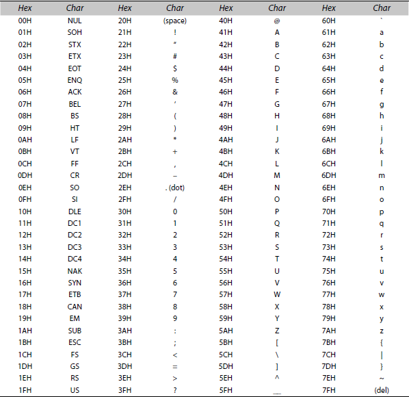
A.1 ASCII Codes for the Characters (Char)
Assume msb b7 (parity bit) = 0
Appendix B
B.1 8051 Internal and External RAM Byte Addresses between 00H to FFH and RAM bit Addresses of 7th, 6th, 5th, 4th, 3rd, 2nd, 1st and 0th bit
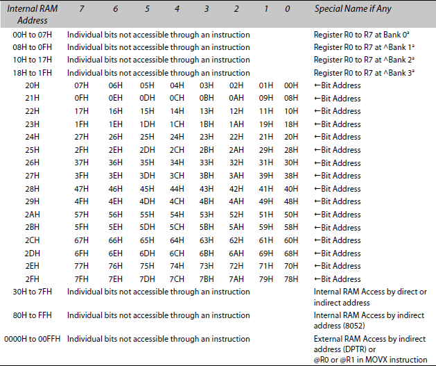
a Bank is 0 or 1 or 2 or 3 as per pre-defined bits at RS0 and RSI in PSW.
Appendix C
C.1 Addresses of SFR bytes and Addresses and Names of their each bit from 0th to 7th
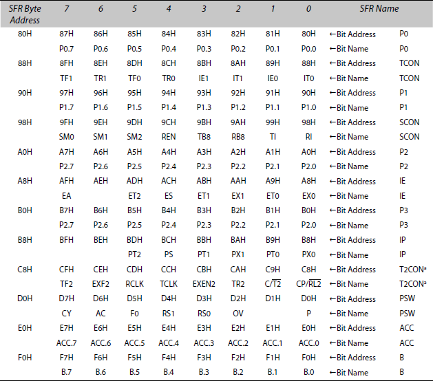
a 8052
Appendix D
D.1 SFR with Byte Addresses (when SFR bits have no individual bit addresses)
| SFR Byte Address ↙ | SFR Abbreviation and Name | |
|---|---|---|
99H |
SBUF |
Serial Port SI interface buffer |
87H |
PCON |
Power Control |
81H |
SP |
Stack Pointer |
82H |
DPL |
Data pointer Lower Byte |
83H |
DPH |
Data pointer Upper Byte |
89H |
TMOD |
Timer/Counter Mode Control |
8CH |
TH0 |
Timer/Counter 0 Upper Byte |
8AH |
TL0 |
Timer/Counter 0 Lower Byte |
8DH |
TH1 |
Timer/Counter 1 Upper Byte |
8BH |
TL1 |
Timer/Counter 1 Lower Byte |
0CDH |
TH2 |
Timer/Counter 2 Upper Byte 8052 |
0CCH |
TL2 |
Timer/Counter 2 Lower Byte 8052 |
0CBH |
RCAP2H |
Reload/Capture Register Timer 2 Upper Byte 8052 |
0CAH |
RCAP2L |
Reload/Capture Register Timer 2 Lower Byte 8052 |
Appendix E
E.1 SFR Bits Default values (Bits on processor reset on power-up or timeout reset from watchdog timer)
Bits on processor reset on power-up or timeout reset from watchdog timer are as follows:
X means can be any, 0 or 1.
| SFR Byte Address ↙ | SFR Name | Default Bitsa |
|---|---|---|
99H |
SBUF |
Indeterminate |
87H |
PCON (HCMOS) |
0XXXXXXX |
|
PCON (CHMOS) |
0XXX0000 |
81H |
SP |
00000111 |
82H |
DPL |
00000000 |
83H |
DPH |
00000000 |
89H |
TMOD |
00000000 |
8CH |
TH0 |
00000000 |
8AH |
TL0 |
00000000 |
8DH |
TH1 |
00000000 |
8BH |
TL1 |
00000000 |
CDH |
TH2 |
00000000 (8052) |
CCH |
TL2 |
00000000 (8052) |
CBH |
RCAP2H |
00000000 (8052) |
CAH |
RCAP2L |
00000000 (8052) |
F0H |
B |
00000000 |
E0H |
A |
00000000 |
D0H |
PSW |
00000000 |
C8H |
T2CON (8052) |
00000000 |
B8H |
IP (8051) |
XXX00000 |
B8H |
IP (8052) |
XX000000 |
B0H |
P3 |
11111111 |
A0H |
P2 |
11111111 |
90H |
P1 |
11111111 |
80H |
P0 |
11111111 |
A8H |
IE |
(8051) 0XX00000 |
A8H |
IE |
(8052) 0X000000 |
98H |
SCON |
00000000 |
88H |
TCON |
00000000 |
Appendix F
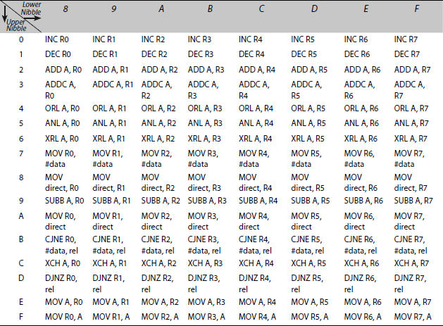
F.1 8051-Opcodes to Instruction Mnemonics Conversion Table

Note: /bit means complement of bit at the bit address.
Appendix G
G.1 8051 Instruction Mnemonics along with the opcode
| Opcode (Hex) | Instruction Mnemonics |
|---|---|
Arithmetic ADD, DA,CLR, MUL and DIV Instructions |
|
24 |
ADD A, #data |
25 |
ADD A, direct |
26 |
ADD A, @R0 |
27 |
ADD A, @R1 |
28 |
ADD A, R0 |
29 |
ADD A, R1 |
2A |
ADD A, R2 |
2B |
ADD A, R3 |
2C |
ADD A, R4 |
2D |
ADD A, R5 |
2E |
ADD A, R6 |
2F |
ADD A, R7 |
34 |
ADDC A, #data |
35 |
ADDC A, direct |
36 |
ADDC A, @R0 |
37 |
ADDC A, @R1 |
38 |
ADDC A, R0 |
39 |
ADDC A, R1 |
3A |
ADDC A, R2 |
3B |
ADDC A, R3 |
3C |
ADDC A, R4 |
3D |
ADDC A, R5 |
3E |
ADDC A, R6 |
3F |
ADDC A, R7 |
D4 |
DA A |
A4 |
MUL AB |
84 |
DIV AB |
E4 |
CLR A |
Decrement Instructions |
|
14 |
DEC A |
15 |
DEC direct |
16 |
DEC@R0 |
17 |
DEC@R1 |
18 |
DEC R0 |
19 |
DEC R1 |
1A |
DEC R2 |
1B |
DEC R3 |
1C |
DEC R4 |
1D |
DEC R5 |
1E |
DEC R6 |
1F |
DEC R7 |
04 |
INC A |
05 |
INC direct |
06 |
INC @R0 |
07 |
INC @R1 |
08 |
INC R0 |
09 |
INC R1 |
0A |
INC R2 |
0B |
INC R3 |
0C |
INC R4 |
0D |
INC R5 |
0E |
INC R6 |
0F |
INC R7 |
A3 |
INC DPTR |
Logic AND-OR-NOT Instructions |
|
52 |
ANL direct, A |
53 |
ANL direct, #data |
54 |
ANL A, #data |
55 |
ANL A, direct |
56 |
ANL A, @R0 |
57 |
ANL A, @R1 |
58 |
ANL A, R0 |
59 |
ANL A, R1 |
5A |
ANL A, R2 |
5B |
ANL A, R3 |
5C |
ANL A, R4 |
5D |
ANL A, R5 |
5E |
ANL A, R6 |
5F |
ANL A, R7 |
42 |
ORL direct, A |
43 |
ORL direct, #data |
44 |
ORL A, #data |
45 |
ORL A, direct |
46 |
ORL A, @R0 |
47 |
ORL A, @R1 |
48 |
ORL A, R0 |
49 |
ORL A, R1 |
4A |
ORL A, R2 |
4B |
ORL A, R3 |
4C |
ORL A, R4 |
4D |
ORL A, R5 |
4E |
ORL A, R6 |
4F |
ORL A, R7 |
F4 |
CPL A |
Subtract Instructions |
|
94 |
SUBB A, #data |
95 |
SUBB A, direct |
96 |
SUBB A, @R0 |
97 |
SUBB A, @R1 |
98 |
SUBB A, R0 |
99 |
SUBB A, R1 |
9A |
SUBB A, R2 |
9B |
SUBB A, R3 |
9C |
SUBB A, R4 |
9D |
SUBB A, R5 |
9E |
SUBB A, R6 |
9F |
SUBB A, R7 |
62 |
XRL direct, A |
64 |
XRL A, #data |
65 |
XRL A, direct |
66 |
XRL A, @R0 |
67 |
XRL A, @R1 |
68 |
XRL A, R0 |
69 |
XRL A, R1 |
6A |
XRL A, R2 |
6B |
XRL A, R3 |
6C |
XRL A, R4 |
6D |
XRL A, R5 |
6E |
XRL A, R6 |
6F |
XRL A, R7 |
Rotate and Swap Instructions |
|
23 |
RL A |
33 |
RLC A |
03 |
RR A |
13 |
RRC A |
C4 |
SWAP A |
Return and Call Instructions |
|
^1 |
ACALL addr11 |
12 |
LCALL addr16 |
22 |
RET |
32 |
RETI |
Program Flow Control Instructions |
|
00 |
NOP |
B4 |
CJNE A, #data, rel |
B5 |
CJNE A, direct, rel |
B6 |
CJNE @R0, #data, rel |
B7 |
CJNE @R1, #data, rel |
B8 |
CJNE R0, #data, rel |
B9 |
CJNE R1, #data, rel |
BA |
CJNE R2, #data, rel |
BB |
CJNE R3, #data, rel |
BC |
CJNE R4, #data, rel |
BD |
CJNE R5, #data, rel |
BE |
CJNE R6, #data, rel |
BF |
CJNE R7, #data, rel |
D5 |
DJNZ direct, rel |
D8 |
DJNZ R0, rel |
D9 |
DJNZ R1, rel |
DA |
DJNZ R2, rel |
DB |
DJNZ R3, rel |
DC |
DJNZ R4, rel |
DD |
DJNZ R5, rel |
DE |
DJNZ R6, rel |
DF |
DJNZ R7, rel |
20 |
JB bit, rel |
40 |
JC rel |
10 |
JBC bit, rel |
30 |
JNB bit, rel |
50 |
JNC, rel |
60 |
JZ rel |
JNZ rel |
|
80 |
SJMP rel |
^1 |
AJMP addr11 |
02 |
LJMP addr16 |
73 |
JMP @A + DPTR |
Bit Manipulation and Bit Move Instructions |
|
82 |
ANL C, bit |
B0 |
ANL C, /bit |
C3 |
CLR C |
C2 |
CLR bit |
B3 |
CPL C |
B2 |
CPL bit |
A2 |
MOV C, bit |
92 |
MOV bit, C |
72 |
ORL C, bit |
A0 |
ORL C, /bit |
D3 |
SETB C |
D2 |
SETB bit |
MOV Instructions |
|
E5 |
MOV A, direct |
E6 |
MOV A, @R0 |
E7 |
MOV A, @R1 |
E8 |
MOV A, R0 |
E9 |
MOV A, R1 |
EA |
MOV A, R2 |
EB |
MOV A, R3 |
EC |
MOV A, R4 |
ED |
MOV A, R5 |
EE |
MOV A, R6 |
EF |
MOV A, R7 |
74 |
MOV A, #data |
75 |
MOV direct, #data |
76 |
MOV @R0, #data |
77 |
MOV @R1, #data |
78 |
MOV R0, #data |
79 |
MOV R1, #data |
7A |
MOV R2, #data |
7B |
MOV R3, #data |
7C |
MOV R4, #data |
7D |
MOV R5, #data |
7E |
MOV R6, #data |
7F |
MOV R7, #data |
F5 |
MOV direct, A |
F6 |
MOV @R0, A |
F7 |
MOV @R1, A |
F8 |
MOV R0, A |
F9 |
MOV R1, A |
FA |
MOV R2, A |
FB |
MOV R3, A |
FC |
MOV R4, A |
FD |
MOV R5, A |
FE |
MOV R6, A |
FF |
MOV R7, A |
A6 |
MOV @R0, direct |
A7 |
MOV @R1, direct |
A8 |
MOV R0, direct |
A9 |
MOV R1, direct |
AA |
MOV R2, direct |
AB |
MOV R3, direct |
MOV R4, direct |
|
AD |
MOV R5, direct |
AE |
MOV R6, direct |
AF |
MOV R7, direct |
85 |
MOV direct, direct |
86 |
MOV direct, @R0 |
87 |
MOV direct, @R1 |
90 |
MOV DPTR, #data16 |
93 |
MOVC A, @A + DPTR |
83 |
MOVC A, @A + PC |
88 |
MOV direct, R0 |
89 |
MOV direct, R1 |
8A |
MOV direct, R2 |
8B |
MOV direct, R3 |
8C |
MOV direct, R4 |
8D |
MOV direct, R5 |
8E |
MOV direct, R6 |
8F |
MOV direct, R7 |
E0 |
MOVX A, @DPTR |
E2 |
MOVX A, @R0 |
E3 |
MOVX A, @R1 |
F0 |
MOVX @DPTR, A |
F2 |
MOVX @R0, A |
F3 |
MOVX @R1, A |
C5 |
MOV direct, R4 |
C6 |
MOV direct, R5 |
C7 |
MOV direct, R6 |
C8 |
MOV direct, R7 |
C9 |
MOV direct, direct |
CA |
MOVX A, @DPTR |
CB |
MOVX A, @R0 |
CC |
MOVX A, @R1 |
CD |
MOVX @DPTR, A |
CE |
MOVX @R0, A |
CF |
MOVX @R1, A |
Push-Pop and Exchange lower nibble Instructions |
|
D0 |
POP direct |
C0 |
PUSH direct |
D6 |
XCHD A, @R0 |
D7 |
XCHD A, @R1 |
Note: (1) bit means address of the bit in bit operation; @Ri means indirect RAM address in R0 or R1; /bit means complement of the bit. Rn means n-th register of register bank that RS0and Rs1 specifies; #data mean 8-bit immediate operand and #data16 means16-bit immediate operand; direct means address of the byte in byte operation on SFR or internal RAM at lower 128 bytes. (2) ^ Three bits of opcode are as per remaining 3 msbs in 11-bit address. [addr11 means 11-bit address.] For example, 01H, 21H, 41H, 61H, 81H, A1H, C1H and E1H are opcodes for AJMP. Three msbs b7-b6-b5 are 000 in opcode 01H instruction. Therefore, upper3-bits of address are also 000 in that AJMP instruction. The 11H, 31H, 51H, 71H, 91H, B1H, D1H and F1H are opcodes for ACALL. Three msbs are 100 in opcode 91H instruction. Therefore, upper3-bits of address are also 100 in that AJMP instruction. The opcode lower five b4-b0 bits are 00001 in AJMP and 10001 in ACALL. (3) The rel means signed two’s complement between −128 to +127 (4) addr16 means 16-bit address.
Appendix H
H1 8051 Instruction Mnemonics, Length and Cycles for Execution
Length (L) is in bytes and number of cycles (C), 1 cycle = 1 μs (period of 12 oscillations) for 12 MHz XTAL.
| Instruction Mnemonics | L | C |
|---|---|---|
Arithmetic Instructions |
||
ADD A, #data |
2 |
1 |
ADD A, @Ri |
1 |
1 |
ADD A, Rn |
1 |
1 |
ADD A, direct |
2 |
1 |
ADDC A, #data |
2 |
1 |
ADDC A, @Ri |
1 |
1 |
ADDC A, Rn |
1 |
1 |
ADDC A, Direct |
2 |
1 |
DA A |
1 |
1 |
DEC A |
1 |
1 |
DEC @Ri |
1 |
1 |
DEC Rn |
1 |
1 |
DEC direct |
2 |
1 |
INC A |
1 |
1 |
INC @Ri |
1 |
1 |
INC Rn |
1 |
1 |
INC direct |
2 |
1 |
INC DPTR |
1 |
2 |
SUBB A, #data |
2 |
1 |
SUBB A, Rn |
1 |
1 |
SUBB A, @Ri |
1 |
1 |
SUBB A, direct |
2 |
1 |
MUL AB |
1 |
4 |
DIV AB |
1 |
4 |
CLR A |
1 |
1 |
Rotate and Swap Instructions |
||
RL A |
1 |
1 |
RLC A |
1 |
1 |
RR A |
1 |
1 |
RRC A |
1 |
1 |
SWAP A |
1 |
1 |
Logic Instructions |
||
CPL A |
1 |
1 |
ANL A, direct |
2 |
1 |
ANL A, #data |
2 |
1 |
ANL A, @Ri |
1 |
1 |
ANL A, Rn |
1 |
1 |
ANL A, direct |
2 |
1 |
ANL A, #data |
2 |
1 |
ANL direct, #data |
3 |
2 |
ANL direct, A |
2 |
1 |
ORL A, direct |
2 |
1 |
ORL direct, #data |
3 |
2 |
ORL direct, A |
2 |
1 |
ORL A, #data |
2 |
1 |
ORL A, @Ri |
1 |
1 |
ORL A, Rn |
1 |
1 |
XRL A, #data |
2 |
1 |
XRL A, @Ri |
1 |
1 |
XRL A, Rn |
1 |
1 |
XRL A, direct |
2 |
1 |
3 |
2 |
|
XRL direct, A |
2 |
1 |
Bit Manipulation and Bit Move Instructions |
||
SETB C |
1 |
1 |
CLR C |
1 |
1 |
CPL C |
1 |
1 |
SETB bit |
2 |
1 |
CLR bit |
2 |
1 |
CPL bit |
2 |
1 |
MOV C, bit |
2 |
1 |
MOV bit, C |
2 |
2 |
ORL C, bit |
2 |
2 |
ORL C, /bit |
2 |
2 |
ANL C, bit |
2 |
2 |
ANL C, /bit |
2 |
2 |
Program Flow Control Instructions |
||
NOP |
1 |
1 |
CJNE A, #data, rel |
3 |
2 |
CJNE A, direct, rel |
3 |
2 |
CJNE @Ri, #data, rel |
3 |
2 |
CJNE Rn, #data, rel |
3 |
2 |
DJNZ direct, rel |
3 |
2 |
DJNZ Rn, rel |
2 |
2 |
JB bit, rel |
3 |
2 |
JC rel |
2 |
2 |
JBC bit, rel |
2 |
2 |
JNB bit, rel |
2 |
2 |
JNC rel |
2 |
2 |
JZ rel |
2 |
2 |
JNZ rel |
2 |
2 |
SJMP rel |
2 |
2 |
LJMP addr16 |
3 |
2 |
AJMP addr11 |
2 |
2 |
ACALL addr11 |
2 |
2 |
JMP @A + DPTR |
1 |
2 |
LCALL addr16 |
3 |
2 |
RET |
1 |
2 |
RETI |
1 |
2 |
Data Move, push-pop and Exchange Instructions |
||
MOV A, #data |
2 |
1 |
MOV A, @Ri |
1 |
1 |
MOV A, Rn |
1 |
1 |
MOV A, direct |
2 |
1 |
MOV @Ri, #data |
2 |
1 |
MOV Rn, #data |
2 |
1 |
MOV @Ri, A |
1 |
1 |
MOV Rn, A |
1 |
1 |
POP direct |
2 |
2 |
PUSH direct |
2 |
2 |
MOV @Ri, direct |
2 |
2 |
MOV Rn, direct |
2 |
2 |
MOV direct, A |
2 |
1 |
MOV direct, #data |
3 |
2 |
MOV direct, @Ri |
2 |
2 |
MOV DPTR, #data16 |
3 |
2 |
MOVC A, @A + DPTR |
1 |
2 |
MOVC A, @A + PC |
1 |
2 |
MOV direct, Rn |
2 |
2 |
MOV direct, direct |
2 |
2 |
MOVX A, @DPTR |
2 |
2 |
MOVX A, @Ri |
2 |
2 |
MOVX @DPTR, A |
2 |
2 |
MOVX @Ri, A |
2 |
2 |
XCH A, direct |
1 |
1 |
XCH A, @Ri |
1 |
1 |
XCH A, Rn |
1 |
1 |
XCHD A, @Ri |
1 |
1 |
Note: bit means address of the bit in bit operation; /bit means complement of the bit from bit-address. @Ri means indirect RAM address in R0 or R1; Rn means n-th register of register bank that RS0 and RS1 specify; #data mean 8-bit immediate operand and #data16 means16-bit immediate operand; direct means address of the byte in byte operation on SFR or internal RAM at lower 128 bytes.
Appendix I
I.1 Flag Affecting Instructions and effect on the flags
| Opcode | Instruction Mnemonics |
|---|---|
Flag Affecting Instructions and effect on the flags |
|
ADD |
C, OV, AC |
ADDC |
C, OV, AC |
SUBB |
C, OV, AC |
CJNE |
C |
MOVC, bit |
C |
ORL C, bit |
C |
ORL C, /bit |
C |
ANL C, bit |
C |
ANL C, /bit |
C |
CLR C |
C←0 |
SETB C |
C←1 |
RLC |
C |
RRC |
C |
DA |
C |
MUL |
OV, C←0 |
DIV |
OV, C←0 |
Appendix J
J.1 8051/8052 Reference to Data Sheets
- http://www.cpu-world.com/CPUs/8051/index.html
- http://www.atmel.com/dyn/products/datasheets.asp?family_id=604
- http://www.8052.com/
- http://www.keil.com/support/man/docs/is51/is51_instructions.htm (Instruction Set)
J.2 8051/8052 Reference to Data Sheets
- http://www.microchip.com/downloads/en/DeviceDoc/30292c.pdf (PIC 8-bit PIC16F87X)
- http://www.microchip.com/ParamChartSearch/chart.aspx?branchID=8181&mid=14&lang=en&pageId=75 (PIC 16-bit)
- http://www.microchip.com/stellent/idcplg?IdcService=SS_GET_PAGE&nodeId=2870 (PIC 32-bit)
J.3 80196 Datasheets
- http://www.datasheet4u.com/share_search.php?sWord=80196
- http://www.datasheetarchive.com/80196-datasheet.html
J.4 ARM Products Datasheets
- http://www.nxp.com/documents/data_sheet/LPC3180.pdf (LPC series ARM microcontroller)
- http://www.atmel.com/dyn/resources/prod_documents/doc6175.pdf (ATMEL ARM microcontroller)
- http://infocenter.arm.com/help/topic/com.arm.doc.qrc0001l/QRC0001_UAL.pdf (ARM instruction set)
J.5 68HC1x Products Datasheets