Chapter 7
European Nano Knowledge That Led to Faraday’s Understanding of Gold Nanoparticles
Anil Kumar S Katti and Madhuri Sharon
Walchand College of Arts and Science, Solapur University, Solapur, India
B
7.1 Introduction
Nanotechnology is a new emerging and fascinating field of science. Its concepts have been developing over the course of more than sixty years. Interestingly, people have been employing nano-technology for over a thousand years; from painting to making steel. However, what has changed recently is the ability to manipulate and engineer material at the nanometer scale and see it under very advanced microscopes.
Prior to c. 1000, this technology was employed mostly for coloring glasses. The glass used at that time was of a soda-lime silica composition. In Northern Europe, soda glass was eventually almost totally superseded by potash-lime-silica glass (forest glass). Forest glass continued to be used in stained glass for the duration of the medieval period until soda glass again began to be used in the 16th century. The potash (K2O) found in forest glass was derived from wood ash. In his treatise De Diversis Artibus, the German monk Theophilus describes the use of beech wood as the preferred source of ash. Other plant matter, such as bracken, was also used. As well as containing potash, beech ash comprises an assortment of compounds including iron and manganese oxides, which are particularly important for generating color in glass. Medieval stained glass panels could be created either by the cylinder blown sheet or crown glass (window) method. Inherent color refers to the colors that may be formed in the molten glass by manipulating the furnace environment. Theophilus describes molten glass changing to a “saffron yellow color,” which will eventually transform to a reddish yellow on further heating. He also refers to a “tawny color, like flesh” which, upon further heating will become “a light purple” and later “a reddish purple, and exquisite.” These color changes are the result of the behavior, under redox conditions, of the iron and manganese oxides which are naturally present in beech wood ash. Scientists of the medieval period had a good understanding of the phenomena of absorption, reflection and scattering of light when they used metal colloids.
Let’s take a look at the fascinating basic properties of colloidal metal in context of the optical properties of light.
7.1.1 Reflection of Light
Reflection is when light bounces off an object. Most of the things we see are because light from a source has reflected off them. The angle at which light hits a reflecting surface is called the angle of incidence, and the angle at which light bounces off a reflecting surface is called the angle of reflection. If you want to measure these angles, imagine a perfectly straight line at a right angle to the reflective surface (this imaginary line is called “normal”). If you measure the angle of incidence and the angle of reflection against the normal, the angle of incidence is exactly the same as the angle of reflection.
Types of Reflection:
- If the surface is smooth and shiny, like glass, water or polished metal, the light will reflect at the same angle (i.e., reflected light rays travel in the same direction) as it hits the surface. This is called specular reflection (Figure 7.1).
- For a rough surface, reflected light rays scatter in all directions. This is called diffuse reflection. With a flat mirror, it is easy to show that the angle of reflection is the same as the angle of incidence. It is possible to make mirrors that behave like humps or troughs, i.e., “concave” or “convex,” and because of the different way they reflect light, they can be very useful. A rough surface has concave and convex surfaces.

Figure 7.1 Types of reflection of light from flat surfaces.
Concave mirrors: When parallel light rays hit a concave mirror, they reflect inwards towards a focal point (F). Each individual ray is still reflecting at the same angle as it hits that small part of the surface (Figure 7.2). Concave mirrors are used in certain types of astronomical telescopes called reflecting telescopes. The mirrors condense lots of light from faint sources in space onto a much smaller viewing area and allow the viewer to see far away objects and events in space that would otherwise be invisible to the naked eye. Light rays travel towards the mirror in a straight line and are reflected inwards to meet at a point called the focal point. Concave mirrors are useful for make-up mirrors because they can make things seem larger. This concave shape is also useful for car headlights and satellite dishes.

Figure 7.2 Reflection of light from concave mirror.
Convex mirrors: Convex mirrors curve outwards. When parallel light rays hit a convex mirror they reflect outwards and travel directly away from an imaginary focal point (F). Each individual ray is still reflecting at the same angle as it hits that small part of the surface (Figure 7.3). If imaginary lines are traced back, they appear to come from a focal point behind the mirror. Convex mirrors are useful for shop security and rear-view mirrors on vehicles because they give a wider field of vision.

Figure 7.3 Reflection of light on convex mirror.
Scattering of Light: Some light is scattered in all directions when it hits either very small particles, such as gas molecules, or much larger particles such as dust or droplets of water. The amount of scattering depends on how big the particle is compared to the wavelength of light that is hitting it. Smaller wavelengths are scattered more. This scattering answers questions such as:
- “Why is the sky blue?” Light from the sun is made up of all the colors of the rainbow. As this light hits the particles of nitrogen and oxygen in our atmosphere, it is scattered in all directions. Blue light has a smaller wavelength than red light, so it is scattered much more than red light. When we look at the sky, we see all the places that the blue light has been scattered from.
- This is similar to the question, “Why are sunsets red?” When the Sun appears lower in the sky, the light that reaches us has already travelled through a lot more of the atmosphere. This means that a lot of the blue light has been scattered in all directions well before the light reaches us, so the sky appears redder.
- “Why do clouds appear white?” It is because the water droplets are much larger than the wavelengths of light. In this situation, all wavelengths of light are equally scattered in all directions.
7.2 Michael Faraday’s Painstaking Efforts
Michael Faraday’s gold colloids: Modern scientific evaluation of colloidal gold did not begin until the work of Michael Faraday in the 1850s [1, 2]. In 1856, in a basement laboratory of the Royal Institution in London, Faraday accidentally created a ruby red solution while mounting pieces of gold leaf onto microscope slides (www.rigb.org). Since he was already interested in the properties of light and matter, Faraday further investigated the optical properties of the colloidal gold. He prepared the first pure sample of colloidal gold in 1857, which he called “activated gold.” He used phosphorus to reduce a solution of gold chloride. These liquids are some of the first examples of metallic gold colloids made by Michael Faraday over 150 years ago. The colloidal gold Faraday made 150 years ago is still optically active. For a long time, the composition of the “ruby” gold was unclear. Due to its preparation, several chemists suspected it to be a gold tin compound [3, 4]. Faraday recognized that the color was actually due to the miniature size of the gold particles. He noted the light-scattering properties of suspended gold microparticles, which is now called the Faraday-Tyndall effect [1], because Faraday is seen as one of the first researchers of nanoscience and nanotechnology. Faraday spent a significant amount of time in the mid-1850s investigating the properties of light and matter. He made several hundred gold slides and examined them by shining light through them. To make the gold leaf thin enough to be transparent, Faraday had to use chemical means rather than mechanical ones (commercial gold leaf was made by hammering the metal into very thin sheets but these were too thick for his purposes). Part of this process involved washing the films of gold, which Faraday noticed produced a faint ruby-colored fluid. He kept samples of the fluid in bottles and used them for similar experiments by shining a beam of light through the liquid. In his notebook, Faraday observes: “The cone was well defined in the fluid by the illuminated particles.” Interestingly, these colloids are still optically active. We can do exactly the same experiment as Faraday by shining a modern laser pointer through the bottle and producing a cone of light. Nobody knows why this is, as we can’t unseal the bottles without damaging them, but it’s very unusual. While most colloids last for a few months or even a year, Faraday’s are now over 150 years old. So, we can say that the foundations of metal colloid science were laid by Michael Faraday in the 19th century with his ground-breaking experiments on gold sols.

Michel Faraday (1791–1867). (Source: Wikimedia Commons, the free media repository)
Further important progress in the description of NP behavior was achieved by Nobel laureate Wilhelm Ostwald, the father of physical chemistry, in particular by his theory of particle growth via Ostwald ripening.
The painstaking efforts of colloidal giant Michael Faraday comprehended that the ruby red color of colloidal gold stems from the agglomerations of gold atoms; he also proved the stability of such solutions by synthesizing the colloidal solution and, moreover, he gave mathematical expressions proving the stability of the solution.
7.3 The Role of Gustav Mie and Richard Gans in Understanding Metal Nanoparticles
After the publication of Michael Faraday’s paper in Philosophical Transactions of the Royal Society of London in 1857, which attempted to explain how metal particles affect the color of church windows, Gustav Mie [5] was the first to provide a theoretical explanation and evidence of the dependence of the color of the glasses on metal size and type. He explained the origin of the red color of gold colloidal nanoparticles by providing analytical solutions of Maxwell’s equations, giving Faraday’s experiment a theoretical footing. Through a series of demonstrations by scientists like Gans and Mie, experimental and theoretical principles were applied to several properties of colloidal gold nanoparticles. Nano-scale gold possesses few atoms and hence mainly exhibits statistical mechanical principles in which the energy is quantized as well as discrete. This consequently leads to the dominion of surface energies due to the excited electrons of the surface atoms of nanomaterials, and thus gold nanoparticles exhibit specific surface energy [6]. The magical confrontation between gold nanoparticles and light led to the Mie theory and surface plasmon resonance. Moreover, colloidal stability of gold nanoparticles (due to the electrical double layer theory) plays a pivotal role in their clinical and paraclinical applications, viz., drug delivery, hyperthermia or antimicrobial therapy. In a solution of colloidal dispersion, stability is governed by a plethora of factors. According to Mie, the color of gold colloidal nanoparticle is due to the collective oscillations of the conduction band electrons called localized surface plasmon resonance (LSPR), which can be tuned anywhere in the spectral region depending upon its size, shape, surrounding medium, metal composition and so on. Moreover, Mie was able to provide the exact solution for a single spherical nanoparticle of arbitrary size in non-absorbing medium, but for other complex geometries, it is not possible to solve the Maxwell’s equations exactly.
In 1912, Richard Gans extended the Mie theory for approximating the optical properties of spheroidal shape such as oblate and prolate nanoparticles [7].
Later on, Aden and Kerker [8] were the first to extend this theory for the coated spherical nanoparticles and since then many algorithms have been developed, but the code given by Bohren and Huffman [9] is mostly used.
7.4 Zsigmondy’s Seed-Mediated Method
Faraday could not staunchly interpret his observations with any analytical armamentarium like a transmission electron microscope. However, his brilliant work was forgotten for about 40 years before it was revived by another great Nobel laureate, Richard Adolf Zsigmondy, who combined his synthesis method with Faraday’s work and called it the seed-mediated method [10]. He even went to the extent of analyzing the size and mobility of such nanometer-sized colloidal gold by designing an ultramicroscope. His work won him the Nobel Prize in Chemistry in 1925.

Nobel laureate Richard Adolf Zsigmondy. (Source: Wikimedia Commons, the free media repository)
Another Nobel laureate, Theodor Svedberg, not only synthesized colloidal solutions but also paved the way for size and shape separation of gold nanoparticles.
7.5 Research that Led to the Understanding of Metal Nanoparticles Optical Properties
The tremendous growth in the field of surface plasmon resonance (SPR) benefited from the theoretical work of the German physicist Gustav Mie, who first explained with rigorous analysis the origin of the red color of colloidal Au particles. Modifications of the classical Mie theory and the development of new models and theories have been continuously carried out since then to better understand the optical properties of metal nanoparticles with different parameters such as composition, size, shape, structure, embedding matrix, etc. These understandings, in turn, helped to develop advanced approaches for synthesizing colloidal nanoparticles with more precisely tailored properties.
7.5.1 Surface Plasmon Resonance and Plasmonics
Although a plasmon is made up of electrons, it is not an electron: it is a gang, or collection, of electrons that get together under the urging of the long-range Coulomb force and decide to act in concert. Hence, for the purpose of discussing their behavior, they may, like an orchestra or choir, be considered as a single entity following the same (Coulombic) conductor. Bohren and Huffman
Surface plasmon is coherent electron oscillations that exist at the interface between any two materials where the dielectric function alters the sign across the interface. Surface plasmons possess lower energy than bulk (or volume) plasmon which quantize the longitudinal electron oscillations about positive ion cores within the bulk of an electron gas (or plasma). When surface plasmons couple with a photon, the resultant hybridized excitation is called a surface plasmon polariton (SPP). This SPP can propagate along the surface of a metal until energy is lost either via absorption in the metal or radiation into free space. The existence of surface plasmon was first predicted in 1957 by R. H. Ritchie.
Surface plasmon is coherent electron oscillations that exist at the interface between any two materials where the dielectric function alters the sign across the interface. Surface plasmons possess lower energy than bulk (or volume) plasmon which quantize the longitudinal electron oscillations about positive ion cores within the bulk of an electron gas (or plasma). When surface plasmons couple with a photon, the resultant hybridized excitation is called a surface plasmon polariton (SPP). This SPP can propagate along the surface of a metal until energy is lost either via absorption in the metal or radiation into free space. The existence of surface plasmon was first predicted in 1957 by R. H. Ritchie.
Surface plasmon resonance (SPR) or localized surface plasmon polariton resonance (LSPPR) is the coherent excitation of all the freely oscillating electrons within the conduction band, leading to in-phase oscillation (Figure 7.4). Factors that collectively lead to these oscillations are:

Figure 7.4 Surface plasmon resonance oscillation of electrons of a noble metal nanoparticle, resulting in the strong enhancement of the electric field, and the light scattering and absorption cross sections. (Reproduced from [11])
- Acceleration of the conduction electrons by the electric field of incident radiation.
- Presence of restoring forces that result from the induced polarization in both the particle and surrounding medium.
- Confinement of the electrons to dimensions smaller than the wavelength of light.
The imaginary part of the metal dielectric function must be small at the SPPR frequency to provide efficient electron oscillations. Several processes can damp the oscillations such as 1) Electron scattering by lattice phonon modes, 2) Inelastic electron–electron interactions, 3) Scattering of the electrons at the particle surface, and 4) Excitation of bound electrons into the conduction band.
Absorption and scattering are present in large nanoparticles with the latter becoming more dominant as particle size increases. Absorption can cause a drastic temperature change in the particles when high-energy, pulsed laser excitation is used such that breathing modes of the particle lattice are excited, which can be seen as very small Stokes-shifted peaks (8–15 cm-1) in the Raman spectra. The relative contributions from radiative damping through resonant scattering and absorption strongly depend on the particle size. Absorption and resonant scattering contribute to extinction with respect to particle size. Whereas particles smaller than 30 nm exhibit only absorption, light extinction of particles larger than about 50 nm is dominated by resonant scattering. At 50 nm, both the absorption and scattering become equal, but their spectral maxima are shifted relative to each other.
The tremendous growth in the field of SPR benefited from Gustav Mie’s theoretical work, whose rigorous analysis first explained the origin of the red color of colloidal Au particles. Modifications of the classical Mie theory and the development of new models and theories have been continuously carried out since then to better understand the optical properties of metal nanoparticles with different parameters, such as composition, size, shape, structure, embedding matrix, etc. These understandings, in turn, helped to develop advanced approaches for synthesizing colloidal nanoparticles with more precisely tailored properties.
Plasmonics is one of the fastest growing fields in nanoscience, which deals with the resonant interaction of light with metal nanostructures. The resonance occurs when conduction band electrons on the surface of metal nanoparticles (NPs) oscillate collectively with the same frequency as that of the incident electromagnetic (EM) waves, a phenomenon called localized surface plasmon resonance (LSPR) [12]. The main goal of plasmonics is to control, tune, and manipulate incident light on the nanometer length scale. Conventionally, the confinement of light to a size smaller than its wavelength is not allowed due to the diffraction limit; however, the plasmon resonance presents an opportunity to confine the EM field to a nano-size volume [13]. Therefore, the optical absorption/scattering properties of plasmonic NPs are strongly enhanced at LSPR in comparison to their geometrical cross sections. Absorption and scattering together constitute the light extinction of the nanoparticle.
The main requirement for the LSPR is a large negative real component and a small positive imaginary component of the dielectric function of the material. Thus, a number of metals such as Li, Na, Pb, Hg, Sn, In, Ga, Al and Cd satisfy this criteria but their nanoparticles support surface plasmon resonances in the UV (ultraviolet) region of the EM spectrum and are also readily oxidized, making surface plasmon experiments difficult, which limits their applications in plasmonics [14–16]. However, the noble metals, such as Ag, Au, and Cu (coinage metals), are quite exceptional, as they form air stable colloids and exhibit fascinating optical properties due to excitation of the surface plasmon resonances in the visible regime of the EM spectrum at about 550–600 nm, 360–400 nm, and 520 nm, corresponding to Cu, Ag, and Au nanospheres, respectively. Hence, surface plasmon experiments are most commonly carried out with Cu, Ag, and Au nanoparticles [17]. The surface plasmon resonance wavelength (SPR), scattering/absorption intensity, and full width at half maxima (FWHM) of the resonance spectra of such noble metal NPs are highly sensitive to their size, shape, material, and embedding medium of the nanoparticle and can be tuned from the ultraviolet-visible (UV-Vis) to infrared (IR) region of the spectrum [18–23].
When Gustav Mie wrote his classic paper on light scattering by dielectric absorbing spherical particles in 1908 he was interested in explaining the colorful effects connected with colloidal gold solutions. He gave a first outline of how to compute light scattering by small spherical particles using Maxwell’s electromagnetic theory. With his first computations he managed to explain the color of gold colloids changing with the diameter of the gold spheres, which was later interpreted in terms of surface plasmon resonances. The first computations of scattering diagrams for larger spheres of diameters up to 3.2λ were presented by Ricard Gans (1880–1954) [7] and Hans Blumer (1925) [24]. Later on, in 1965 a study of scattering by a sphere was traced by Logan [25], who commented that Hans Blumer’s results missed the regular undulations in the scattering diagram because of numerical mistakes. This paper is interesting reading for all those interested in the history of light scattering.
Nowadays, the interest in Mie’s theory is much broader. Interests range from areas in physics problems involving interstellar dust, near-field optics and plasmonics to engineering subjects like optical particle characterization. Mie’s theory is still being applied in many areas because scattering particles or objects are often homogeneous isotropic spheres or can be approximated in such a way as to make his theory applicable.
Electromagnetic scattering by a homogeneous, isotropic sphere is commonly referred to as the Mie theory, though he was not the first to formulate this electromagnetic scattering problem. Before him, Ludvig Lorenz [26] contributed to solving the elastic point source scattering problem of a perfectly rigid sphere using potential functions. In 1909, Peter Debye considered the related problem of utilizing two scalar potential functions like Mie. Therefore, plane wave scattering by a homogeneous isotropic sphere is also referred to as the Lorenz-Mie theory [27], or even Lorenz-Mie-Debye theory [28]. The incorrect name Lorentz-Mie theory is also quite commonly used, e.g., in Burlak’s book [29]. In 1890, the Danish physicist Ludvig Lorenz published essentially the same calculation on the scattering of radiation by spheres [26].
7.5.2 Quantum Confinement Effect
The most popular term in the nano world is quantum confinement effect (QCE) which is essentially due to changes in the atomic structure as a result of direct influence of ultra-small length scale on the energy band structure [30, 31]. As the exciton radius of semiconductors is 2–8 nm, it is expected that particles of nanometer dimensions undergo transition from the bulk to the quantum-confined state. Metal nanoparticles are well known for their quantum size effect.
Quantization effects become most important when the particle dimension of a semiconductor is near to and below the bulk semiconductor Bohr exciton radius, which makes material properties size dependent. When the particle size approaches Bohr exciton radius, the quantum confinement effect causes an increase in the excitonic transition energy and blue shift in the absorption and luminescence band gap energy [32]. Science is awaiting new discoveries in nanomaterials research, particularly in quantum physics, such as quantum confinement effect (QCE) at nanoscale. It is expected that control of the nano-structure’s dimension will facilitate the study of QCE since the diameter of nanostructures will be beyond the exciton Bohr diameter. Several parameters affect the QCE in nanostructures, such as barrier layers and band offsets. Until today, however, there have been few nanostructures that have been synthesized down to this subatomic level. Self-assembled nanostructures basically do not show any blue shift, but the core/shell nanostructures exhibit a significant blue shift, leading to the QCEs.
For example, 4.8 nm diameter lead selenide nanocrystals (PbSe NCs) show an effective band gap of approximately 0.82 eV, exhibiting a strong confinement-induced blue shift of >500 meV compared to the bulk PbSe band gap of 0.28 eV (the Bohr exciton radius in PbSe is 46 nm). In addition, quantum confinement leads to a collapse of the continuous energy bands of a bulk material into discrete, atomic-like energy levels. The discrete structure of energy states leads to a discrete absorption spectrum, which is in contrast to the continuous absorption spectrum of a bulk semiconductor, as shown in Figure 7.5. A quantum confined structure is one in which the motion of the carriers (electron and hole) are confined in one or more directions by potential barriers. Based on the confinement direction, a quantum confined structure will be classified into three categories as quantum well, quantum wire and quantum dots or nanocrystals. The basic types of quantum confined structures are shown in Table 7.1.

Figure 7.5 Schematic of the discrete energy level of a semiconductor.
Table 7.1 Classification of Quantum Confined Structures.
| Structure | Quantum confinement | Number of free dimension |
| Bulk | 0 | 3 |
| Quantum well/superlattices | 1 | 2 |
| Quantum wire | 2 | 1 |
| Quantum dot/nanocrystals | 3 | 0 |
So, the quantum confinement effect is a phenomenon in which the diameter of the particle is reduced so much that it is of the order of the wavelength of the electron wave function. The optical and electronic properties of bulk and nano materials vary from each other. The optical properties of matter are due to the spatial freedom executed in the motion of its electrons. The electronic motion depends on the type of material and space allotted (i.e., degree of confinement).
Electrons in a bulk metal spread as waves of various wavelengths called “de Broglie wavelength.” The electrons are delocalized in the conduction band of a metal.
In quantum dots (QDs), the charge carriers are confined in all three dimensions in which the electrons exhibit a discrete atomic-like energy spectrum. Quantum wires are formed when two dimensions of the system are confined. In a quantum well, charge carriers (electrons and holes) are confined to move in a plane and are free to move in two dimensions. Also, the energy level of one of the quantum numbers that changes from continuous dimension of the metal particle is a multiple of de Broglie wavelength λ. If the band structure size range, i.e., in the case of metals, begins to ebb away and discrete energy levels become dominant, then quantum mechanical principles are followed rather than classical theory. The individual spacing of successive quantum levels, δ, also known as the kubo gap, is given by
(7.1)
Where Ef is the fermi energy of the bulk metal and n is the number of the valence electrons in the nanoparticle (generally called its nuclearity).
Compared with bulk semiconductors, the quantum well has a higher density of electronic states near the edges of the conduction and valence bands, and therefore a higher concentration of carriers can contribute to the band edge emission [33]. As more numbers of the dimension are confined, more discrete energy levels can be found; in other words, carrier movement is strongly confined in a given dimension.
Quantum confinement effect (QCE) can be observed once the diameter of the particle is of the magnitude of the wavelength of electron wave function. When the materials are so small, their electronic and optical properties deviate substantially from those of bulk materials. A particle behaves as if it were free when the confining dimension is large compared to the wavelength of the particle. During this state, the band gap remains at its original energy due to the continuous energy state. However, as the confining dimension decreases and reaches a certain limit, typically on the nanoscale, the energy spectrum turns discrete. As a result, the band gap of the nanostructures becomes size- and shape-dependent. This ultimately results in a blue shift in optical illumination as the size and shape of the particles decrease. Specifically, QCE describes the phenomenon that results from electrons and holes (excitons) being squeezed into a dimension that approaches a critical quantum measurement, called the exciton Bohr radius.
7.6 Approaches to Fabricate Nanomaterials
An understanding of nanoscience has led to efforts being made to synthesize various nanoparticles. Material scientists started conducting research to develop novel materials with better properties, more functionality and lower cost than the existing ones. Several physical-chemical methods have been developed to enhance the performance of nanomaterials displaying improved properties with the aim of having better control over the particle size and distribution [34]. In general, the two main approaches envisaged for nanomaterials synthesis are:
1) Top-down method, which involves size reduction from bulk materials (Figure 7.6). The Top-down routes are included in the typical solid-state processing of the materials. This route is based on the bulk material and makes it smaller, thus breaking up larger particles by the use of physical processes like crushing, milling or grinding. Usually this route is not suitable for preparing uniformly shaped materials, and it is very difficult to realize very small particles even with high energy consumption. The biggest problem with the top-down approach is the imperfection of the surface structure. Such imperfection would have a significant impact on the physical properties and surface chemistry of nanostructures and nanomaterials. It is well known that the conventional top-down technique can cause significant crystallographic damage to the processed patterns.

Figure 7.6 Schematic view of top-down and bottom-up approaches for nanomaterial synthesis.
2) Bottom-up nanomaterial synthesis from atomic level. This method refers to building up a material from the bottom: atom-by-atom, molecule-by-molecule or cluster-by-cluster. This route is more often used for preparing most of the nanoscale materials with the ability to generate a uniform size, shape and distribution. It effectively covers chemical synthesis and precisely controls the reaction to inhibit further particle growth. Although the bottom-up approach is nothing new, it plays an important role in the fabrication and processing of nanostructures and nanomaterials.
Synthesis of nanoparticles to have better control over particle size distribution, morphology, purity, quantity and quality, by employing environment-friendly economical processes has always been a challenge for researchers [35]. The choice of synthesis technique can be a key factor in determining the effectiveness of the particles. There are many methods of synthesizing nanoparticles such as hydrothermal [36, 37] and combustion synthesis [38], gas-phase methods [39], microwave synthesis and sol-gel processing [40], etc.
7.7 Advancements in Various Fabrication Methods of Nanoparticles
It is interesting to note that most of the nanoparticle fabricating technologies are based on time-tested techniques that have been used for other syntheses or fabrication purposes. Methods for fabricating nanoparticles can be categorized as physical, chemical and biological.
7.7.1 Physical Methods
7.7.1.1 Mechanical
Mechanical milling (MM) of a suitable powder in a high-energy mill, along with a suitable milling medium to reduce the particle size and blending of particles in new phases is the basic concept of MM. Different types of ball milling are used for synthesis of nanomaterials in which fine surface balls impact the powder charge [41]. The balls either roll down the surface of the chamber in a series of parallel layers or they are allowed to fall freely and impact the powder and balls beneath them. For large-scale production of nano-size grain, mechanical milling is a more economical process [42]. The kinetics of mechanical milling or alloying depends on the energy transferred to the powder from the balls during milling [43]. The energy transfer is governed by many parameters such as the type of mill, the powder supplied to drive the milling chamber, milling speed, size and size distribution of the balls, dry or wet milling, temperature of milling and the duration of milling [44].
Mechanical attrition produces its nanostructures by the structural decomposition of coarser grained structures as a result of plastic deformation. By this process elemental powders of Al and β-SiC ceramic/ceramic nanocomposites are fabricated. The ball-milling and rod-milling techniques belong to the mechanical alloying process, which has received much attention as a powerful tool for the fabrication of several advanced materials. Mechanical alloying is a unique process, which can be carried out at room temperature. The process can be performed on high-energy mills, centrifugal-type mill and vibratory-type mill, and low-energy tumbling mill [45–47]. However, the principles of these operations are the same for all the techniques. High-energy mills include:
Attrition Ball Milling: The milling procedure takes place by the stirring action of an agitator, which has a vertical rotator central shaft with horizontal arms (impellers). The rotation speed is later increased to 500 rpm. Also, the milling temperature has greater control.
Planetary Ball Milling: Centrifugal forces are caused by rotation of the supporting disc and autonomous turning of the vial (Figure 7.7). The milling media and charge powder alternatively roll on the inner wall of the vial and are thrown off across the bowl at high speed (360 rpm).

Figure 7.7 Planetary ball mill (RETSCH PM 400: department of Physics, BHU).
Vibrating Ball Milling: It is used mainly for production of amorphous alloys. The changes of powder and milling tools are agitated in the perpendicular direction at very high speed (1200 rpm).
Low-Energy Tumbling Milling: The tumbler ball mill, shown in Figure 7.8, is a cylindrical container rotated about its axis in which balls impact upon the powder charge. The balls may roll down the surface of the chamber in a series of parallel layers or they may fall freely and impact the powder and balls beneath them. A tumbler ball mill is operated close to the critical speed beyond which the balls are pinned to the inner walls of the mill because of the centrifugal force dominating over centripetal force. For large-scale production, tumbler mills are more economical when compared to the other high-energy ball mills [48]. While a number of ingenious milling devices were developed early in the century, the one high-energy ball mill that has been adopted by industry was invented by Andrew Szegvari in 1922 in order to quickly attain fine sulfur dispersion for use in vulcanization of rubber. This mill is called an attritor or attrition mill and is illustrated in Figure 7.9b.

Figure 7.8 A rock tumbler/ball mill.

Figure 7.9 Schematic view of (a) motion of the ball and powder mixture and (b) arrangement of rotating arms on a shaft in the attrition ball mill.
Low-energy tumbling mills have been used for successful preparation of mechanically alloyed powder. They are simple to operate with low operation costs. A laboratory-scale rod mill was used to prepare homogeneous amorphous Al30Ta70 powder by using stainless steel cylinder rods. Single-phase amorphous powder of AlxTm100-x with low iron concentration can be formed by this technique.
High-Energy Ball Milling: In the ball milling process, a powder mixture placed in the ball mill is subjected to high-energy collision from the balls. The synthesis of materials by high-energy ball milling of powders was first developed by John Benjamin [49] and his coworkers at the International Nickel Company in the late 1960s. The goal of this work was the production of complex oxide dispersion-strengthened (ODS) alloys for high temperature structural applications. It was found that this method, termed mechanical alloying, could successfully produce fine, uniform dispersions of oxide particles (Al2O3, Y2O3, ThO2) in nickel-base superalloys, which could not be made by more conventional powder metallurgy methods. Benjamin and his coworkers at Paul D. Merica Research Laboratory in partnership with INCA (Inventors Network of the Capital Area) also explored the synthesis of other kinds of materials, e.g., solid solution alloys and immiscible systems, and pointed out [50] that mechanical alloying (MA), in addition to synthesis of dispersion-strengthened alloys, could make metal composites, compounds, and/or new materials with unique properties [50]. However, one of the major applications of MA so far has been the production of oxide-dispersion-strengthened (ODS) materials [51].
Their innovation has changed the traditional method in which production of materials is carried out by high temperature synthesis. Besides synthesis of materials, high-energy ball milling is a way of modifying the conditions in which chemical reactions usually take place either by changing the reactivity of as-milled solids (mechanical activation increasing reaction rates, lowering reaction temperature of the ground powders) or by inducing chemical reactions during milling (mechanochemistry). It is, furthermore, a way of inducing phase transformations in starting powders whose particles have all the same chemical composition: amorphization or polymorphic transformations of compounds, disordering of ordered alloys, etc.
High-energy ball milling is an already established technology but has been considered dirty because of contamination problems with iron. However, the use of tungsten carbide component and inert atmosphere and/or high vacuum processes has reduced impurity levels to within acceptable limits. Common drawbacks include low surface, highly polydisperse size distribution, and partially amorphous state of the powder. These powders are highly reactive with oxygen, hydrogen and nitrogen. Mechanical alloying leads to the fabrication of alloys, which cannot be produced by conventional techniques. It would not be possible to produce an alloy of Al-Ta because of the difference in melting points of Al (933 K) and Ta (3293 K) by any conventional process. However, it can be fabricated by mechanical alloying using the ball milling process.
7.7.1.2 Melt Mixing
Polymer melting and mixing involves various types of mixing elements or components used for the homogeneous mixing of the polymer melt inside the extruder. The most common dry mixing methods are volumetric mixing and gravimetric mixing. It is possible to form or arrest nanoparticles in glass, which is structurally an amorphous solid, lacking the symmetric arrangement of atoms/molecules. Metals, when cooled at very high cooling rates (105–106 K/s), can form amorphous solids-metallic glasses. Mixing molten streams of metals at high velocity with turbulence forms nanoparticles, e.g., a molten stream of Cu-B and molten stream of Ti form nanoparticles of TiB2.
7.7.1.3 Hydrothermal and Solvothermal Synthesis
In hydrothermal synthesis the reaction is typically carried out in a pressurized vessel called an autoclave in aqueous solution. The temperature in the autoclave can be raised above the boiling point of water, reaching the pressure of vapor saturation. Hydrothermal synthesis is widely used for the preparation of TiO2 nanoparticles, which can easily be obtained through hydrothermal treatment of peptized precipitates of a titanium precursor with water [52]. The hydrothermal method can be useful to control grain size, particle morphology, crystalline phase and surface chemistry through regulation of the solution composition, reaction temperature, pressure, solvent properties, additives and aging time [53].
The solvothermal method is identical to the hydrothermal method except that a variety of solvents other than water can be used for this process. This method has been found to be a versatile route for the synthesis of a wide variety of nanoparticles with narrow size distributions, particularly when organic solvents with high boiling points are chosen. The solvothermal method normally has better control of the size and shape distributions and the crystallinity than the hydrothermal method, and has been employed to synthesize TiO2 nanoparticles and nanorods with/without the aid of surfactants.
7.7.1.4 Templating
The synthesis of nanostructure materials using the template method has become extremely popular during the last decade. In order to construct materials with a similar morphology of known characterized materials (templates), this method utilizes the morphological properties with reactive deposition or dissolution. Therefore, it is possible to prepare numerous new materials with a regular and controlled morphology on the nano- and microscale by simply adjusting the morphology of the template material. A variety of templates have been studied for synthesizing titania nanomaterials [54, 55]. This method has some disadvantages, including the complicated synthetic procedures and, in most cases, templates need to be removed, normally by calcinations, leading to an increase in the cost of the materials and the possibility of contamination [56].
7.7.1.4.1 Inverse Micelles as Nanotemplate
Reverse micelles as nano-sized aqueous droplets existing at certain compositions of water-in-oil microemulsions (the term microemulsion was coined by Schulman et al., in 1959 [57]) are widely used today in the synthesis of many types of nanoparticles. Reverse micelles as nanoscale hydrophilic cavities of microemulsions have been known since the 1960s, but these diverse multimolecular structures were used for the first time as nanotemplates for materials synthesis (of monodispersed Pt, Pd, Rh and Ir particles) in 1982 [58]. After these pioneering studies, many different materials comprising de-agglomerated and monodispersed particles have been prepared [59–62] by using reverse micelles. Microemulsions are transparent, thermodynamically stable dispersions of two immiscible liquids containing appropriate amounts of surfactant. The success of the reverse micellar procedure for materials synthesis is closely related to the fact that particle nucleation can be initiated simultaneously at a large number of locations within reverse micelles, with the nucleation sites well isolated from each other due to the presence of surfactant films that may act as stabilizers of the formed particles. Normally, monodisperse particles are formed only when the nucleation and growth stages are strictly separated, which is a property of reverse micelle material synthesis due to the uniform nanodroplet structure and specific intermicellar interactions. Reverse micelle phases are tiny droplets of water encapsulated by surfactant molecules and thus physically separated from the oil phase (Figure 7.10). Simplified representation of the reverse micellar preparation of particles takes that aqueous “pools” of the reverse micelles act as nanoreactors for performing simple reactions of synthesis, and that the sizes of the microcrystals of the product are directly determined by the sizes of these pools [65–67]. It is possible to control the sizes of reverse micelles by controlling the parameter w, defined as molar ratio of water-to-surfactant. The higher the w, the larger the water pools of the micelles and the nanoparticles formed within, and vice versa.

Figure 7.10 Schematic diagram of (a) a reverse micelle (Reproduced from [63]) and (b) a more realistic model of a reverse micelle (Reproduced from [64]). Blue spheres represent the surfactant’s head groups, whereas smaller yellow spheres denote counterions. Note that the surfactant head groups do not completely shield the aqueous interior of the modeled reverse micelle.
7.7.1.5 Electron Beam Lithography
Lithography is an old technique used for ink imprinting that dates back to 17th century. Nowadays, the techniques and applications of lithography have been diversified, but lithography is the process of transferring a pattern from one media to another. Base on the same concept, electron beam lithography was developed in the late 60s and consists of electron irradiation of a surface covered with a resist sensitive to electrons by means of a focused electron beam. The energetic absorption in specific places causes the intramolecular phenomena that define the features in the polymeric layer. This lithographic process, capable of creating submicronic structures, consists of three steps: exposure of the sensitive material, development of the resist and pattern transfer. It is important to consider that these should not be realized independently, and that the final resolution is conditioned for the accumulative effect of each individual step of the process. A great number of parameters, conditions and factors within the different subsystems are involved in the process and contribute to the electron beam lithography (EBL) operation and result. In a direct write EBL system, the designs are directly defined by scanning the energetic electron beam, and then the sensitive material is physically or chemically modified due to the energy deposited from the electron beam. This material is called the resist, since, later on, it resists the process of transference to the substrate. The energy deposited during the exposure creates a latent image that is materialized during chemical development. For positive resists, the development eliminates the patterned area, whereas for negative resists, the inverse occurs. As a consequence, the shape and characteristics of the electron beam, the energy and intensity of electrons, the molecular structure and thickness of the resist, the electron–solid interactions, the chemistry of the developer in the resist, the conditions for development and the irradiation process, from the structure design to the beam deflection and control, are determinant for the results, in terms of dimensions, resist profile, edge roughness, feature definition, etc.
7.7.1.6 Vapor Phase Synthesis
Physical vapor deposition (PVD) is a collective set of processes used to deposit thin layers of material (Figure 7.11), typically in the range of a few nanometers to several micrometers [68]. PVD involves vacuum deposition techniques consisting of three fundamental steps:

Figure 7.11 Schematic of physical vapor deposition (PVD).
- Vaporization of the material from a solid source assisted by high temperature vacuum or gaseous plasma.
- Transportation of the vapor in vacuum or partial vacuum to the substrate surface.
- Condensation onto the substrate to generate thin films.
Different PVD technologies utilize the same three fundamental steps but differ in the methods used to generate and deposit material. The two most common PVD processes are thermal evaporation and sputtering. Thermal evaporation is a deposition technique that relies on vaporization of source material by heating the material using appropriate methods in a vacuum. Sputtering is a plasma-assisted technique that creates a vapor from the source target through bombardment with accelerated gaseous ions (typically argon). In both evaporation and sputtering, the resulting vapor phase is subsequently deposited onto the desired substrate through a condensation mechanism [69].
Deposited films can span a range of chemical compositions based on the source material(s). Further compositions are accessible through reactive deposition processes. Relevant examples include co-deposition from multiple sources, reaction during the transportation stage by introducing a reactive gas (nitrogen, oxygen or simple hydrocarbon containing the desired reactant), and post-deposition modification through thermal or mechanical processing [70]. PVD is used in a variety of applications, including fabrication of microelectronic devices, interconnects, battery and fuel cell electrodes, diffusion barriers, optical and conductive coatings, and surface modifications [71–73].
7.7.1.7 Gas Phase Methods
Gas phase methods are ideal for the production of thin films. Gas phase can be carried out chemically or physically. Chemical vapor deposition (CVD) is a widely used industrial technique that can coat large areas in a short space of time. During the procedure, titanium dioxide is formed from a chemical reaction or decomposition of a precursor in the gas phase [39, 74]. Physical vapor deposition (PVD) is another thin film deposition technique. Films are formed from the gas phase but without a chemical transition from precursor to product. For TiO2 thin films, a focused beam of electrons heats the titanium dioxide material. The electrons are produced from a tungsten wire heated by a current. This is known as electron beam (E-beam) evaporation. Titanium dioxide films deposited with E-beam evaporation have superior characteristics over CVD grown films such as smoothness, conductivity, presence of contaminations and crystallinity. Reduced TiO2 powder (heated at 900 °C in a hydrogen atmosphere) is necessary for the required conductance needed to focus an electron beam on the TiO2 [75].
In 1993, the CVD technique was first reported to produce multi-walled carbon nanotubes (MWNTs) by Endo et al., [76]. Three years later, Dai in Smalley’s group successfully adapted CO-based CVD to produce single-walled carbon nanotubes (SWNTs) [77]. CVD technique can be achieved by taking a carbon source in the gas phase and using an energy source, such as plasma or a resistively heated coil, to transfer energy to a gaseous carbon molecule. The CVD process uses hydrocarbons as the carbon sources, including methane, carbon monoxide and acetylene. The hydrocarbons flow through the quartz tube in an oven at a high temperature (~720 °C) (Figure 7.12). At high temperature, the hydrocarbons are broken down into the hydrogen–carbon bond, producing pure carbon molecules. Then, the carbon will diffuse toward the substrate, which is heated and coated with a catalyst (usually a first row transition metal such as Ni, Fe or Co) where it will bind. Carbon nanotubes will be formed if the proper parameters are maintained. The advantages of the CVD process are low power input, lower temperature range, relatively high purity and, most importantly, the possibility of scaling up the process. This method can produce both MWNTs and SWNTs depending on the temperature, in which production of SWNTs will occur at a higher temperature than MWNTs.

Figure 7.12 Schematic diagram of the chemical vapor deposition apparatus.
This process is often used in the semiconductor industry to produce high-purity, high-performance thin films. In a typical CVD process, the substrate is exposed to volatile precursors, which react and/or decompose on the substrate surface to produce the desired film. Frequently, volatile by-products that are produced are removed by gas flow through the reaction chamber. The quality of the deposited materials strongly depends on the reaction temperature, the reaction rate, and the concentration of the precursors [78]. Cao et al., prepared Sn4+-doped TiO2 nanoparticle films by the CVD method and found that more surface defects were present on the surface due to doping with Sn [79]. Gracia et al., synthesized M (Cr, V, Fe, Co)-doped TiO2 by CVD and found that TiO2 crystallized into the anatase or rutile structures depending on the type and amount of cation present in the synthesis process. Moreover, upon annealing, partial segregation of the cations in the form of M2On was observed [80]. The advantages of this method include uniform coating of the nanoparticles or nanofilm. However, this process has limitations, including the higher temperatures required, and it is difficult to scale up.
7.7.1.8 Thermal Decomposition and Combustion
Pure and doped metal nanomaterials can be synthesized via thermally decomposing metal alkoxides and salts by applying high energy using heat or electricity. However, the properties of the produced nanomaterials strongly depend on the precursor concentrations, the flow rate of the precursors and the environment. Kim et al., synthesized TiO2 nanoparticles with a diameter less than 30 nm via the thermal decomposition of titanium alkoxide or TiCl4 at 1200 °C [81]. Liang et al., produced TiO2 nanoparticles with a diameter ranging from 3 to 8 nm by pulsed laser ablation of a titanium target immersed in an aqueous solution of surfactant or deionized water [82]. Nagaveni et al., prepared W, V, Ce, Zr, Fe, and Cu ion-doped anatase TiO2 nanoparticles by a solution combustion method and found that the solid solution formation was limited to a narrow range of concentrations of the dopant ions [38]. However, the drawbacks of these methods are high cost and low yield, and difficulty in controlling the morphology of the synthesized nanomaterials.
Combustion synthesis leads to highly crystalline particles with large surface areas [38]. The process involves a rapid heating of a solution containing redox groups. During combustion, the temperature reaches approximately 650 °C for one or two minutes, making the material crystalline. Since the time is so short, the transition from anatase to rutile is inhibited.
7.7.1.9 Sputtering
The ejection of atoms from the surface of a material (the target) by bombardment with energetic particles is called sputtering [83]. Sputtering is a momentum transfer process in which atoms from a cathode/target are driven off by bombarding ions. Sputtered atoms travel until they strike a substrate, where they deposit to form the desired layer (Figure 7.13). Sputter deposition is a widely used technique to deposit thin films on substrates. The technique is based on ion bombardment of a source material, the target. Ion bombardment results in a vapor due to a purely physical process, i.e., the sputtering of the target material. Hence, this technique is part of the class of physical vapor deposition techniques, which includes, for example, thermal evaporation and pulsed laser deposition. The most common approach for growing thin films by sputter deposition is the use of a magnetron source in which positive ions present in the plasma of a magnetically enhanced glow discharge bombard the target.

Figure 7.13 Schematic of sputtering.
The sputtering process is classified as DC (direct current) or RF (radio frequency) depending on the type of power supply used. DC sputtering is mainly used to deposit metals. In the case of insulators after the ions strike the surface, their charge will remain localized and with passage of time positive charge will build up on the target, making it unfeasible to further bombard the surface. This can be prevented by bombarding the insulator by both positive ions and electrons simultaneously [84]. That is done by applying a RF potential to the target. The RF potential provides sufficient energy to the electrons oscillating in the alternating field to cause ionizing collisions, and a self-sustained discharge is maintained. As electrons have higher mobility compared to ions, more electrons will reach the insulating target surface during the positive half cycle than the positive ions during the negative half cycle. Hence, the target will be self-biased negatively. This repels the electrons from the vicinity of the target and forms a sheath enriched in positive ions in front of the target surface. These ions bombard the target and sputtering is achieved.
The simplest source of ions for sputtering is provided by the well-known phenomenon of glow discharge due to an applied electric field between two electrodes in a gas at low pressure. The gas breaks down to conduct electricity when a certain minimum voltage is reached. Such an ionized gas is called plasma. Ions of the plasma are accelerated at the target by a large electric field. When the ions impact the target, atoms (or molecules) are ejected from the surface of the target into the plasma, where they are carried away and then deposited on the substrate. This type of sputtering is called “DC sputtering” (Figure 7.14).

Figure 7.14 Basic elements of a DC sputtering system.
In order to avoid any chemical reaction between the sputtered atoms and the sputtering gas, the sputtering gas is usually an inert gas such as argon. However, in some applications, such as the deposition of oxides and nitrides, a reactive gas is purposely added to argon so that the deposited film is a chemical compound. This type of sputtering is called “reactive sputtering.” When the plasma ions strike the target, their electrical charge is neutralized and they return to the process as atoms. If the target is an insulator, the neutralization process results in a positive charge on the target surface. This charge may reach a level where bombarding ions are repelled and the sputtering process stops. To continue the process, the polarity must be reversed to attract enough electrons from the plasma to eliminate surface charge. This periodic reversal of polarity is done automatically by applying a radio-frequency (RF) voltage on the target assembly. Thus, this type of sputtering is known as “RF sputtering,” (Figure 7.15).

Figure 7.15 Basic elements of an RF sputtering system.
In order to increase the efficiency of the sputtering process, it is common for the sputtering source to have some magnetic confinement through a magnetron source. The effect of the magnetic field is to spiral the electrons so that they have a better chance of undergoing an ionizing collision, thus enabling the plasma to be operated at a higher density. This type of sputtering is called “magnetron sputtering” and it can be used with DC or RF sputtering.
Materials that can be sputtered include elements (such as pure metals and elemental semiconductors), alloys, and compounds (such as oxides, nitrides, sulfides, and carbides). Sputtering allows for the deposition of films having the same composition as the target source. This is the primary reason for the widespread use of sputtering as a thin-film deposition technique. Compared to other deposition techniques, sputtering gives more uniform and reproducible results.
7.7.1.10 Arc Discharge
Arc discharge was the first recognized technique for producing MWNTs and SWNTs. The arc discharge technique generally involves the use of two high-purity graphite electrodes as the anode and the cathode. The electrodes are vaporized by the passage of a DC current (~100 A) through two high-purity graphite electrodes separated (~1–2 mm) in 400 mbar of helium atmosphere. The experimental set up of the arc discharge apparatus is shown in Figure 7.16. After arc discharging for a period of time, a carbon rod is built up at the cathode. This method can mostly produce MWNTs but can also produce SWNTs with the addition of metal catalyst such as Fe, Co, Ni, Y or Mo, on either the anode or the cathode. The quantity and quality, such as lengths, diameters, purity, etc., of the nanotubes obtained depend on various parameters such as the metal concentration, inert gas pressure, type of gas, plasma arc, temperature, the current and system geometry.

Figure 7.16 Schematic of the arc discharge apparatus.
Electric arc deposition: Cathodic arc deposition or arc-PVD is a physical vapor deposition technique in which an electric arc is used to vaporize material from a cathode target. The vaporized material then condenses on a substrate, forming a thin film (Figure 7.17). The technique can be used to deposit metallic, ceramic, and composite films. Industrial use of modern cathodic arc deposition technology originated in the Soviet Union around 1960–1970. By the late 70 s the Soviet government released the use of this technology to the West. Among the many designs in the USSR at that time, the design by L. P. Sablev et al., was allowed to be used outside the USSR. The arc evaporation process begins with the striking of a high current, low voltage arc on the surface of a cathode (known as the target) that gives rise to a small (usually a few micrometers wide), highly energetic emitting area known as a cathode spot. The localized temperature at the cathode spot is extremely high (around 15000 °C), which results in a high velocity (10 km/s) jet of vaporized cathode material, leaving a crater behind on the cathode surface. The cathode spot is only active for a short period of time, then it self-extinguishes and reignites in a new area close to the previous crater. This behavior causes the apparent motion of the arc.

Figure 7.17 Cathodic arc source design (Sablev type). (Source: www.wikipedia.com).
7.7.1.11 Laser Ablation and Pulsed Laser Ablation
In 1995, Smalley and coworkers produced carbon nanotubes using laser ablation technique [85]. In the laser ablation technique, a high-power laser was used to vaporize carbon from a graphite target at high temperature. Both MWNTs and SWNTs can be produced with this technique. In order to generate SWNTs, metal particles must be added as catalysts to the graphite targets similar to the arc discharge technique. The quantity and quality of the carbon nanotubes produced depend on several factors such as the amount and type of catalysts, laser power and wavelength, temperature, pressure, type of inert gas, and the fluid dynamics near the carbon target (Figure 7.18). The laser is focused on carbon targets containing 1.2% of cobalt/nickel with 98.8% of graphite composite that is placed in a 1200 °C quartz tube furnace under argon atmosphere (~500 Torr). These conditions were achieved for production of SWNTs in 1996 by Smalley’s group [86]. In such a technique, argon gas carries the vapors from the high temperature chamber into a cooled collector positioned downstream. The nanotubes will self-assemble from carbon vapors and condense on the walls of the flow tube. The diameter distribution of SWNTs from this method varies about 1.0–1.6 nm. Carbon nanotubes produced by laser ablation were purer (up to 90% purity) than those produced in the arc discharge process and have a very narrow distribution of diameters.
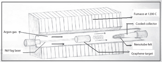
Figure 7.18 Schematic diagram of laser ablation apparatus.
7.7.1.12 Ion Implantation
Ion implantation is an alternative to deposition diffusion and is used to produce a shallow surface region of dopant atoms deposited into a silicon wafer. This technology has made significant inroads into diffusion technology in several areas. In this process a beam of impurity ions is accelerated to kinetic energies in the range of several tens of kV and is directed to the surface of the silicon. As the impurity atoms enter the crystal, they give up their energy to the lattice in collisions and finally come to rest at some average penetration depth, called the projected range, expressed in micrometers. Depending on the impurity and its implantation energy, the range in a given semiconductor may vary from a few hundred angstroms to about one micrometer. Typical distribution of impurity along the projected range is approximately Gaussian. By performing several implantations at different energies, it is possible to synthesize a desired impurity distribution, e.g., a uniformly doped region.
A gas containing the desired impurity is ionized within the ion source. The ions are generated and repelled from their source in a diverging beam that is focused before it passes through a mass separator that directs only the ions of the desired species through a narrow aperture. A second lens focuses this resolved beam, which then passes through an accelerator that brings the ions to their required energy before they strike the target and become implanted in the exposed areas of the silicon wafers. The accelerating voltages may be from 20 kV to as much as 250 kV. In some ion implanters, the mass separation occurs after the ions are accelerated to high energy. Because the ion beam is small, means are provided for scanning it uniformly across the wafers. For this purpose, the focused ion beam is scanned electrostatically over the surface of the wafer in the target chamber (Figure 7.19). Repetitive scanning in a raster pattern provides exceptionally uniform doping of the wafer surface. The target chamber commonly includes automatic wafer handling facilities to speed up the process of implanting many wafers per hour.

Figure 7.19 Schematic of ion implantation system.
7.7.1.13 Synthesis of Nanoporous Polymers Using Membranes
Most of the work in template synthesis has entailed the use of two types of nanoporous membranes: track-etch polymeric membranes and porous alumina membranes.
7.7.1.13.1 Track-Etch Membranes
A number of companies (i.e., Millipore, Nuclepore and Poretics) sell microporous and nanoporous polymeric filtration membranes that have been prepared by the track-etch method [87]. This method entails bombarding a nonporous sheet of the desired material with nuclear fission fragments to create damage tracks in the material, and then chemically etching these tracks into pores. The resulting membranes contain cylindrical pores of uniform diameter which are randomly distributed in the volume of the membrane. Membranes with a wide range of pore diameters (down to 10 nm) and pore densities approaching 109 pores/cm2 are commercially available [87]. The most commonly used materials are polycarbonate or polyester. Other materials, such as mica, are amenable to the track-etch process [88].
7.7.1.13.2 Anodic Alumina Membranes (AAMs)
Porous alumina membranes are electrochemically prepared from an aluminum sheet in an appropriate aqueous solution [89]. The pore structure of a porous alumina membrane is a self-ordered hexagonal array of cells with cylindrical pores of almost uniform diameter and length, which can be controlled by changing the experimental conditions. Pore densities as high as 1011 pores/cm2 can be achieved [87]. Such membranes are commercially available (i.e., Whatman) in a limited number of pore diameters (20, 100, 200 nm). Membranes of this type have also been prepared at the lab scale with pore size as small as 5 nm [87].
7.7.1.13.3 Other Nanoporous Membranes
A variety of other membrane templates have been used. Ionomer membranes have been used as templates for the preparation of various nanoparticles [90]. The ionomer membrane was obtained by wet casting from a solution of the sulfonimide ionomer in dimethylformide, followed by careful annealing at high temperature. Nafion ionomer membranes are provided by DuPont. Biomembranes have been used for template synthesis of nanomaterials, i.e., living biomembrane bi-templates of the mungbean sprout to prepare semiconductor lead selenide nanorods and nanotubes [91], and lamellar DNA-cationic membrane complexes to form CdS nanorods [92]. Mesoporous zeolite membranes have been used for the template synthesis of nanomaterials: polyaniline nanowires have been prepared in the 3-nanometer-wide hexagonal channel system of the aluminosilicate MCM-41 [93].
7.7.2 Chemical Methods
7.7.2.1 Colloidal Methods
Colloidal methods are simple wet chemistry precipitation processes in which solutions of the different ions are mixed under controlled temperature and pressure to form insoluble precipitates. For metal nanoparticles the basic principles of colloidal preparation have been known since antiquity; e.g., gold colloids used for high quality red and purple stained glass from medieval times to date. However, proper scientific investigations of colloidal preparation methods started only in 1857, when Faraday published the results of his experiments with gold. He prepared gold colloids by reduction of HAuCl4 with phosphorus. Today, colloidal processes are widely used to produce such nanomaterials like metals, metal oxides, organics, and pharmaceuticals.
7.7.2.2 Conventional Sol-Gel Method
The sol-gel method is a versatile process used for synthesizing various oxide materials [94]. This synthetic method generally allows control of the textural, chemical, and morphological properties of the solid. This method also has several advantages over other methods, such as allowing impregnation or co-precipitation, which can be used to introduce dopants. The major advantages of the sol-gel technique include molecular scale mixing, high purity of the precursors, and homogeneity of the sol-gel products with a high purity of physical, morphological, and chemical properties [95]. In a typical sol-gel process, a colloidal suspension, or a sol, is formed from the hydrolysis and polymerization reactions of the precursors, which are usually inorganic metal salts or metal organic compounds such as metal alkoxides [96]. A general flowchart for a complete sol-gel process is shown in Figure 7.20. Any factor that affects either or both of these reactions is likely to impact the properties of the gel. These factors, generally referred to as sol-gel parameters, include type of precursor, type of solvent, water content, acid or base content, precursor concentration, and temperature. These parameters affect the structure of the initial gel and, in turn, the properties of the material at all subsequent processing steps. After gelation, the wet gel can be optionally aged in its mother liquor, or in another solvent, and washed. The time between the formation of a gel and its drying, known as aging, is also an important parameter.

Figure 7.20 Schematic diagram of sol-gel method.
7.7.2.3 LB Technique
The Langmuir-Blodgett (LB) technique is a room temperature deposition process that may be used to deposit monolayer and multilayer films of organic materials. Furthermore, this method permits the manipulation of organic molecules on the nanometer scale, thereby allowing intriguing superlattice architectures to be assembled [97]. Advances to the discovery of Langmuir-Blodgett films began with Benjamin Franklin in 1773, when he dropped about a teaspoon of oil onto a pond. Franklin noticed that the waves were calmed almost instantly and that the calming of the waves spread for about half an acre. What Franklin did not realize was that the oil had formed a monolayer on top of the pond surface. Over a century later, Lord Rayleigh quantified what Benjamin Franklin had seen. Knowing that the oil, oleic acid, had spread evenly over the water, Rayleigh calculated that the thickness of the film was 1.6 nm by knowing the volume of oil dropped and the area of coverage.
7.7.2.4 Microemulsion-Based Methods
Ultrafine metal nanoparticles of diameter between 5 nm and 50 nm can be prepared by water-in-oil microemulsions. The nanodroplets of water are dispersed in the oil phase (Figure 7.21). The size of the droplets can be varied in the range of 5–50 nm by changing the water/surfactant ratio. The surfactant molecules provide the sites for particle nucleation and stabilize the growing particles. Therefore, the microemulsion acts as a microreactor.

Figure 7.21 (a) Mechanism for the synthesis of metal nanoparticles by the microemulsion approach, and (b) the percolation mechanism in detail. (Reproduced from [98])
7.7.3 Biosynthesis or Biological Methods of Synthesizing Nanoparticles
The tremendous potential offered by living organisms in biosynthesis of nanometals has spurred encouraging interest. Included in the biological methods is the study of the role of living cells (be it microbes, fungi, actinomycetes, algae or plants) in biosynthesizing nanometals, both intra- as well as extracellularly. The capability of living cells to sequester metal ions and meticulously define the dimensions via fetter-like capping proteins, such as glutathione, phytochelatins and metallothioneins, is intriguing, giving it a monodispersed size. The role of extracellular electron shuttlers in the formation of nanoparticles is also the subject of interest in biogenic synthesis.
The evolutionary challenges and selection pressures over millions of years faced by living organisms have led to the emergence of proficient biological systems and molecules that are adept nanomachines. It took a fraction of a period for scientist to realize the cost-effectiveness and high maintenance of the biosynthetic route for the synthesis of nanometals. Biosynthesis of nanometals is accepted as a “green chemistry” approach. Nature has conferred living systems with proficient processes, endowing them with competency that cannot be aped at lab scale. Many microbes and higher plants are known to possess metal tolerance potential. Due to environmental concerns, ease of synthesis and the need for deft methods for nanometal synthesis, living systems have entered the limelight and are being considered as dexterous candidates for “nanofactories.” There is a plethora of literature available addressing biologically synthesized nanoparticles, which is being added to each day. Some of the literature is listed in Table 7.2.
Table 7.2 Various Organisms That Have Shown the Capacity to Biosynthesize Nanometals.
| Organism | Biosynthesizing organisms | Biosynthesized nanometal | Size (nm) | Ref. |
| Plants | Azadirachta indica Geranium Lemongrass Emblica officinalis Cinnamomum camphora Barbated Skullcup Volvariella volvacea |
Gold | 40–50 20–40 20–30 10–20 65–80 5–30 20–150 |
[99] [100] [99] [101] [102] [103] [104] |
| Emblica officinalis Azadirachta indica Jatropha curcas |
Silver | 10–20 10–20 |
[101] [99] [105] |
|
| Algae | Alfalfa | Ti/Ni Alloy | 2–2.5 | [106] |
| Cylindrotheca fusiformis | Ceramic | NA | [107] | |
| Nitzchia frustulum | Si-Germanium oxide | NA | [108] | |
| Sargassum wightii Fucus vesiculosus |
Gold | 8–12 2–5 |
[109] [110] |
|
| Bacteria | Bacillus subtilis Thiobacillus ferroxidans Lactobacillus spps. Pseudomonas stutzeri ATCC 90271 Rhodopseudomonas capsulate Escherichia coli DH5α |
Gold | 50–100 20–50 100–250 10–20 10–20 10–20 |
[111] [112] [113] [114] [115] [116] |
| Thiobacillus ferroxidans Thiobacillus thioxidans |
Silver sulfide | 200 200 |
[117] [117] |
|
| Pseudomonas stutzeri AG259 Plectonema boryanum Klebsiella pneumonia |
Silver | 200 200 1–6 nm |
[118] [119] [120] |
|
| Klebsiella aerogenes Rhodopseudomonas palustris |
Cadmium sulfide | 20–200 8.01 ± 0.25 |
[121] [122] |
|
| Mycobacterium paratuberculosis Shewanella putrefaciens. Leptothrix ochracea |
Iron | 100 | [123] [124] [125] |
|
| Desulfovibrio desulfuricans D. desulfuricans |
Palladium | 50 50 |
[126] [125] |
|
| Desulfobacteriaceae | Zinc sulfide | 2–5 | [127] | |
| Cyanobacterium spps. and Pseudomonas putida |
Zinc | NA | [128] | |
| Shewanella algae Mixed consortium of sulphate-reducing bacteria |
Platinum | 5 | [129] [130] |
|
| Fungi and Actinomycetes | Yarrowia lipolytica (pH 7 and 9) Verticillium spps Thermomonospora spps. Trichothecium Fusarium oxysporum |
Gold | 20–40 5–10 7–12 10–20 5–10 |
[131] [132] [133] [134] [135] |
| Verticillium spps. Fusarium oxysporum Aspergillus flavus Fusarium semitectum Penicillium fellutanum Penicillium brevicompactum WA 2315 |
Silver | 20–50 2–5 10 10–60 5–25 23–105 |
[136] [137] [138] [139] [140] [141] |
|
| Candida glabrata Schizosaccharomyces pombe |
Cadmium sulfide | 2–5 | [142] | |
| Torulopsis | Lead sulfide | 100–200 | [143] |
7.7.3.1 Nanometal Synthesis Using Microorganisms
By now it is an open secret that microbes take up metal in ionic form and accumulate it within the cell without affecting its regular metabolic activities. This phenomenon is termed “resistance for metal” by microorganisms. But at some stage of the life cycle, if the metal accumulation is uncontrollable by the microorganisms, then the cell produces toxicity, finally leading to the death of the microbe and to the advantage of those who are interested in nanometal synthesis. These microbes die or burst open, releasing nanometals.
Microorganisms have been shown to be important nanofactories that hold immense potential as eco-friendly and cost-effective tools, avoiding toxic, harsh chemicals and the high energy demand required for physiochemical synthesis. Microorganisms have the ability to accumulate and detoxify heavy metals due to various reductase enzymes, which are able to reduce metal salts to metal nanoparticles with a narrow size distribution and, therefore, less polydispersity.
7.7.3.2 Nanometal Synthesis Using Fungi and Actinomycetes
Fungi and actinomycetes have also been stated to be advantageous in the synthesis of nanoparticles [144], which can be scaled up easily, is economically viable, and has the possibility of easily covering large surface areas by suitable growth of the mycelia. This transition from bacteria to fungi as a means of developing natural nanofactories has the added advantage that downstream processing and handling of the biomass would be simpler. To get filtrates from colloidal bacterial broth, sophisticated equipment is a must, whereas filtrates from fungal broths can be obtained by using simple equipment. Fungi have been found to be efficient secretors of soluble proteins and their mutant strains can secrete up to 30 g/l of extracellular protein. It is this character of high level protein secretion that has made fungi a favorite host of heterologous expression of high-value mammalian protein for manufacturing by fermentation.
The ability of fungi and actinomycetes as nanofactories was explored later than bacteria. However, they were found to be more efficient than bacteria. Almost all the nanometals that could be synthesized by bacteria have been successfully biosynthesized also using fungi. The first attempt at biosynthesizing nanometal using fungi was made by Torres-Martínez [145].
7.7.3.3 Nanometals Synthesis Using Plants
Plants respond to heavy metal toxicity in a variety of different ways. Such responses include immobilization, exclusion, chelation and compartmentalization of the metal ions; and the expression of more general stress response mechanisms such as ethylene and stress proteins. These mechanisms have been reviewed comprehensively [146] for plants exposed to cadmium (Cd), the heavy metal for which there has arguably been the greatest number and most wide-ranging studies over many decades. Understanding the molecular and genetic basis for these mechanisms will be an important aspect of developing plants as agents for the phytoremediation of contaminated sites [147]. One recurrent general mechanism for heavy metal detoxification in plants and other organisms is the chelation of the metal by a ligand and, in some cases, the subsequent compartmentalization of the ligand-metal complex. A number of metal binding ligands have now been recognized in plants. The roles of several ligands have been reviewed [148]. Extracellular chelation by organic acids, such as citrate and malate, is important in mechanisms of aluminum tolerance. For example, malate efflux from root apices is stimulated by exposure to aluminum and is correlated with aluminum tolerance in wheat [149]. Some aluminum-resistant mutants of Arabidopsis have also increased organic acid efflux from roots [150]. Organic acids and some amino acids, particularly histidine, also have roles in the chelation of metal ions both within cells and in xylem sap [151]. Peptide ligands include the metallothioneins (MTs), small gene-encoded, cysteine-rich polypeptides. Our current understanding of the functions and expression of MTs in plants, particularly Arabidopsis, have been reviewed elsewhere [148, 152]. In contrast, the phytochelatins (PCs) are enzymatically synthesized cysteine-rich peptides. The PC structure, biosynthesis, and function have been extensively reviewed [148, 153]. Recent advances in our understanding of aspects of PC biosynthesis and function are derived predominantly from molecular genetic approaches using model organisms for the gold and silver nanoparticles synthesis.
7.7.3.4 Nanometals Biosynthesis Using Algae
The capacity of unicellular algae, called diatoms, to take up silica from the surrounding medium and convert it into very fascinating intricate patterns and symmetries on the cell wall has become a field of interest to many materials scientists and has drawn nanotechnologists towards it. Diatoms contain an enzyme called silaffin that can catalyze the polymerization of silica spheres—tiny structures reminiscent of the nanoparticles known to constitute diatom biosilica [154]. Kröger et al., have now further defined the structure of the silaffins and discussed their pivotal role in the nanofabrication of diatom biosilica. A peptide, derived from the silaffin-1A protein of the diatom Cylindrotheca fusiformis, has been found to convert magnesium oxide microfilaments into nanocrystalline magnesium oxide [107]. Fluid (gas or liquid)/silica displacement reactions leading to a variety of other oxides have also been identified. This hybrid (biogenic/synthetic) approach has opened the door to biosculpt ceramic microcomponents with multifarious tailored shapes and compositions for a wide range of environmental, aerospace, biomedical, chemical, telecommunications, automotive, manufacturing, and defense applications. A marine diatom, Nitzschia frustulum, has already been harnessed to fabricate Si-Ge oxide nanocomposite materials [108].
Moreover, apart from diatoms other fresh water as well as marine algae has been successfully used for biosynthesis of nanometals. Singaravelu et al., [109] exploited Sargassum wightii for extracellular synthesis of gold nanoparticles. Oza et al., [155, 156] have also extracellularly synthesized gold nanoparticles using the fresh water algae Chlorella pyrenoidosa and the marine algae Sargassum wightii. Nitrate reductase has been proved to be the most influential reducing enzyme involved in the synthesis of gold nanoparticle by these two algae (Figure 7.22).

Figure 7.22 (a) SEM image of gold nanoparticle synthesized from Sargassum wightii. (b) Schematic representation of nitrate reductase activity in the reduction of gold salt and formation of gold nanoparticles. (Reproduced from [156]; photo courtesy of Madhuri Sharon)
7.7.3.5 Nanometals Biosynthesis Using DNA
The search for unique biogenic nanoparticle synthesis methods led scientists to take advantage of a self-replicating biogenic polymer having high specific interactions between complementary bases in DNA, which evolved into a new branch of technology now known as DNA origami [157, 158]. At present, DNA nanostructures in many cases are formed with DNA origami technology. An alternative method employs nonspecific interactions in DNA solution for the construction of nanosystems. The manipulations with solvent quality via the change in temperature or in solvent composition, pH and ionic strength variation, utilization of ligand binding, and organization of supramolecular structures in a solution can be extended to the manufacturing of DNA nanostructures. DNA is a unique polymer with extremely high charge density and huge bending stiffness. The relatively stable and tough double helix structure, however, can easily be transformed into a flexible single-stranded conformation. This allows us to use the conformational transitions for the formation of multicomponent systems and nanostructures. The specific binding of different ligands with a macromolecule provides the targeted modification of the polymer chain. One of the amazing challenges is to create nanowires and waveguides by the metallization of DNA molecules [159–161]. Two alternative approaches can be used for DNA metallization in a solution and on a substrate: the DNA linking with metallic nanoparticles and the reduction of silver ions after their binding to DNA.
Among biological molecules, DNA has been used extensively as a biotemplate to grow inorganic quantum confined structure and to organize non-biological building blocks into extended hybrid materials because of its physicochemical stability, well-defined sequence of DNA base and a variety of superhelix structures [162]. DNA template has also been described as smart glue for assembling nanoparticles. In general, synthesis of nanoparticles based on DNA template has been done by incubating metal ion-coated DNA in a reduction agent solution. The ion DNA complexes controlled the release of metal ions, slowed down their reduction and effectively inhibited metal ions from growing into big clusters. Nanostructures of metals, such as silver, gold, palladium, platinum, copper, and nickel, have been successfully synthesized by using DNA network templates [162, 163].
7.7.3.6 Nanometals Biosynthesis Using Enzymes
Employment of microbial enzymes for synthesis of gold nanoparticles is a new field with growing importance due to the fact that the enzymatically produced nanoparticles have the potential for use in homogenized catalysts and are suitable for nonlinear optics. The biological agents, including fungi, bacteria and plants, secrete a large amount of enzymes, which are capable of hydrolyzing metals and thus bring about enzymatic reduction of metals ions [164]. There are only a few examples of successful synthesis of nanoparticles using purified microbial enzymes [164–166]. Likewise, the majority of such studies have not examined antimicrobial activity and cytotoxicity of synthesized nanoparticles for biological systems.
7.7.4 Hybrid Methods
There are some methods of fabricating various nanoparticles that utilize a combination of physical, chemical and biological methods. They can be classified under hybrid methods, such as electrochemical, CVD, particle arresting in glass or zeolites, polymers, microemulsion for specific nanomaterials, and microwave radiation-assisted synthesis, especially to eliminate the use of thermal energy utilized for nanoparticle synthesis. Using microwave radiations, carbon quantum dots [167], silver nanoparticles [168] and various TiO2 materials [169] have been synthesized; for example, high-quality rutile rods were developed combining hydrothermal and microwave synthesis, while TiO2 hollow, open-ended nanotubes were synthesized through reacting anatase and rutile crystals in NaOH solution [170, 171].
7.8 Concluding Observations
From the beginning of time to the present, smaller-sized materials have been used for the advancement of nanotechnology. A historical survey of the existence of nanotechnology leads us to believe that, knowingly or unknowingly, this science has existed since prehistoric times. Both nature and human beings have realized the importance of “small,” which has led to an avalanche in the application of nanomaterials by many civilizations that have existed. Nano-size structures have been used in the development of living beings, be it DNA or mitochondria in nature. Man has used nanotechnology for making long-lasting paints, lustrous ceramics, strong metallurgical materials, weather-resistant metals, herbal cosmetics (kaajal), medicines (Bhasmas) and even for deciphering the hidden knowledge of science. With this knowledge we stand at the verge of using this technology for scientific advancements in all scientific domains.
If we take a cursory glance at the perspectives and the future of nanocarbon, it is clear that over the last 20 years, the field of nanoscale carbon has developed exponentially. Since the discovery of fullerenes in 1985, with the bulk synthesis of nanocarbons, the structural identification of nanotubes, the isolation of graphene, and the development of graphene-based applications, we are witnessing an accelerated development of both carbon nanoscience and technology. The number of publications per year in the three nanocarbon fields (fullerenes, nanotubes, and graphene), especially in nanotubes, continues to increase, and it is expected that real applications and devices will soon become an important part of international markets. However, both adoption of reliable standards and addressing biosafety issues need to be put in place, without overregulating, so that fundamental research continues to accelerate while applications keep developing productively.
References
1. Faraday M. The Bakerian Lecture: Experimental Relations of Gold (and Other Metals) to Light. Philos. Trans. R. Soc., 147, 145–181, 1857.
2. Reddy V.R. Gold nanoparticles: Synthesis and applications. Thieme e-Journals, 2006(11), 1791–1792, 2006.
3. Gay-Lussac H. Ueber den Cassius’schen Goldpurpur. Annalen der Physik, 101(8), 629–630, 1832.
4. Berzelius J.J. Ueber den Cassius’ schen Goldpurpur. Annalen der Physik, 98(6), 306–308, 1831.
5. Mie G. Annalen der Physik, 25(3), 377–445, 1908.
6. Madhuri S. J. Nanomed. Res., 2(2), 2015.
7. Gans R. Strahlungsdiagramme ultramikroskopischer Teilchen. Annalen der Physik, 381(1), 29–38, 1925.
8. Aden A.L., Kerker M. Scattering of Electromagnetic Waves from Two Concentric Spheres. J. Appl. Phys., 22(10): 1242–1246, 1951.
9. Bohren C.F., Huffman D.R. Absorption and Scattering of Light by Small Particles. Wiley-VCH Verlag GmbH & Co. KGaA, 1998.
10. Zsigmondy R. Dinglers Polyt. J, 306, 91, 1987.
11. Jain P.K., Huang X., El-Sayed I.H., El-Sayed M.A. Noble metals on the nanoscale: optical and photothermal properties and some applications in imaging, sensing, biology, and medicine. Acc. Chem. Res., 41(12), 1578–1586, 2008.
12. Zhang J.Z., Noguez C. Plasmonic Optical Properties and Applications of Metal Nanostructures. Plasmonics, 3(4), 127–150, 2008.
13. Gramotnev D.K., Bozhevolnyi S.I. Plasmonics beyond the diffraction limit. Nat. Photonics, 4(2), 83–91, 2010.
14. Zeman E.J., Schatz G.C, Zeman Ellen J., Schatz George C. An accurate electromagnetic theory study of surface enhancement factors for silver, gold, copper, lithium, sodium, aluminum, gallium, indium, zinc, and cadmium. J. Phys. Chem., 91(3), 634–643, 1987.
15. Blaber M.G., Arnold M.D., Harris N., Ford M.J., Cortie M.B. Plasmon absorption in nanospheres: A comparison of sodium, potassium, aluminium, silver and gold. Physica B: Condensed Matter, 394(2), 184–187, 2007.
16. McMahon J.M., Schatz G.C., Gray S.K. Plasmonics in the ultraviolet with the poor metals Al, Ga, In, Sn, Tl, Pb, and Bi. Phys. Chem. Chem. Phys., 15(15), 5415–5423, 2013.
17. MK O., Baik H.J., Kim S.K., Park S. J. Mater. Chem., 21, 19069–19073, 2011.
18. Kelly K.L., Coronado E., Zhao L.L., Schatz G.C. The Optical Properties of Metal Nanoparticles: The Influence of Size, Shape, and Dielectric Environment. J. Phys. Chem. B, 107(3), 668–677, 2003.
19. Sosa I.O., Noguez C., Barrera R.G. Optical Properties of Metal Nanoparticles with Arbitrary Shapes. J. Phys. Chem. B, 107(26), 6269–6275, 2003.
20. Lee K.S., El-Sayed M.A. Dependence of the enhanced optical scattering efficiency relative to that of absorption for gold metal nanorods on aspect ratio, size, end-cap shape, and medium refractive index. J. Phys. Chem. B, 109(43), 20331–20338, 2005.
21. Moores A., Goettmann F. The plasmon band in noble metal nanoparticles: an introduction to theory and applications. New J. Chem., 30(8), 1121–1132, 2006.
22. Jain P.K., Lee K.S., El-Sayed I.H., El-Sayed M.A. Calculated absorption and scattering properties of gold nanoparticles of different size, shape, and composition: applications in biological imaging and biomedicine. J. Phys. Chem. B, 110(14), 7238–7248, 2006.
23. Sekhon J.S., Verma S.S. Rational Selection of Nanorod Plasmons: Material, Size, and Shape Dependence Mechanism for Optical Sensors. Plasmonics, 7(3), 453–459, 2012.
24. Blumer H. Zeitschrift für Physik, 119, 32, 1925.
25. Logan N.A. Survey of some early studies of the scattering of plane waves by a sphere. Proc. IEEE, 53(8), 773–785, 1965.
26. Lorenz L. Sur la lumière réfléchie et réfractée par une sphere (surface) transparente In:. Oeuvres scientifiques de L. Lorenz. Lorenz,Copenhague: Revues et annotées par H, Lehmann & Stage,. pp. 403–529, 1898.
27. Grandy W.T. Scattering of Waves from Large Spheres. Cambridge Univ: Cambridge, 2000.
28. Davis E.J., Schweiger G. The Airborne Microparticle. Berlin, Heidelberg: Springer, 2002.
29. Burlak G. The Classical and Quantum Dynamics of the Multispherical Nanostructures. London: Imperial College Press, 2004.
30. Takagahara T., Takeda K. Theory of the quantum confinement effect on excitons in quantum dots of indirect-gap materials. Phys. Rev. B Condens. Matter., 46(23), 15578,1992.
31. Zhao X., Wei C.M., Yang L., Chou M.Y. Phys. Rev. Lett., 92: 23, 2004.
32. Yoffe A.D. Low-dimensional systems: quantum size effects and electronic properties of semiconductor microcrystallites (zero-dimensional systems) and some quasi-two-dimensional systems. Adv. Phys., 42(2), 173–262, 1993.
33. Chen S., Wu Q., Mishra C., Kang J., Zhang H., Cho K, et al. Thermal conductivity of isotopically modified graphene. Nat. Mater., 11(3), 203–207, 2012.
34. Shibata S., Aoki K., Yano T., Yamane M. J. Sol-Gel Sci. Technol., 11(3), 279–287, 1998.
35. Hahn H. Gas phase synthesis of nanocrystalline materials. Nanostruct. Mater., 9(1–8), 3: 3–12, 1997.
36. Cheng H., Ma J., Zhao Z., Qi L. Hydrothermal Preparation of Uniform Nanosize Rutile and Anatase Particles. Chem. Mater., 7(4), 663–671, 1995.
37. Yin H., Wada Y., Kitamura T., Kambe S., Murasawa S., Mori H, et al. Hydrothermal synthesis of nanosized anatase and rutile TiO2 using amorphous phase TiO2. J. Mater. Chem., 11(6), 1694–1703, 2001.
38. Nagaveni K., Hegde M.S., Madras G. Structure and Photocatalytic Activity of Ti1-x Mx O2+δ (M = W, V, Ce, Zr, Fe, and Cu) Synthesized by Solution Combustion Method. J. Phys. Chem. B, 108(52), 20204–20212, 2004.
39. Jones A.C., Chalker P.R. Some recent developments in the chemical vapour deposition of electroceramic oxides. J. Phys. D Appl. Phys., 36(6), R53–R79, 2003.
40. Watson S., Beydoun D., Scott J., Amal R. Preparation of nano-sized crystalline TiO2 particles at low temperature for photocatalysis. J. Nanopart. Res., 6(2/3), 193–207, 2004.
41. Koch C.C., Whittenberger J.D. Mechanical milling/alloying of intermetallics. Intermetallics, 4(5), 339–355, 1996.
42. Janot R., Guérard D. Ball-milling in liquid mediaApplications to the preparation of anodic materials for lithium-ion batteries. Prog. Mater. Sci., 50(1): 1–92, 2005.
43. Tjong S.C., Chen H. Nanocrystalline materials and coatings. Mater. Sci. Eng. R, 45(1–2): 1–88, 2004.
44. Benjamin J.S. Mechanical alloying — A perspective. Metal Powder Report, 45(2), 122–127, 1990.
45. Konrad A., Herr U., Tidecks R., Samwer F. Luminescence of bulk and nanocrystalline cubic yttria Mechanical alloying — A perspective. J. Appl. Phys., 90(7), 3516–3523, 2001.
46. Andrievskii R.A. The synthesis and properties of nanocrystalline refractory compounds. Russ. Chem. Rev., 63(5), 411–427, 1994.
47. Sharma A.B., Sharma M., Pandey R.K. Asian J. Chem, 21(10), S033–038, 2009.
48. Koch C.C. Processing of Metals and Alloys In: Cahn R. W, ed. Materials Science and Technology, A. Comprehensive Treatment. 15. Weinheim, Germany: VCH Verlagsgesellschaft. pp. 193–245, 1991.
49. Benjamin J.S. Metal. Trans, 1, 2943, 1970.
50. Benjamin J.S., Bomford M.J. Dispersion strengthened aluminum made by mechanical alloying. MTA, 8(8), 1301–1305, 1977.
51. Benjamin J.SArzt E, Schultz L, eds. New Materials by Mechanical Alloying Techniques. Oberursel, Germany: DGM Informationgesellschaft. pp. 3–18, 1989.
52. Yang J., Mei S., Ferreira J.M.F. Hydrothermal synthesis of TiO2 nanopowders from tetraalkylammonium hydroxide peptized sols. Mater. Sci. Eng. C, 15(1-2), 183–185, 2001.
53. Carp O., Huisman C.L., Reller A. Photoinduced reactivity of titanium dioxide. Prog. Solid State Chem., 32(1-2), 33–177, 2004.
54. Kim J., Lee J.W., Lee T.G., Nam S.W., Han J. Nanostructured titania membranes with improved thermal stability. J. Mater. Sci., 40(7), 1797–1799, 2005.
55. Iwasaki M., Davis S.A., Mann S. Spongelike Macroporous TiO2 Monoliths Prepared from Starch Gel Template. J. Sol-Gel Sci. Technol., 32(1-3), 99–105, 2004.
56. Bavykin D.V., Friedrich J.M., Walsh F.C. Protonated Titanates and TiO2 Nanostructured Materials: Synthesis, Properties, and Applications. Adv. Mater., 18(21), 2807–2824, 2006.
57. Schulman J.H., Stoeckenius W., Prince L.M. Mechanism of Formation and Structure of Micro Emulsions by Electron Microscopy. J. Phys. Chem., 63(10), 1677–1680, 1959.
58. Boutonnet M., Kizling J., Stenius P., Maire G. The preparation of monodisperse colloidal metal particles from microemulsions. Coll. Surf., 5(3), 209–225, 1982.
59. Yener D.O., Giesche H. Synthesis of Pure and Manganese-, Nickel-, and Zinc-Doped Ferrite Particles in Water-in-Oil Microemulsions. J. Am. Ceram. Soc., 84(9), 1987–1995, 2001.
60. Nanni A., Dei L. Ca(OH)2 Nanoparticles from W/O Microemulsions. Langmuir, 19(3), 933–938, 2003.
61. Gan L.M., Zhang L.H., Chan H.S.O., Chew C.H., Loo B.H. A novel method for the synthesis of perovskite-type mixed metal oxides by the inverse microemulsion technique. Journal Of Materials Science, 31(4), 1071–1079, 1996.
62. Arriagada F.J., Osseo-Asare K. Synthesis of Nanosize Silica in a Nonionic Water-in-Oil Microemulsion: Effects of the Water/Surfactant Molar Ratio and Ammonia Concentration. J. Colloid Interface Sci., 211(2), 210–220, 1999.
63. Uskoković V., Drofenik M. Reverse micelles: Inert nano-reactors or physico-chemically active guides of the capped reactions. Adv. Colloid Interface Sci., 133(1), 23–34, 2007.
64. Levinger N.E. CHEMISTRY: Water in Confinement. Science, 298(5599), 1722–1723, 2002.
65. O’Connor C.J., Kolesnichenko V., Carpenter E., Sangregorio C., Zhou W., Kumbhar A, et al. Fabrication and properties of magnetic particles with nanometer dimensions. Synth. Met., 122(3), 547–557, 2001.
66. Pileni M.-P., Zemb T., Petit C. Solubilization by reverse micelles: Solute localization and structure perturbation. Chem. Phys. Lett., 118(4), 414–420, 1985.
67. Carpenter E.E., Seip C.T., O’Connor C.J. Magnetism of nanophase metal and metal alloy particles formed in ordered phases. J. Appl. Phys., 85(8), 5184–5186, 1999.
68. Powell C.F., Oxley J.H., Blocher Jr J.M. Vapor Deposition. New York: Wiley, 1967.
69. Westwood W.D. AVS Education Committee Book Series. AVS: New York, 2, 2003.
70. Mattox D.M. Film Formation, Adhesion, Surface Preparation In:. Handbook of Physical Vapor Deposition (PVD) Processing. New Jersey: Contamination Control, Noyes Publications, 1998.
71. Geng H. Manufacturing Engineering Handbook. New York: McGraw-Hill, 2004.
72. Helmersson U., Lattemann M., Bohlmark J., Ehiasarian A.P., Gudmundsson J.T. Ionized physical vapor deposition (IPVD): A review of technology and applications. Thin Solid Films, 513(1–2): 1–24, 2006.
73. Uhlenbruck S., Nédélec R., Sebold D., Buchkremer H.P., Stöver D. ECS Transactions, 35, 2275, 2011.
74. Choy K. Chemical vapour deposition of coatings. Prog. Mater. Sci., 48(2): 164–170, 2003.
75. van de Krol R., Goossens A., Schoonman J. Mott-Schottky Analysis of Nanometer-Scale Thin-Film Anatase TiO2. J. Electrochem. Soc., 144(5), 1723–1727, 1997.
76. Endo M., Takeuchi K., Igarashi S., Kobori K., Shiraishi M., Kroto H.W. The production and structure of pyrolytic carbon nanotubes (PCNTs. J. Phys. Chem. Solids, 54(12), 1841–1848, 1993.
77. Dai H., Rinzler A.G., Nikolaev P., Thess A., Colbert D.T., Smalley R.E. Single-wall nanotubes produced by metal-catalyzed disproportionation of carbon monoxide. Chem. Phys. Lett., 260(3-4), 471–475, 1996.
78. Kim C.S., Okuyama K., Nakaso K., Shimada M. Direct Measurement of Nucleation and Growth Modes in Titania Nanoparticles Generation by a CVD Method. J. Chem. Eng. Japan /. JCEJ., 37(11), 1379–1389, 2004.
79. Cao Y., Yang W., Zhang W., Liu G., Yue P. New J. Chem., 2(8), 218–222, 2004.
80. Gracia F., Holgado J.P., Caballero A., Gonzalez-Elipe A.R. Structural, Optical, and Photoelectrochemical Properties of M n+–TiO2 Model Thin Film Photocatalysts. J. Phys. Chem. B, 108(45), 17466–17476, 2004.
81. Kim C.S., Nakaso K., Xia B., Okuyama K., Shimada M. A New Observation on the Phase Transformation of TiO2 Nanoparticles Produced by a CVD Method. Aerosol Sci. Technol., 39(2), 104–112, 2005.
82. Liang C., Shimizu Y., Sasaki T., Koshizaki N. Synthesis, characterization, and phase stability of ultrafine TiO2 nanoparticles by pulsed laser ablation in liquid media. J. Mater. Res., 19(5), 1551–1557, 2004.
83. Chopra K.L. Thin Film Phenomena. New York: McGraw-Hill, 1969.
84. Cockyane B., Wright P.J. Metalorganic chemical vapour deposition of wide band gap II–VI compounds. J. Cryst. Growth, 68(1), 223–230, 1984.
85. Guo T., Nikolaev P., Thess A., Colbert D.T., Smalley R.E. Catalytic growth of single-walled manotubes by laser vaporization. Chem. Phys. Lett., 243(1–2), 49–54, 1995.
86. Thess A., Lee R., Nikolaev P., Dai H., Petit P., Robert J, et al. Crystalline Ropes of Metallic Carbon Nanotubes. Science, 273(5274), 483–487, 1996.
87. Martin C.R. Membrane-Based Synthesis of Nanomaterials. Chem. Mater., 8(8), 1739–1746, 1996.
88. Huczko A. Template-based synthesis of nanomaterials. Appl. Phys. A, 70(4), 365–376, 2000.
89. Schmid G. Materials in nanoporous alumina. J. Mater. Chem., 12(5), 1231–1238, 2002.
90. Rollins H.W., Whiteside T., Shafer G.J., Ma J.-J., Tu M.-H., Liu J.-T, JJ M,, et al. Nanoscale metal sulfides in perfluorinated ionomer membranes. J. Mater. Chem., 10(9), 2081–2084, 2000.
91. Li L., Wu Q.-S., Ding Y.-P. Living bio-membrane bi-template route for simultaneous synthesis of lead selenide nanorods and nanotubes. Nanotechnology, 15(12), 1877–1881, 2004.
92. Liang H., Angelini T.E., Ho J., Braun P.V., Wong G.C. Molecular imprinting of biomineralized CdS nanostructures: crystallographic control using self-assembled DNA-membrane templates. J. Am. Chem. Soc., 125(39), 11786–11787, 2003.
93. Wu C.G., Bein T. Conducting polyaniline filaments in a mesoporous channel host. Science, 264(5166), 1757–1759, 1994.
94. Fernández-García M., Martínez-Arias A., Hanson J.C., Rodriguez J.A. Nanostructured oxides in chemistry: characterization and properties. Chem. Rev., 104(9), 4063–4104, 2004.
95. Kolen’ko Y.V., Kovnir K.A., Gavrilov A.I., Garshev A.V., Meskin P.E., Churagulov B.R, et al. Structural, textural, and electronic properties of a nanosized mesoporous ZnxTi1-xO2-) solid solution prepared by a supercritical drying route. J. Phys. Chem. B, 109(43), 20303–20309, 2005.
96. Pierre A.C. Introduction to Sol-Gel Processing. Boston: Kluwer Academic Publishers. p. 394, 1998.
97. Petty M.C. Langmuir-Blodgett Films In:. An Introduction. Cambridge: Cambridge University Press, 1996.
98. Capek I. Preparation of metal nanoparticles in water-in-oil (w/o) microemulsions. Adv. Colloid Interface Sci., 110(1–2), 49–74, 2004.
99. Shankar S.S., Rai A., Ahmad A., Sastry M. Rapid synthesis of Au, Ag, and bimetallic Au core-Ag shell nanoparticles using Neem (Azadirachta indica) leaf broth. J. Colloid Interface Sci., 275(2), 496–502, 2004.
100. Shankar S.S., Rai A., Ankamwar B., Singh A., Ahmad A., Sastry M. Biological synthesis of triangular gold nanoprisms. Nat. Mater., 3(7), 482–488, 2004.
101. Ankamwar B., Damle C., Ahmad A., Sastry M. J. Nanosci. Nanotech, 5, 1665–1671, 2005.
102. Huang J., Li Q., Sun D., Lu Y., Su Y., Yang X, et al. Biosynthesis of silver and gold nanoparticles by novel sundried Cinnamomum camphora leaf. Nanotechnology, 18(10): 105104, 2007.
103. Wang Y., He X., Wang K., Zhang X., Tan W. Barbated Skullcup herb extract-mediated biosynthesis of gold nanoparticles and its primary application in electrochemistry. Colloids Surf. B Biointerfaces, 73(1), 75–79, 2009.
104. Philip D. Biosynthesis of Au, Ag and Au-Ag nanoparticles using edible mushroom extract. Spectrochim. Acta A Mol. Biomol. Spectrosc., 73(2), 374–381, 2009.
105. Bar H., Bhui D.K., Sahoo G.P., Sarkar P., De S.P., Misra A. Green synthesis of silver nanoparticles using latex of Jatropha curcas. Colloids Surf. A Physicochem. Eng. Aspects, 339(1-3), 134–139, 2009.
106. Schabes-Retchkiman P.S., Canizal G., Herrera-Becerra R., Zorrilla C., Liu H.B., Ascencio J.A. Biosynthesis and characterization of Ti/Ni bimetallic nanoparticles. Opt. Mater. (Amst)., 29(1), 95–99, 2006.
107. Dickerson M.B., Naik R.R., Sarosi P.M., Agarwal G., Stone M.O., Sandhage K.H. Ceramic nanoparticle assemblies with tailored shapes and tailored chemistries via biosculpting and shape-preserving inorganic conversion. J. Nanosci. Nanotechnol., 5(1), 63–67, 2005.
108. Rorrer G.L., Chang C.H., Liu S.H., Jeffryes C., Jiao J., Hedberg J.A. Biosynthesis of silicon-germanium oxide nanocomposites by the marine diatom Nitzschia frustulum. J. Nanosci. Nanotechnol., 5(1), 41–49, 2005.
109. Singaravelu G., Arockiamary J.S., Kumar V.G., Govindaraju K. A novel extracellular synthesis of monodisperse gold nanoparticles using marine alga, Sargassum wightii Greville. Colloids Surf. B Biointerfaces, 57(1), 97–101, 2007.
110. Mata Y.N., Torres E., Blázquez M.L., Ballester A., González F., Muñoz J.A. Gold(III) biosorption and bioreduction with the brown alga Fucus vesiculosus. J. Hazard. Mater., 166(2–3), 612–618, 2009.
111. Beveridge T.J., Murray R.G. Sites of metal deposition in the cell wall of Bacillus subtilis. J. Bacteriol., 141(2), 876–887, 1980.
112. Belly R.T., Kydd G.C. Dev. Ind. Microbiol. 2. pp. 567–577, 1982.
113. Nair B., Pradeep T. Coalescence of Nanoclusters and Formation of Submicron Crystallites Assisted by Lactobacillus Strains.
Cryst. Growth Des., 2(4), 293–298, 2002.
114. Husseiny M.I., El-Aziz M.A., Badr Y., Mahmoud M.A. Biosynthesis of gold nanoparticles using Pseudomonas aeruginosa. Spectrochim. Acta A Mol. Biomol. Spectrosc., 67(3-4), 1003–1006, 2007.
115. He S., Guo Z., Zhang Y., Zhang S., Wang J., Gu N. Biosynthesis of gold nanoparticles using the bacteria Rhodopseudomonas capsulata. Mater. Lett., 61(18), 3984–3987, 2007.
116. Du L., Jiang H., Liu X., Wang E. Biosynthesis of gold nanoparticles assisted by Escherichia coli DH5α and its application on direct electrochemistry of hemoglobin. Electrochem. commun., 9(5), 1165–1170, 2007.
117. Pooley F.D. Bacteria accumulate silver during leaching of sulphide ore minerals. Nature, 296(5858), 642–643, 1982.
118. Klaus T., Joerger R., Olsson E., Granqvist C.G. Silver-based crystalline nanoparticles, microbially fabricated. Proc. Natl. Acad. Sci. U.S.A., 96(24), 13611–13614, 1999.
119. Lengke M.F., Fleet M.E., Southam G. Biosynthesis of silver nanoparticles by filamentous cyanobacteria from a silver(I) nitrate complex. Langmuir, 23(5), 2694–2699, 2007.
120. Mokhtari N., Daneshpajouh S., Seyedbagheri S., Atashdehghan R., Abdi K., Sarkar S, et al. Biological synthesis of very small silver nanoparticles by culture supernatant of Klebsiella pneumonia: The effects of visible-light irradiation and the liquid mixing process. Mater. Res. Bull., 44(6), 1415–1421, 2009.
121. Holmes J.D., Richardson D.J., Saed S., Evans-Gowing R., Russell D.A., Sodeau J.R. Cadmium-specific formation of metal sulfide ‘Q-particles’ by Klebsiella pneumoniae. Microbiology, 143 (Pt 8, 2521–2530, 1997.
122. Bai H.J., Zhang Z.M., Guo Y., Yang G.E. Biosynthesis of cadmium sulfide nanoparticles by photosynthetic bacteria Rhodopseudomonas palustris. Colloids Surf. B Biointerfaces, 70(1), 142–146, 2009.
123. Homuth M., Valentin-Weigand P., Rohde M., Gerlach G.F. Identification and characterization of a novel extracellular ferric reductase from Mycobacterium paratuberculosis. Infect. Immun., 66(2), 710–716, 1998.
124. Newman D.K., Kolter R. A role for excreted quinones in extracellular electron transfer. Nature, 405(6782), 94–97, 2000.
125. Hashimoto H., Yokoyama S., Asaoka H., Kusano Y., Ikeda Y., Seno M., Takada J, et al. Characteristics of hollow microtubes consisting of amorphous iron oxide nanoparticles produced by iron oxidizing bacteria, Leptothrix ochracea. J. Magn. Magn. Mater., 310(2), 2405–2407, 2007.
126. Lloyd J.R., Yong P., Macaskie L.E. Enzymatic recovery of elemental palladium by using sulfate-reducing bacteria. Appl. Environ. Microbiol., 64(11), 4607–4609, 1998.
127. Butt T.R., Ecker D.J. Yeast metallothionein and applications in biotechnology. Microbiol. Rev., 51(3), 351–364, 1987.
128. Higham D.P., Sadler P.J., Scawen M.D. J. Gen. Microbiol., 131, 2539–2544, 1985.
129. Konishi Y., Ohno K., Saitoh N., Nomura T., Nagamine S., Hishida H, et al. Bioreductive deposition of platinum nanoparticles on the bacterium Shewanella algae. J. Biotechnol., 128(3), 648–653, 2007.
130. Riddin T.L., Govender Y., Gericke M., Whiteley C.G. Enzyme Microb. Technol., 38, 291–316, 2006.
131. Agnihotri M., Joshi S., Kumar A.R., Zinjarde S., Kulkarni S. Biosynthesis of gold nanoparticles by the tropical marine yeast Yarrowia lipolytica NCIM 3589. Mater. Lett., 63(15), 1231–1234, 2009.
132. Ahmad A., Senapati S., Khan M.I., Kumar R., Sastry M. Extracellular Biosynthesis of Monodisperse Gold Nanoparticles by a Novel Extremophilic Actinomycete, Thermomonospora sp. Langmuir, 19(8), 3550–3553, 2003.
133. Ahmad A., Senapati S., Khan M.I., Kumar R., Ramani R., Srinivas V, et al. Intracellular synthesis of gold nanoparticles by a novel alkalotolerant actinomycete, Rhodococcus species. Nanotechnology, 14(7), 824–828, 2003.
134. Ahmad A., Senapati S., Khan M.I., Kumar R., Sastry M. Extra-/Intracellular Biosynthesis of Gold Nanoparticles by an Alkalotolerant Fungus, Trichothecium sp. J. Biomed. Nanotechnol., 1(1), 47–53, 2005.
135. Mukherjee P., Senapati S., Mandal D., Ahmad A., Khan M.I., Kumar R, et al. Chem Biochem, 3, 461–463, 2002.
136. Mukherjee P., Ahmad A., Mandal D., Senapati S., Sainkar S.R., Khan M.I, et al. Bioreduction of AuCl4– Ions by the Fungus, Verticillium sp. and Surface Trapping of the Gold Nanoparticles Formed D.M. and S.S. thank the Council of Scientific and Industrial Research (CSIR), Government of India, for financial assistance. Angew. Chem. Int. Ed., 40(19), 3585–3588, 2001.
137. Durán N., Marcato P.D., Alves O.L., Souza G.I., Esposito E. Mechanistic aspects of biosynthesis of silver nanoparticles by several Fusarium oxysporum strains. J. Nanobiotechnology, 3(1), 8–12, 2005.
138. Vigneshwaran N., Ashtaputre N.M., Varadarajan P.V., Nachane R.P., Paralikar K.M., Balasubramanya R.H. Biological synthesis of silver nanoparticles using the fungus Aspergillus flavus. Mater. Lett., 61(6), 1413–1418, 2007.
139. Basavaraja S., Balaji S.D., Lagashetty A., Rajasab A.H., Venkataraman A. Extracellular biosynthesis of silver nanoparticles using the fungus Fusarium semitectum. Mater. Res. Bull., 43(5), 1164–1170, 2008.
140. Kathiresan K., Manivannan S., Nabeel M.A., Dhivya B. Studies on silver nanoparticles synthesized by a marine fungus, Penicillium fellutanum isolated from coastal mangrove sediment. Colloids Surf. B Biointerfaces, 71(1), 133–137, 2009.
141. Shaligram N.S., Bule M., Bhambure R., Singhal R.S., Singh S.K., Szakacs G, et al. Biosynthesis of silver nanoparticles using aqueous extract from the compactin producing fungal strain. Process Biochemistry, 44(8), 939–943, 2009.
142. Dameron C.T., Reese R.N., Mehra R.K., Kortan A.R., Carroll P.J., Steigerwald M.L, et al. Biosynthesis of cadmium sulphide quantum semiconductor crystallites. Nature, 338(6216), 596–597, 1989.
143. Kowshik M., Deshmukh N., Vogel W., Urban J., Kulkarni S.K., Paknikar K.M. Microbial synthesis of semiconductor CdS nanoparticles, their characterization, and their use in the fabrication of an ideal diode. Biotechnol. Bioeng., 78(5), 583–588, 2002.
144. Sastry M., Ahmad A., Khan M.I., Kumar R. Curr. Sci., 85, 162–170, 2003.
145. Torres-Martínez C.L., Nguyen L., Kho R., Bae W., Bozhilov K., Klimov V, et al. Biomolecularly capped uniformly sized nanocrystalline materials: glutathione-capped ZnS nanocrystals. Nanotechnology, 10(3), 340–354, 1999.
146. Sanità di Toppi L., Gabbrielli R. Response to cadmium in higher plants. Environ. Exp. Bot., 41(2), 105–130, 1999.
147. Salt D.E., Smith R.D., Raskin I. Phytoremediation. Annu. Rev. Plant Physiol. Plant Mol. Biol., 49, 643–668, 1998.
148. Rauser W.E. Structure and function of metal chelators produced by plants: the case for organic acids, amino acids, phytin, and metallothioneins. Cell Biochem. Biophys., 31(1), 19–48, 1999.
149. Delhaize E., Ryan P.R. Aluminum Toxicity and Tolerance in Plants. Plant Physiol., 107(2), 315–321, 1995.
150. Larsen P.B., Degenhardt J., Tai C.Y., Stenzler L.M., Howell S.H., Kochian L.V. Aluminum-resistant Arabidopsis mutants that exhibit altered patterns of aluminum accumulation and organic acid release from roots. Plant Physiol., 117(1), 9–17, 1998.
151. Krämer U., Cotter-Howells J.D., Charnock J.M., Baker A.J.M., Smith J.A.C. Free histidine as a metal chelator in plants that accumulate nickel. Nature, 379(6566), 635–638, 1996.
152. Fordham-Skelton A.P., Robinson N.J., Goldsbrough P.B,Silver S, Walden W, eds. Metal Ions in Gene Regulation. London: Chapman and Hall. p. 398, 1998.
153. Zenk M.H. Heavy metal detoxification in higher plants–a review. Gene, 179(1), 21–30, 1996.
154. Kröger N., Deutzmann R., Bergsdorf C., Sumper M. Species-specific polyamines from diatoms control silica morphology. Proc. Natl. Acad. Sci. U.S.A., 97(26), 14133–14138, 2000.
155. Oza G., Pandey S., Mewada A., Kalita G., Madhuri S. Adv. Appl. Sci. Res, 3(3), 1405–1412, 2012.
156. Oza G., Pandey S., Shah R., Madhuri S. Euro. J. Exp. Bio, 2(3), 505–512, 2012.
157. Rothemund P.W. Folding DNA to create nanoscale shapes and patterns. Nature, 440(7082), 297–302, 2006.
158. Douglas S.M., Dietz H., Liedl T., Högberg B., Graf F., Shih W.M. Self-assembly of DNA into nanoscale three-dimensional shapes. Nature, 459(7245), 414–418, 2009.
159. Klein W.P., Schmidt C.N., Rapp B., Takabayashi S., Knowlton W.B., Lee J, et al. Multiscaffold DNA origami nanoparticle waveguides. Nano Lett., 13(8), 3850–3856, 2013.
160. Watson S.M., Pike A.R., Pate J., Houlton A., Horrocks B.R. DNA-templated nanowires: morphology and electrical conductivity. Nanoscale, 6(8), 4027–4037, 2014.
161. Puchkova A.O., Sokolov P., Petrov Y.V., Kasyanenko N.A. Metallization of DNA on silicon surface. J. Nanopart. Res., 13(9), 3633–3641, 2011.
162. Braun E., Eichen Y., Sivan U., Ben-Yoseph G. DNA-templated assembly and electrode attachment of a conducting silver wire. Nature, 391(6669): 775–778, 1998.
163. Yao Y., Song Y., Wang L. Synthesis of CdS nanoparticles based on DNA network templates. Nanotechnology, 19(40): 405601, 2008.
164. Xie X., Xu W., Liu X. Improving colorimetric assays through protein enzyme-assisted gold nanoparticle amplification. Acc. Chem. Res., 45(9), 1511–1520, 2012.
165. Riddin T.L., Govender Y., Gericke M., Whiteley C.G. Two different hydrogenase enzymes from sulphate-reducing bacteria are responsible for the bioreductive mechanism of platinum into nanoparticles. Enzyme Microb. Technol., 45(4), 267–273, 2009.
166. Gholami-Shabani M., Akbarzadeh A., Norouzian D., Amini A., Gholami-Shabani Z., Imani A, et al. Antimicrobial activity and physical characterization of silver nanoparticles green synthesized using nitrate reductase from Fusarium oxysporum. Appl. Biochem. Biotechnol., 172(8), 4084–4098, 2014.
167. Mewada A., Pandey S., Shinde S., Mishra N., Oza G., Thakur M, et al. Green synthesis of biocompatible carbon dots using aqueous extract of Trapa bispinosa peel. Mater. Sci. Eng. C Mater. Biol. Appl., 33(5), 2914–2917, 2013.
168. Pandey S., Mewada A., Thakur M., Shinde S., Shah R., Oza G, et al. J. Nanosci, 2013.
169. Corradi A.B., Bondioli F., Focher B., Ferrari A.M., Grippo C., Mariani E, et al. Conventional and Microwave-Hydrothermal Synthesis of TiO2 Nanopowders. J. American Ceramic Society, 88(9), 2639–2641, 2005.
170. Ma G., Zhao X., Zhu J. Int. J. Mod. Phys. B, 19, 15–17, 2005.
171. Wu X., Jiang Q.-Z., Ma Z.-F., Fu M., Shangguan W.-F. Synthesis of titania nanotubes by microwave irradiation. Solid State Commun., 136(9-10), 513–517, 2005.