
6 Image sensors
The digital image sensor is considered in many ways the ‘heart’ of an image capture device. These silicon chips are about the size of a fingernail and contain millions of photosensitive elements called photosites. They convert light imaged through the camera lens into electrical signals which are then processed to form a two-dimensional image representing the scene being captured. In this chapter the operation of a digital image sensor will be described. You will learn how photons striking a sensor are converted to electric charge. A photon is a single packet of energy that defines light. To capture an image, millions of tiny photosites are combined into a two-dimensional array, each of which transforms the light from one point of the image into electrons. A description of the different arrangements used for transferring charge from the sensor will be given. A basic image sensor is only capable of ‘seeing’ a monochrome image. The most commonly used methods for enabling a sensor to capture colour are presented, and these include the Bayer colour filter array and the Foveon sensor array. Recent advances in sensor technology including back illuminated sensors and a high sensitivity colour filter array from Kodak are described. Details about sensor fill factor, microlenses and sensor dimensions are discussed. Image sensors are not perfect imaging devices and can introduce artefacts into the captured image. This chapter will present some of the more common artefacts associated with the application of imaging sensors. Noise, blooming and moiré effects, for example, are some of the best-known and studied image sensor artefacts. Another artefact, more commonly associated with modern digital single-lens reflex (DSLR) systems, is caused by dust which can adhere to the sensor. Sensor specifications are an important consideration when choosing which digital camera to buy. The sensor specification will govern the type of lens required by the camera, the resolution of the captured images and the level of artefacts seen in the image.
An introduction to image sensors
The image sensor in a digital camera converts light coming from the subject being photographed into an electronic signal which is eventually processed into a digital photograph that can be displayed or printed. There are, broadly speaking, two main types of sensor in use today: the charge-coupled device (CCD) and the complementary metal oxide semiconductor (CMOS) sensor. The technology behind CCD image sensors was developed in the late 1960s, when scientists George Smith and Willard Boyle at Bell Labs were attempting to create a new type of semiconductor memory for computers. In 1970 the CCD had been built into the first ever solid-state video camera. These developments began to shape the revolution in digital imaging. Today, CCDs can be found in astronomical and many other scientific applications. One of the fundamental differences between CCD and CMOS sensors is that CMOS sensors convert charge to voltage at each photoelement, whereas in a CCD the conversion is done in a common output amplifer. This meant that during the early development of the sensors, the CCD had a quality advantage over the CMOS. As a result CMOS sensors were largely overlooked for serious imaging applications until the late 1990s. Today, the performance difference between the sensor types has diminished and CMOS sensors are used in devices ranging from most camera phones to some professional DSLRs. Major advantages of CMOS sensors over CCDs include their low power consumption, low manufacturing cost, and higher level of ‘intelligence’ and functionality built into the chip. In the consumer and prosumer market today, CCDs continue to be used today due to their greater light sensitivity, dynamic range and noise performance. The Foveon sensor is based on CMOS technology and uses a three-layer design to capture red-, green- and blue-coloured light at each pixel. The Foveon X3 sensor is used in Sigma DSLR cameras designed by the company. A closer look at the Foveon sensor is given later in this chapter. The Live MOS sensor is a new generation of sensor that claims to offer the high image quality of a CCD sensor combined with the low power consumption of the CMOS sensor. It is used by Panasonic and Olympus in their range of DSLR cameras. More discussion on the different aspects of sensors can be found in Chapter 2.
Converting photons to charge
Image sensors are capable of responding to a wide variety of light sources, ranging from X-rays through to infrared wavelengths, but sensors used in digital cameras are tuned largely to the visible range of the spectrum – that is, to wavelengths between 380 and 700 nm. Sensors rely on semiconductor materials to convert captured light into an electrical charge. This is done in much the same way as a solar cell does on a solar-powered calculator. A semiconductor is formed when silicon, which is a very poor conductor, is doped with an impurity to improve its conductivity, hence the name semiconductor. Light reaching the semiconductor with wavelengths shorter than 1100 nm is absorbed and a conversion from photon to electrical charge takes place. This happens when the light provides energy which releases negatively charged electrons from silicon atoms. Note that light with wavelengths shorter than about 380 nm is essentially blocked by the silicon while light with wavelength greater than 1100 nm passes through the silicon practically uninterrupted. The response of a sensor in the infrared region is reduced in colour digital still cameras (DSCs) by using an infrared-absorbing filter. Such filters are placed between the imaging lens and the sensor (see Figure 6.1). The basic building block of a CCD sensor is the picture element, or pixel. Each pixel includes a photodetector, which can be either a metal oxide semiconductor (MOS) capacitor or a photodiode. Each pixel also includes a readout structure. In a CCD, one or more light-shielded MOS capacitors are used to read out the charge from each pixel. In a CMOS sensor, several transistors are used to amplify the signal and connect the amplifed signal to a readout line as the image is scanned out. The photodetectors of each pixel become electrically charged to a level that is directly proportional to the amount of light that it receives over a given period of time. This period is known as the integration time. A ‘potential well’ is formed at each photosite, and the positive potential of the well collects the electron charges over the period defined by the integration time. The capacity of the well is restricted and as a result a ‘drain’ circuit is normally included to prevent charge from migrating to neighbouring photosites, which can otherwise result in undesirable image artefacts such as blooming. You will read more about these artefacts later in this chapter. Photosite sensitivity is
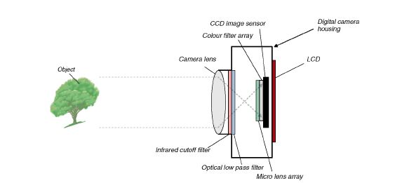
Figure 6.1 A simplifed cross-sectional diagram showing the typical positioning of components in a digital still camera. Light from the object being photographed is projected on to the sensor by the camera lens.
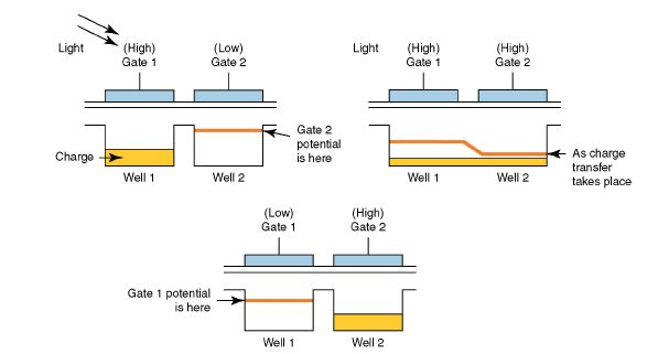
Figure 6.2 A cross-sectional diagram showing the charge transfer process.
dependent on the maximum charge that can be accumulated as well as the effciency with which photons that are incident on the sensor are converted into charge.
Once charge has accumulated in the potential well of the photodiode or photocapacitor, a clock circuit increases the potential of the adjacent structure, causing the charge from the photodetector to be transferred to the adjacent well. Figure 6.2 shows how charge transfer occurs between two wells. The clock signals that are applied to the gates take the form of complementary square-wave voltage signals. When the voltage at Gate 1 is high, and the voltage at Gate 2 is low, photo-electrons are collected at the Gate 1 well. When the high voltage begins to be applied at Gate 2, and the voltage at Gate 1 falls, charge fows from Well 1 into Well 2. (Note – the low potential is usually a negative voltage, not zero volts.) This process by which charge is transferred between wells is where the CCD gets its name. By arranging the MOS capacitors in a series (known as a CCD register) and by manipulating the gate voltages appropriately, charge can be transferred from one gate to the next and eventually to a common charge to voltage conversion circuit that provides the sensor output signal. This serial transfer of charge out of a CCD is sometimes described as a ‘bucket brigade’, where similarity is drawn to the bucket brigade of a traditional (old-flashioned) fire department.
The mechanisms by which CMOS sensors convert incident light into charge are fundamentally similar to those used by CCD sensors. The two sensors, however, diverge considerably in the way that charge is transferred off the chip.
Array architectures
In this section you will learn about the different ways that photosites are arranged in order that a two-dimensional image can be generated.
CCD sensors
An arrangement that is suited to flatbed document and film scanners is to place the photosites along a single axis in such a way that scanning can only take place in a single direction. A stepper motor is used to position the array over the document or film (or to transport the film) and a single line of data is captured and read out of the array using the charge transfer process described above. The array is then repositioned and the data capture process is repeated. Limitations in the physical length of the array due to device fabrication constraints can be overcome by placing several linear CCDs adjacent to one another, thereby increasing the overall length of the sensor. The time taken to scan an A4-sized document or a frame of 35 mm film can range from a fraction of a second to several minutes. For this reason, linear scanners are unsuitable for use in a digital still camera, except for a few specialized applications such as still-life photography.
All area array sensors are based on arranging photosites on an x–y orthogonal grid. Area array sensors are the most appropriate arrangement for digital camera systems. A photograph of an area array CCD sensor is shown in Figure 6.3. The most popular CCD array architectures are the ‘frame transfer’ (FT) array and the ‘interline transfer’ (IT) array.
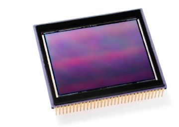
Figure 6.3 A CCD sensor.
Frame transfer arrays are the simplest of all the CCD architectures and have the added benefit that they are also the easiest to fabricate and operate. A diagram of an FT array is shown in Figure 6.4. The array comprises an imaging area, a charge storage area and a serial readout register array. The imaging array is formed from an array of photosites, or pixels, arranged such that charge can be transferred in parallel vertically (vertical CCD). The entire pixel is dedicated to image capture in this architecture. The charge storage area is identical to the imaging array except for the fact that it is masked by a metal shield that prevents light from reaching the photosites. After
exposure to light, charge is quickly transferred into the storage area. It is subsequently transferred one line at a time to the horizontal CCD and then serially to the output charge to voltage converter (shown in green). Image smear can be a problem with this type of array and this can result when the charge integration period (exposure time) overlaps with the transfer time to the storage array. The design of the frame transfer array can be simplifed further by eliminating the charge storage array. To prevent light from reaching the imaging area while charge is being transferred to the horizontal CCD, a mechanical shutter is fitted between the lens and the sensor. This has the added benefit of reducing smear which can occur during the charge transfer. This type of sensor is known as a full-frame (FF) array. Full-frame arrays are used in higher-end digital cameras such as DSLRs.
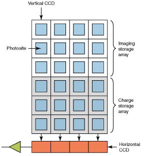
Figure 6.4 A diagram of a frame transfer array. Two arrays are used, one for imaging and the other for storage. Following exposure, photoelectrons are transferred rapidly from the imaging array to the light-shielded storage array. Data is then read out line by line to a serial register and off the chip for processing.
The second type of CCD architecture is the IT array. A diagram of an IT array is shown in Figure 6.5. In this type of array each pixel has both a photodiode and an associated charge storage area. The charge storage area is a vertical CCD that is shielded from light and is only used for the charge transfer process. After exposure, the charge is transferred from the photodiode into the charge storage area in the order of microseconds. Once in the storage area the charge is transferred to the horizontal CCD register and converted to an output voltage signal in much the same way as the FT array described above. One of the advantages of the interline design is that it is possible to re-expose the photodiode to light very soon after charge is transferred into the storage area, thereby enabling video to be captured. IT arrays are the most commonly used array architecture in digital cameras today. Their ability to capture video enhances the functionality of the digital camera. Users are able to compose an image on the LCD fitted to the camera as well as being able to capture short segments (clips) of video. (Note – IT can also have smear (leakage) from the photodiode into the vertical register as the previous frame is clocked out. A shutter is normally used to eliminate this smear and to enable the sensor to use interlaced readout.) The main disadvantage of the IT architecture is that a significant portion of the sensor is now allocated to frame storage and, by definition, is no longer light sensitive. The ratio of the photosensitive area inside a pixel to the pixel area is impacted as a result. This ratio is known as the pixel ‘fill factor’. A diagram showing the top view of a pixel from an IT array is shown in Figure 6.6. The proportion of photosensitive area relative to the charge storage area is typically in the region of 30–50%. A lower fill factor reduces the sensitivity of the pixel and can lead to higher noise and lower resolution. Later in the chapter you will read about ways in which the effective fill factor can be improved by adding a small lens (microlens) to each photosite.
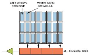
Figure 6.5 A diagram of an interline transfer array. Photosites comprise a photodiode and a light-shielded storage area. Charge is transferred from the photodiode to the storage area after exposure. It is then transferred off the chip to the horizontal CCD.

Figure 6.6 A simplified diagram showing the top view of a photosite from aninterline transfer array.

Figure 6.7 A diagram showing the arrangement of a photodiode and on-chip amplifer in a CMOS array sensor.
CMOS sensors
Most CMOS sensors today employ a technology in which both the photodiode and a readout amplifer are incorporated into a pixel. This technology is known as ‘active pixel sensor’ (APS). Unlike the CCD, the charge accumulated at each photosite in a CMOS sensor is converted into an analogue voltage in each pixel and the voltage from each pixel is connected to a common readout line using switching transistors in each pixel. The photodiode and associated
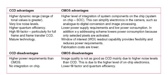
Figure 6.8 The advantages and disadvantages of CCD and CMOS sensors.
amplification circuitry are arranged on an x–y grid as shown in Figure 6.7. An important advantage in the design of the CMOS array is that, unlike the CCD sensor array, charge from each pixel can be read out independently from other pixels in the array. This x–y pixel addressing scheme means that it is possible to read out portions (windows) of the array which can be used for advanced image-processing applications in the camera such as light metering, autofocusing or image stabilization. The advantages and disadvantages of CCDs and CMOS sensors are summarized in the table shown in Figure 6.8.
Canon was one of the first manufacturers to introduce CMOS sensors into DSLRs. The first DSLR with a CMOS sensor was the prosumer Canon EOS D30 in 2000. Today, CMOS sensors are finding their way into professional DSLRs. One example is the Canon 1Ds MK III, which uses a 21.1 megapixel CMOS sensor. The sensor size in this camera is equivalent to the size of a single frame of 35 mm film. Larger sensor sizes help improve fill factor and reduce the higher noise levels that exist due to the additional on-chip electronics. Cameras in low-power devices such as mobile phones, webcams and personal digital assistants (PDAs) have, for many years now, been fitted with CMOS sensors. The sensors can be fabricated cost-effectively with very small dimensions. Traditionally, the quality of images delivered by these devices has been inferior to dedicated compact digital cameras. More recently the quality of some phone cameras is comparable with low-end budget compact DSCs.
Optically black pixels
These are groups of photosites, located at the periphery of the sensor array, that are covered by a metallic light shield to prevent light from reaching the photosites during exposure. They are also commonly known as ‘dummy pixels’. These pixels play an essential role in determining the black reference level for the image sensor output. Because no light reaches these pixels, the signal contained in a pixel comprises dark current only. Dark current is a consequence of the background charge that builds up at a photosite in the absence of photons (see page 165). The average dark reference signal at the optically black pixels is measured and its value is subtracted from each active pixel after exposure. This ensures than the background dark signal level is removed.
Obtaining colour from an image sensor
The sensor architectures described above are essentially monochrome-sensing devices that respond to light within a specified range of wavelengths. In order to be able to capture colour images, some way of separating colours from the scene is needed before the light reaches the photodiodes in the sensor. The most obvious way to do this is to design a camera with three sensors, one sensor for red, one for green and another for blue. This technique is expensive and applied only in applications where high performance is needed – for example, high-end video capture systems. Most consumer digital cameras implement a more cost-effective solution that involves bonding a colour filter array (CFA) directly on to the sensor chip above the photodiode array. In this arrangement each pixel is covered by a single colour filter, such as a red, green or blue filter. As light passes through the filter to the photodiode, only light with wavelengths corresponding to the colour of the filter passes through. Other wavelengths will be absorbed. The resulting image, after filtering by a CFA, resembles a mosaic of red, green and blue, since each pixel records the light intensity for only one colour. The remaining two colours are missing. It is worth noting that the red, green and blue filters used give wide spectral responses. The response through the red filter, for example, overlaps with the response through the green filter on its upper end and with the response through the blue filter at its lower end. Gaps which would result in some colours not being registered at all are avoided in this way. Figure 6.9 shows the response curves for an interline transfer CCD array with microlens.
RGB CFA filters are suited to digital camera applications due to their superior colour reproduction and high signal-to-noise ratio. The CFA pattern that is most widely used in DSCs today is the ‘Bayer’ pattern, first proposed in 1976 by B.E. Bayer from Eastman Kodak Company. The Bayer confguration, shown in Figure 6.10, has the property that twice as many green filters exist as blue or red filters. The filter pattern is particularly effective at preserving detail in the image due to the fact that the sensitivity of the human visual system peaks at around the wavelength of green light (about 550 nm). The material used for most on-chip CFAs is pigment based and offers high resistance to heat and light. Other filter patterns comprising cyan, magenta and yellow filters have been used, typically in consumer video camcorders. These complementary
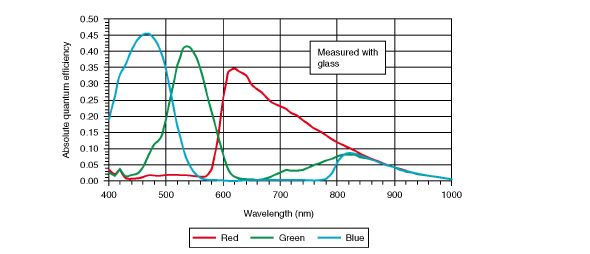
Figure 6.9 Colour quantum effciency with microlens for the Kodak KAI-4021 interline transfer CCD image sensor. The sensor is a 4 million pixel sensor with 7.4 um2 pixels with microlenses. Reprinted with permission from Eastman Kodak Company.
colour filter patterns offer higher sensitivity compared to the RGB primary colour filter patterns, but there is a deterioration in the signal-to-noise level under normal illumination conditions as a result of the conversion of the complementary colours to RGB signals.

Figure 6.10 A schematic diagram of the Bayer colour filter array.
Since the CFA allows only one colour to be measured at each photosite, the two missing colours must be estimated if a full colour image is to be obtained. The process of estimating the missing colours is known as ‘demosaicing’ or ‘colour filter interpolation’ and is done off the sensor after the analogue signal has been converted to a digital form. Several methods exist for estimating the remaining colours at each pixel position. The techniques used extract as much information from neighbouring pixels as possible. The simplest methods estimate the missing colour values by averaging colour values from neighbouring pixels. These will work satisfactorily in smooth regions of the image but are likely to fail in regions where there is detail and texture. More sophisticated methods are therefore employed. For example, a reasonable assumption is that the colours across an edge detected in the image are likely to be different, while those along an edge are likely to be similar. Neighbouring pixels that span across an edge in the image are therefore avoided. Another assumption is that the colour of objects in a scene is constant even if lighting conditions change. Abrupt changes in colour only occur at edge boundaries. Sudden and unnatural changes in colour are avoided and only gradual changes allowed. The hue-based method was common in early commercial camera systems but has since been replaced by more sophisticated methods. A poor demosaicing method usually results in colour aliasing (or moiré) artefacts in the output image. These are commonly observed around edge regions or areas with high levels of texture or detail.
The demosaicing process is, in most cases, conducted within the image-processing chain in the camera and the user is likely to have little or no control over the process. Most professional and many higher-end consumer digital cameras today are able to save ‘raw’ image data. Raw data is the set of digitized monochrome pixel values for the red, green and blue components of the image as recorded by the sensor. Additional metadata relating to the image processing normally conducted in the camera is also saved. Proprietary software usually provided by the camera manufacturer can be used to reconstruct the full colour image externally to the camera and usually on a desktop computer. You will have more control over the quality of the result if you work with the raw image data (see Chapter 8).
Microlenses – increasing the effective fill-factor
As mentioned earlier in this chapter the IT array for CCD-type sensors has a number of advantages over the FT array. This includes the ability to capture frames at a very high rate due to its fast electronic shutter. The CMOS architecture was shown to have several advantages over

Figure 6.11 A cross-sectional diagram of photositeswith microlenses in an interline transfer CCD. Light incident on the sensor at oblique angles can result in crosstalk with neighbouring pixels resulting in vignetting and a general loss of sensitivity by the sensor.
CCD-type arrays. Both these array types are widely used in consumer digital cameras today. One of the primary drawbacks with the IT CCD array and CMOS sensors is the relatively low fill factor due to the metal shielding and on-chip electronics. To compensate for this, manufacturers ft small microlenses (or lenslets) to the surface of each pixel. The lenses are formed by coating resin on to the surface of the colour filter layer. The resin is patterned and shaped into a dome by wafer baking. Figure 6.11 shows a cross-sectional diagram of an interline transfer CCD with a microlens array. The tiny lenses focus the incident light that would normally reach the non-light-sensitive areas of the pixel to the regions that are sensitive to light. In this way the effective fill factor is increased from about 30–50% to approximately 70%. The sensitivity of the pixel is improved but not its charge capacity. A drawback of using a microlens is that the pixel sensitivity becomes more dependent on the lens aperture, since the lens aperture affects the maximum angle with which light is incident on the sensor. Wide-angle lenses used at low f-numbers that are not specifically designed for use with digital cameras can result in light reaching the sensor at oblique angles. This results in a reduction in the effectiveness of the microlens, since some of the incident light strikes the light-shielded vertical CCDs. (Note – if light is reflected into the neighbouring photosites, it causes colour crosstalk.) This can result in vignetting (corner shading) and a general loss in sensitivity of the sensor. Another phenomenon that is caused by microlenses is ‘purple fringing’. This results from a form of chromatic aberration which occurs at the microlens level and is most noticeable at the edges of high-contrast objects. An example of purple fringing is shown in Figure 6.12. You can learn more about how to choose lenses for your digital camera in Chapter 3.
Anti-aliasing and infrared cut-off filters
When a scene is captured digitally any patterns or colours that did not exist in the original scene, but are present in the reproduced image, are generally referred to as ‘aliasing’ (see page 160). Highly repetitive patterns and colours with sharp transitions occur regularly in the real world – for example, detail in fabric, strands of hair, text and metallic objects. If the sensor array that samples the image data projected by the lens is not fine enough then some degree of aliasing will

Figure 6.12 An example showing ‘purple fringing’. This can result from ‘chromatic aberration’ occurring at the microlens level. © Hani Muammar
result when the digital image is reproduced in a form that is suitable for viewing or printing. In a Bayer array sensor system, aliasing colour artefacts can be enhanced or reduced by different demosaicing processes, but processes that reduce the aliasing usually also reduce the image sharpness. To minimize aliasing artefacts manufacturers of DSCs ft anti-aliasing filters in the camera. The filter is an optical device that fits in front of the sensor and behind the camera lens (see Figure 6.1). The filter band limits the image by lowering the contrast of the highest frequency patterns in the scene to match the capabilities of the sensor. Apart from minimizing aliasing and moiré patterns, a side effect of the anti-aliasing filter is that it introduces a slight degree of controlled blurring in the reproduced image. This is normally offset by sharpening the image. This is done in the camera signal processing, but you can apply additional sharpening when editing the image on your computer.
Silicon, as mentioned earlier, is sensitive to radiation with wavelengths in the infrared region as well as visible light. Manufacturers therefore ft infrared cut-off filters to minimize the possibility of colour contamination due to the infrared wavelengths in the final image. Some anti-aliasing filters have a built-in secondary IR coating which filters out more of the IR wavelengths reaching the sensor. Most digital cameras have anti-aliasing filters fitted, although there are exceptions. The Kodak Pro 14n DSLR camera was fitted with a 13.7 megapixel (effective) full-frame CMOS sensor. You can read more about the meaning of megapixel ratings in the next section. In the Pro 14n Kodak decided to leave out the anti-aliasing filter and as a result the images delivered by the camera were exceptionally sharp. However, artefacts such as colour aliasing are sometimes visible in areas of very high detail. Another camera which lacked
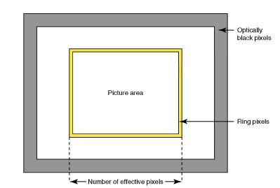
Figure 6.13 A schematic diagram showing pixels and their relationship to the image sensor.
an anti-aliasing filter was the Sigma SD-9 SLR. This camera was fitted with Foveon’s X3 sensor (see page 156).
Sensor size and pixel specifications
Probably the best known and widely reported sensor specification is the number of pixels of a digital still camera. This number, usually of the order of millions of pixels, relates to the number of photoelements, or pixels, that exists on the sensor itself. The number of pixels is usually associated with the quality and resolution of images that can be delivered by the digital camera. However, that is not always the case, and selection of a camera should not be based on pixel count alone. Several factors contribute to image quality, and some of these are discussed later in the section on sensor artefacts.
It is quite common that not all the pixels in a sensor are active when an image is captured. A proportion of pixels sometimes falls outside the image circle provided by the camera lens. ‘Ring’ pixels lie inside the image circle and are used for processing the captured image. They do not directly form part of the image itself. Some pixels that lie outside the ring area are optically black and are used for noise cleaning. You can read more about noise cleaning later in the chapter. Figure 6.13 is a diagram showing sensor pixels. Manufacturers of DSCs will report the number of ‘effective’ pixels as well as the number of ‘total’ pixels, particularly for higher-end DSLR cameras. The number of effective pixels is the total number of pixels that are used to create the image file, and includes the ring pixels described above. A guideline for noting camera specifications was published in 2001 by the Japan Camera Industries Association (JCIA). This guideline is now maintained by the Camera and Imaging Products Association (CIPA) after the JCIA was dissolved in 2002. (Note – A similar guideline, ANSI/I3A 7000, was published in the USA in 2004.) The guideline states that the effective pixels should not include optically black pixels or pixels used for vibration compensation. The effective number of pixels provides a more realistic indication of the image capture performance than the total number of pixels.
In Chapter 2 an overview of image sensor sizes was given. CCD sensors today are given a ‘type’ designation that has origins that date back to the standard sizes that were assigned to imaging tubes more than 50 years ago. The optical format types (for example, 0.5 in.) are historically based on the outer diameter of the glass envelope of a vidicon tube. Examples of sensor types and their respective diagonal lengths, in millimetres, can be found in Figure 2.5. An estimate of the approximate diagonal length of the sensor can be made if you assume that 1 in. equals 16 mm for optical sensors with formats that are greater than 0.5 in. For sensors with formats smaller than one-third of an inch assume that 1 in. equals 18 mm. Full-frame sensors have dimensions that correspond to the size of a 35 mm frame of film. They are normally used by professional digital SLR cameras. The Canon EOS-1Ds and the Kodak DSC-14n are examples of DSLRs that use a full-frame sensor. The Four Thirds standard was developed by Kodak and Olympus for use with DSLR camera systems. The system specifes the sensor format as well as lens specifications and is designed to meet the requirements of a fully digital camera system. One of those requirements is the telecentric lens design, which you can read more about in Chapter 3. The sensor size, referred to as a Four Thirds type sensor, has dimensions that are slightly smaller than other DSLR sensors but larger than compact digital camera sensors. One way that the Four Thirds system differs from the 35 mm film format is in its image aspect ratio. It uses a 4:3 image aspect ratio compared to the aspect ratio of 3:2 used by the 35 mm format. The 4:3 aspect ratio has traditionally been used by television and has become the most commonly used aspect ratio in computer monitor display standards. Some cameras that use the Four Thirds system include early designs such as the Olympus E-1, released in 2003, and more recently the Olympus E-510, released in 2007. Other manufacturers such as Panasonic, Fujifilm, Sanyo, Leica and Sigma have also developed cameras that use the Four Thirds system. In 2008 the Micro Four Thirds standard was announced by Olympus and Panasonic. The standard uses the same Four Thirds sensor but, unlike the Four Thirds system, Micro Four Thirds eliminates the requirement for a mirror and a pentaprism necessary for the through-the-lens viewfinder system in an SLR camera. This makes it possible for smaller, lighter camera bodies to be designed, together with more compact and lighter lenses. An electronic or optical viewfinder is required due to the absence of the mirror and prism mechanism. Lenses designed for DSLRs based on the Four Thirds system can be used with an adapter, but Micro Four Thirds lenses cannot be used on Four Thirds camera bodies. An example of a Micro Four Thirds camera is the Olympus PEN (see Figure 6.14).
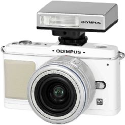
Figure 6.14 The Olympus E-P1 camera with FL-14 flash. The camera is based around the micro Four Thirds standard and is styled around the original Olympus Pen FT half-frame camera. Image courtesy of Olympus Cameras.
Alternative sensor technologies
In this section you will read about two different and alternative sensor technologies that are currently being used in commercially available digital cameras today. The Foveon sensor uses CMOS semiconductor technology but uses a three-layer photodetector that ‘sees’ colour in a way that mimics colour film. The Super CCD is based on CCD technology but uses an alternative pixel pattern layout that is based on a ‘honeycomb’ pattern. A new colour filter array layout that provides higher sensitivity to light due to the use of ‘panchromatic’ (monochrome) pixels is described. Backside illumination is a technology that has recently become more commonly available in consumer digital cameras. An overview of backside illumination is provided and a description of how an alternative arrangement of components in a sensor can improve its low light performance. Finally, you will read a brief introduction about the Live MOS, a new generation of sensor that can offer the high image quality of a CCD sensor with the low power consumption of a CMOS sensor.
The Foveon sensor – X3
The Foveon X3 image sensor, introduced in 2002 by Foveon Inc., is a photodetector that collects photoelectrons using three different wells embedded in the silicon. As described earlier in this chapter, image sensors are essentially monochrome-sensing devices, and by using an array of colour filters superimposed over the photodiodes a colour image from the scene can be obtained. Application of a CFA, such as the Bayer pattern, however, means that only one colour is detected per pixel and values for the other two colours need to be estimated. Unlike conventional sensors based on CFAs, the Foveon sensor is capable of capturing red, green and blue colours at each pixel in the array. The demosaicing process described for CFA-based sensors is not needed with the Foveon sensor.
The Foveon sensor is based on the principle that light with shorter wavelengths (in the region of 450 nm) is absorbed closer to the surface of the silicon than light with longer wavelengths (600–850 nm). By specially designing each photosite to collect the charge accumulated at different layers of the silicon, a record of the photon absorption at different wavelengths is obtained. Figure 6.15 shows a cross-sectional diagram that illustrates the sensor layers. The Foveon sensor is formed by stacking three collection wells vertically, thereby collecting photons at different depths. The silicon itself acts as a colour filter, since the blue photons are more likely to recombine near the upper well, while the red photons are more likely to penetrate much more deeply into the silicon and recombine near the deepest well. The spectral responses of the three wells are very broad, however, somewhat similar to cyan, magenta and yellow filters. Infrared and UV cut-off filters are used to band-limit the captured light. Although the demosaicing process is not needed, several processing steps and

Figure 6.15 A schematic cross-sectional diagram of a FoveonX3 sensor. Light with short wavelengths is absorbed near the surface of the silicon while longer wavelength light is absorbed deeper in the silicon.
image-processing functions are applied before the captured image data is suitable for being viewed on a colour monitor or printed. This includes colour correction processing to compensate for the overlapping spectral sensitivities of the three collection regions.
The Sigma SD9 digital SLR camera was the first camera to use the X3 Foveon sensor. It produced a 10.2 million value raw file that comprised 3.4 million values per colour channel. After processing the raw values a 3.4 megapixel image file was produced. It is generally recognized that images captured with the X3 sensor have higher resolution than those captured with a Bayer sensor when the detail in the scene comprises mainly red and blue primaries. The resolution provided by the X3 sensor was claimed to be comparable to a Bayer sensor with between 5 and 8 megapixels. However, the performance of the X3 sensor under low light conditions has been noted to produce noisier images.
The Super CCD sensor
The arrangement of photosites described earlier for CCD and CMOS sensors involved placing rectangular photosites on an x–y grid pattern. One of the problems with IT and CMOS designs was the relatively low fill factor due to the charge storage area in the vertical CCD. One arrangement that results in an increase of the active (light-sensitive) area in the pixel relative to the normal IT CCD is the pixel interleaved array CCD (PIACCD). (Note – this PIACCD is still an IT CCD.) The PIACCD, more commonly known as the Super CCD, was developed by Fujifilm in 1999. Octagonally shaped pixels are placed in a honeycomb pattern as shown in Figure 6.16. The arrangement increases sensitivity, since the photodetectors are slightly larger. The pixel pitch of the Super CCD is finer in the vertical and horizontal directions than is the case for a normal IT CCD with an equivalent number of pixels. This is achieved at an increase in pixel pitch along the diagonal axes (45° from the normal). The sampling characteristics of the Super CCD are reported to be better suited to the properties of the human visual system, which is more sensitive to vertical and horizontal patterns.
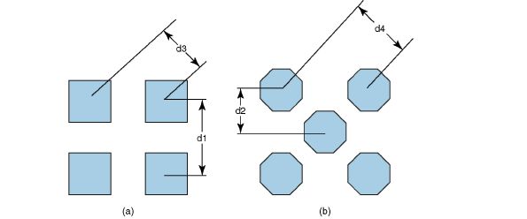
Figure 6.16 (a) Rectangular photosites on a conventional grid. (b) The Fuji Super CCD arrangement comprising octagonal sensors in a honeycomb arrangement. Note the vertical distance, d1, between cells in the conventional grid is larger than the inter-photosite distance, d2, in the Super CCD. The same applies to the horizontal distance. However, the spacing in the diagonal direction of the Super CCD, d4, is greater than the spacing in the conventional grid, d3.
To produce an image that can be manipulated, viewed on a monitor or printed, the information captured by the octagonal pixels in the Super CCD has to be first converted to a digital image with square pixels. This is done using a colour filter interpolation process that converts the offset colour sample values to an array of square pixel colour values. Since the introduction of the original Super CCD, Fujifilm has developed newer generations of the sensor known as Super CCD HR (high resolution) and Super CCD SR (super dynamic range). The SR sensor uses the same honeycomb pattern as the HR sensor. Each octagonal photodiode, however, is replaced by two smaller octagonal photodiodes that differ in size and hence sensitivity. They are known as the primary and secondary photodiodes, and are placed under the same microlens and colour filter. The primary photodiode, which is larger and hence more sensitive than the secondary photodiode, measures the majority of light from the scene. The secondary photodiode has low sensitivity and records only the brightest parts of the image. Because of limitations in the charge storage capacity of a photodetector, described earlier in this chapter, photons reaching the sensor from the brightest parts of the scene can result in overfow of charge. Detail present in the brightest part of the scene is not therefore always recorded by the primary photodiodes. Fuji claim that combining the output from the primary and secondary photodiodes produces an image that contains more detail in the highlight and dark areas of the image than is possible with a conventional CCD sensor. However, this combination occurs only after the separate samples have been read out from the sensor, which doubles the number of charge packets that must be transferred, compared to a conventional IT CCD.
Kodak Truesense high sensitivity sensor
The red, green and blue colour filters that form the Bayer pattern lower the overall sensitivity of the sensor to light compared to a sensor without any colour filter. This is due to the fact that each filter in the Bayer pattern has a spectral transmittance that attenuates the incoming light at frequencies that lie within the visible spectrum. The Bayer pattern is not ideally suited to low light imaging conditions, since fewer photons entering a photosite mean fewer electrons are generated, which can result in excessive noise artefacts in the final image. An alternative filter layout to the Bayer pattern which results in higher sensitivity to light is to add panchromatic (or ‘clear’) pixels to the colour filter array. Since the panchromatic pixels are sensitive to light at all the visible wavelengths, a higher proportion of light striking the sensor is collected. A number of filter patterns based on this concept were introduced by Eastman Kodak in 2007. In one arrangement, closely based on the Bayer pattern (see Figure 6.17), half the pixels on the sensor are panchromatic, a quarter are green, and the remaining pixels are equally divided between blue and red. The technology can be applied to sensors of any size and megapixel count, and works with both CCD and CMOS sensors. Kodak claim between one and two photographic stops improvement in sensitivity over the traditional Bayer pattern. The trade-off is in the resolution of the colour pixels, which is lower than the Bayer pattern. Special algorithms are used to combine the pixel data from the panchromatic pixels with the colour pixels to generate a full colour image. Kodak has deployed its Truesense colour filter pattern in both CCD and CMOS sensors for applications in the areas of high-resolution medium-format photography, HDTV video and mobile imaging.
Figure 6.17 In Kodak’s Truesense technology the traditional Bayer pattern is extended by adding panchromatic pixels to the existing red, green and blue pixels already in the filter pattern.
Back-illuminated sensor technology
Back-illuminated sensor technology is an alternative sensor design that has been in use for some time in specialist applications such as astronomy and low-light security systems. Due to the highly complex and expensive manufacturing process, the technology wasn’t applied to consumer photography until recently. In a conventional sensor, the matrix of electrical wiring and interconnections are deposited on top of the light-sensitive silicon during fabrication. When a scene is photographed, light from the camera lens is directed through the microlens and colour filter and has to pass through a ‘tunnel’ created by the metal interconnections until it reaches the photodetector. This technology is commonly known as front-side illumination (FSI) and has traditionally been used in CCD and CMOS sensors. The metal interconnects that create the ‘tunnel’ through which light passes can refect or absorb some of the incoming photons, thereby reducing the number of photons reaching the photodetector. As pixel dimensions continue to shrink, the amount of light reaching the photodetector continues to fall and the low-light performance and image quality is further degraded. In a back-illuminated sensor, the matrix of metal wiring and interconnects is moved to the back of the photosensitive silicon layer. Incoming light reaches the photodiode directly after passing through the microlens and colour filter, and is no longer required to pass through layers of metal interconnects (see Figure 6.18). OmniVision Technologies developed a back-illuminated CMOS sensor in 2007, although

Figure 6.18 Cross-sections of (traditional) front-illuminated and back-illuminated sensor structures.
its adoption was slow due to its high cost. In 2009 Sony introduced its own range of back-illuminated CMOS sensors called Exmoor-R and these have proved popular in several consumer digital cameras using this technology today. Back-illuminated sensors appear to offer advantages in low-light imaging compared to front-side illuminated sensors. However, disadvantages with back-illuminated sensors include crosstalk resulting from photons being collected by the wrong pixel and the expensive and complex manufacturing process.
The Live MOS image sensor
Traditionally, CCDs have provided the highest level of image quality at the expense of power consumption. CMOS imagers, on the other hand, have traded off image quality and cost for a higher level of system integration (functionality on-chip) and lower power dissipation. The dividing line between CCD and CMOS sensors today is less distinct. CCD sensors have become more power efficient and CMOS sensors are capable of delivering image quality that is comparable to CCDs. The Live MOS sensor technology has been used by Panasonic, Olympus and Leica in their digital camera systems since 2006. The technology claims to offer image quality equivalent to CCD-based systems with energy consumption levels close to those of CMOS technology.
Image artefacts associated with sensors
You will have read earlier about some of the limitations and constraints that exist in the design of image sensors. These constraints often give rise to some well-characterized image artefacts, which can affect the quality of the reproduced image. Probably the best known and widely discussed artefact is image noise. This is an apparently random variation in pixel values that is similar to the grain that is sometimes visible when enlargements are made from film. If image noise is excessive, it can be undesirable. On the other hand, noise may be introduced purposefully to add artistic value to an image. Other image artefacts include blooming, clipping, aliasing or moiré patterns and, in the case of DSLRs with interchangeable lenses, dust on the sensor. In this section you will read more about what causes these artefacts, how to recognize them and how to avoid them.
Aliasing and moiré
Patterns and textures in the real world can take on an infnite range of shapes and frequencies. When a digital image is acquired the scene is sampled at discrete spatial positions by the image sensor. If the highest frequency in the scene exceeds the sampling frequency of the image acquisition system, then aliasing can occur. Aliasing can give rise to jaggies or moiré patterns in the image. Moiré patterns are visible as a pattern of stripes or bands that exist where the level of texture and detail in the scene is high. Aliasing can occur not only at the acquisition stage of an image, but can be introduced when an image is resized to contain fewer pixels. To avoid aliasing it is necessary to band-limit the input data using a low-pass filter. The low-pass filter is carefully designed to limit the maximum frequency to a value that is less than the sampling frequency. As mentioned earlier in this chapter (page 152), most digital cameras today contain an optical anti-aliasing filter between the sensor and the camera lens to limit the range of input frequencies reaching the camera sensor. Anti-aliasing filters can, however, introduce some blurring into the reproduced image and manufacturers try and reach a compromise in the design of the filter. Coloured moiré patterns can also be introduced by the sampling and demosaicing processes in Bayer arrays. The effect here is observed as a pattern with false-coloured edges. Figure 6.19 is a photograph that clearly shows the effect of colour moiré.
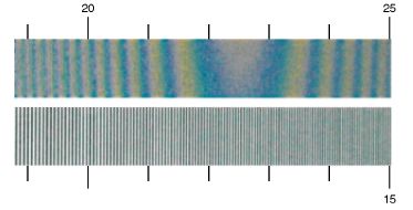
Figure 6.19 A photograph illustrating aliasing and colour moiré in a digital camera. The numbers relate to the width of the vertical bars and are defined as the number of lines × 100 per picture height. In this example, strong aliasing and colour moiré are seen between 2000 and 2500 line widths per picture height. This corresponded to a spacing of approximately 0.1 mm between the black vertical bars.
Special image charts containing swept black and white square-wave or sinusoidal patterns can be used to probe aliasing in digital cameras. One such target, the circular zone plate, is a chart containing a two-dimensional swept (continuously varying spatial frequency) sinusoidal wave. This chart is essential when it comes to designing the anti-aliasing filter in a DSC. The ISO 12233 standard test chart was developed for the purpose of testing digital still cameras and is described in more detail in Chapter 3. The chart contains swept square-wave patterns which can be used to explore the amount of aliasing introduced by the camera. The ISO test chart is shown in Figure 3.21. When evaluating digital cameras look for colour moiré artefacts in high-frequency and textured patterns. If possible look at a digital image of a test chart containing fine detail (such as the test chart described above) captured with the camera you are evaluating.
Blooming and clipping
The range of lightness values encountered in a typical scene is very wide and levels can often exceed 10 photographic stops when refections from diffuse and specular objects and light sources such as the sun are taken into account. When a high level of light is incident on a photodiode in an image sensor, the well capacity of the photodiode may be exceeded. Charge may then leak into neighbouring pixels and blooming can occur. This is usually seen as a bright area around the bright spot in the image where charge overfow occurred. Sources that can give rise to blooming include the sun, a specular refection off a metal object or a lit candle captured under low light. In CCD sensors, a characteristic vertical streak that extends along the height of the sensor can occur. This happens when charge leaks into the vertical charge transfer array and contributes to the charge being transferred out of the sensor. Figure 6.20 shows an example of blooming. Note that blooming can increase the visibility of purple fringing described earlier in this chapter.
Normally when a scene is captured using a digital camera, the camera electronics will attempt to expose for the most important parts of the scene, usually the midtones. If the tonal range in the scene is very high – for example, a bright sunny day – or a powerful flash was used to light the subject, small changes in lightness at either end of the lightness scale may be impossible to discriminate in the resulting image. In this case the pixel values in the image are constrained

Figure 6.20 An example showing the effect of blooming in a digital camera image. © Hani Muammar
(clipped) to the maximum value, at the scene highlights, or minimum value, at the scene shadows. The maximum and minimum values are set by the output device capabilities or image file format. Figure 6.21 shows an image containing highlight clipping. Note the regions in the image where detail is lost. Clipping can occur in one or more of the red, green or blue pixel values of the output image. If highlight clipping occurs in one or two colours, then a colour shift is frequently seen. For example, if the red pixels are clipped, Caucasian skin can turn orange–yellow in hue. Some quantization (banding) may also be observed. If all three colours are clipped then detail is completely lost and the area becomes white. Scene highlights are said to be burnt out. With shadow clipping, detail may be lost and shadow pixels can take on a coloured appearance, although shadow clipping is generally less noticeable and objectionable than highlight clipping. The best way to avoid clipping is to underexpose the image slightly. You can adjust the lightness and contrast of the image manually later on your computer.
Image noise
One of the aspects of digital cameras that has attracted much interest over the years is image noise. Noise in digital images appears as a random variation in pixel values throughout the image. It is often described as the equivalent to grain in silver halide film. Although noise can take on the appearance of grain in a print or slide, it can be more objectionable when it appears as a low-frequency mottle or if it is combined with colour artefacts. Figure 6.22 shows an example that illustrates the appearance of noise in digital camera images. In general, the sources in a digital camera that contribute to image noise are difficult to identify. It is certain, however, that there are several sources of noise and they all appear as variations in image intensity. The sources of noise fall broadly into two categories: fixed pattern noise (FPN) and temporal noise.

Figure 6.21 A photograph showing an example of highlight clipping. Note the dramatic shift in hue that occurs in the sky region. The blue pixels are the first to clip, followed by blue and green and finally all three colours. © Hani Muammar
Fixed pattern noise
Fixed pattern noise (FPN), as the name suggests, is image noise that forms a spatially fixed pattern across the image. Most of the FPN noise is introduced under dark conditions, for example if the lens cap is on or the subject is not illuminated. The source of the noise is mainly due to dark current non-uniformity (DCNU) and results when the dark current of each pixel is different over the sensor array. Dark current is the small amount of electrical current that continues to fow through the device even though no photons are reaching it. Because the generation of dark current is a random process, it is possible to reduce the noise caused by DCNU, but not to eliminate it, by subtracting the average dark current of each pixel from the captured image (see page 149). Some FPN is also introduced under illuminated conditions. DCNU is generally not visible under normal illumination conditions but can often be observed when exposure times are long – for example, in low-light photography. High temperatures increase DCNU, and sensors used in astrophotography are frequently cooled to reduce the level of DCNU. Dark current can also reduce the available dynamic range of the sensor, because the well capacity of the pixel is reduced. The dynamic range of a sensor is the ratio of the maximum output signal that can be obtained from the sensor to the dark noise output signal level.

Figure 6.22 A photograph showing the effect of noise in a digital camera image. © Hani Muammar
Temporal noise
Temporal noise is a variation in image noise from one image to the next. Pixel values vary randomly over time. Unlike FPN, temporal noise can be removed by averaging the frames taken from several exposures. The effect of noise reduction by frame averaging is a characteristic of the human visual system. When you go to the movies or watch television, your eye naturally smoothes out most of the noise in the picture by averaging it from frame to frame. Some of the sources that contribute to temporal noise include shot noise, reset noise, read noise and dark current shot noise. The quantifcation of the effect of noise in an image on the performance of an imaging system is reported by measuring the signal-to-noise ratio (SNR). High values of SNR correspond to high signal quality and relatively low noise level. When the ratio of signal to noise is low, image quality can degrade and noise is likely to be more visible in the image.
Shot noise
In any photodetector system where photons arrive randomly and are converted to charge, the resulting noise is associated with shot noise. For example, shot noise is observed in thermionic values (or vacuum tubes) and semiconductor devices such as photodiodes and MOS transistors. During exposure of a photodetector to light, the actual number of photons that are collected by the detector is not known. What is known is the average number of photons collected. Therefore, the actual number is described by a statistical distribution, known as the Poisson distribution, whose mean is centred at the average number of photons collected. In this distribution the standard deviation (a measure of the spread of values) is equal to the square root of the average number of photons. The SNR is then found by dividing the average number of photons collected by the standard deviation of the noise. The best possible SNR that can be achieved by a detector is the square root of the average number of photons collected. Shot noise is more problematic at low light levels since the SNR is low. At high light intensities the SNR is higher and shot noise has a negligible effect.
Reset noise
Another source of noise is reset noise. At the sensor device level, before charge is converted into a voltage, the photodiode and video line circuitry are reset to a reference voltage by a field effect transistor (FET) amplifer. There is an uncertainty in the reference voltage that arises due to the interaction between the FET and the capacitance of the photodiode and amplifer circuitry. This noise is dependent on temperature as well as capacitance. Most manufacturers of image sensors are able to eliminate reset noise completely using special signal processing circuitry.
Read noise
Read noise (also known as readout noise or output amplifer noise) is noise that is added to the charge when it is read out of the sensor. This noise is independent of the exposure time and is produced when the charge is converted from an analogue to a digital value. Thermally dependent noise is present in the output amplifer and contributes to read noise. Other sources of read noise include flicker noise and clocking noise. Flicker noise is a noise that is inversely dependent on the frequency with which pixels on the sensor are read. Cameras that read out pixels slowly have higher flicker noise. Clocking noise arises from the various clock circuits that are used in the camera electronics to transfer the image through the sensor and to eventually process the data. Variability in the clock edge due to jitter contributes to clocking noise. Higher clock frequencies introduce high levels of clocking noise into the system.
Dark current shot noise
Dark current noise was discussed earlier in the context of FPN. Although average dark current noise that contributes to FPN can largely be eliminated, the shot noise component of dark current cannot be reliably removed. The shot noise associated with dark current is also equal to the square root of the average integrated dark charge at the photosite.
The influence of sensor size on noise
Most image sensors used in compact DSCs are very small. In Figure 2.5 you can see that the typical size of a sensor fitted in a compact DSC is in the region of 6.7–16 mm when measured diagonally. Compared with the size of the sensors fitted to many DSLRs (around 28 mm), these sensors are very small. Today the numbers of pixels offered on compact DSCs and DSLRs are very similar and many cameras offer pixel counts in the region of 10–12 megapixels. Thus, the dimensions of photosites in sensors fitted to compact DSCs are significantly smaller than those fitted to DSLRs. The current state-of-the-art pixel size is of the order 2.2 µm for CCD sensors and 2.25 µm for CMOS sensors. Very recently image sensors with 1.75 and 1.4 µm pixel sizes have been announced. By comparison the pixel size in a Nikon D70s SLR, which is fitted with a 23.7 mm × 15.6 mm, 6.1 megapixel sensor array is 7.8 µm. Smaller pixel sizes result in a decrease in sensitivity and full-well capacity. Smaller pixels are therefore less effective at accumulating charge from incident photons and for a given exposure, the amount of amplification needed is higher. Increasing the level of amplification also increases the noise. Thus, under low light conditions, smaller sensors are more likely to produce noisier images than larger sensors. The reduction in full-well capacity also means that the dynamic range is likely to be reduced. Photosites are likely to reach saturation more quickly, thereby resulting in clipping or blooming in the output image. The resolving capability of small pixels is also affected (see Chapter 2 for more information about pixel size and resolution).
It is worthwhile noting, however, that under high levels of illumination sensors with low sensitivity produce perfectly good images with very low levels of noise. Under these conditions, the cameras are likely to be used at their lowest ISO settings (for example, 80 or 100 ISO) and the signal amplification from the sensor will be at its minimum. It is under low illumination levels, when the ISO setting in the camera is likely to be set higher (for example, 400 or 800 ISO) that noise in the image can become problematic.
Reducing noise
Most digital cameras employ some form of internal processing that reduces the level of noise in the image. You can also reduce noise in your images after you have transferred them to your computer using special image-editing software that offers a noise reduction capability. High levels of noise are more difficult to remove, especially if the noise is combined with colour artefacts. In this case noise reduction algorithms are sometimes unable to distinguish between the noise and fine detail in the image. Sometimes it is preferable to leave some noise in the image rather than to apply large levels of noise reduction which can result in the loss of fine detail.
Defective pixels
Hot pixels are created by pixels on the sensor that have a higher rate of dark current leakage than other neighbouring pixels. As mentioned earlier, all pixels have some degree of current leakage which is visible as FPN under long exposures. Hot pixels are simply pixels with significantly higher than average dark current leakage. They normally are visible as bright one pixel wide spots that may be coloured red, orange, green, yellow or just appear as white pixels. Hot pixels are more likely to be noticeable when illumination levels are low and exposures are long. They may become more apparent after the camera heats up during a prolonged period of usage. Other pixel defects include ‘stuck’ pixels and ‘dead’ pixels. Stuck pixels are pixel values that take on the maximum value independent of the exposure level. In Bayer sensors they will appear as either red, green or blue pixels depending on the colour of the Bayer filter tile that overlies the photosite. Dead pixels are pixels that read the minimum value (zero or black) and are also unaffected by exposure. All these types of pixel defects can usually be masked by image processing that is done internally in the camera, which replaces the defective pixel value with the average of neighbouring pixels of the same colour.
Dust
A problem that can affect digital cameras is when dust or other materials, such as moisture, are unintentionally deposited on the surface of the sensor. This is more common with DSLR cameras with interchangeable lenses. Every time the lens is removed dust can enter the camera body through the lens opening. When the camera is switched on dust may adhere to the sensor surface. One possibility is that a static charge builds up on the sensor and may attract the dust. The effects of dust are most apparent when photographs are taken with very small apertures due to the large depth of focus. They are least apparent at large apertures. Usually sensor dust can appear as dark specs in a uniform region, such as a blue sky. One of the problems with dust is that it is cumulative and can get worse over time. Many alternatives exist to reduce the effects of dust on the sensor. You can remove the effects by using appropriate image-editing software on your computer, or you can send the camera back to the manufacturer for cleaning. Other options include cleaning the sensor yourself using a hand blower bulb. Note that compressed air is not recommended because it is too forceful and may contain a liquid propellant. or brushing the sensor using a special brush with very fine fibres. Recently manufacturers of DSLR cameras have built integrated dust removal systems into their cameras. The Canon 400D camera removes dust using ultrasound vibration, a procedure that takes about one second to complete.
SUMMARY
- One of the basic building blocks of a CCD sensor is the MOS capacitor. When light is absorbed in a semiconductor a conversion from photon to electrical charge takes place. The amount of charge that is collected by a photodetector is proportional to the amount of light received over a given period of time. This is known as the integration time.
- Frame transfer arrays and full-frame arrays are commonly used CCD architectures in DSLR cameras. Frame transfer arrays contain a light-sensitive array of photosites and a metal-shielded charge storage area that is used to temporarily store the charge before it is transferred off the sensor. Full-frame arrays are simpler to manufacture and reduce smear during charge transfer by eliminating the storage array.
- Interline transfer arrays are the most common type of CCD array in consumer digital cameras today. Each pixel comprises a photodiode and an associated light-shielded charge storage area. A benefit of interline transfer arrays is their ability to capture video. Their main disadvantage is that fill factor is reduced. This can be offset by using microlenses.
- APS technology in CMOS sensors enables both the photodiode and readout amplifer to be incorporated into a single photosite. Charge accumulated is converted to an analogue voltage in the photosite and can be converted to a digital signal by on-chip analogue-to-digital (A/D) converters. Advantages of CMOS arrays over CCD arrays include higher on-chip system component integration, lower power supply requirements and the capability to read out windows of interest.
- Optically black photosites (also known as dummy pixels) are photosites on the sensor that are covered by a metallic light shield that prevents light from reaching the light-sensitive components during exposure. They play an essential role in determining the black reference level for the image sensor output.
- CFAs enable the separation of light incident on the sensor into three colour channels. This is performed on the sensor by covering each photosite with a colour filter corresponding to a single colour. The most popular arrangement of colour filters is the Bayer pattern array in which light is separated into red, green and blue components. A demosaicing process is applied to estimate the missing colours at each pixel, thereby enabling a full colour image to be generated.
- Microlenses are used to increase the effective fill factor of CCD interline transfer arrays and CMOS arrays. A drawback of using microlenses is that pixel sensitivity is more dependent on the lens aperture and the angle at which light is incident on the sensor.
- Anti-aliasing filters are normally fitted to reduce the possibility of aliasing or colour moiré in the final digitized image. Infrared cut-off filters are normally fitted to reduce the possibility of colour contamination due to infrared wavelengths in the digitized image.
- The ‘effective’ number of pixels in a digital camera is the total number of pixels that are used to create the digital image file, but should not include optically black pixels or pixels used for vibration compensation. The special requirements of digital cameras have prompted the development of entirely digital systems that specify the sensor used to the design of lenses which are tailored to the requirements of the sensor.
- The Foveon X3 sensor uses three vertically stacked photodiode array wells that collect electrons at three different depths in the silicon. Because the Foveon sensor captures all three colours at each pixel position it can provide higher resolution than Bayer sensors having the same number of pixels. The Super CCD sensor is an arrangement of octagonally shaped photosites in a honeycomb pattern. Sensitivity and vertical and horizontal resolution are increased relative to conventional CCD arrays.
- In a back-illuminated sensor the metal wiring and interconnections are placed at the back of the photosensitive silicon layer. The need for light to pass though the ‘tunnel’ of interconnects is eliminated. This improves the low-light performance capability of the image sensor, compared to front-illuminated sensors, because incoming light reaches the photodiode directly after passing through the microlens and colour filter.
- Jaggies or moiré-type patterns can be introduced into an image as a result of aliasing. Coloured moiré patterns may be introduced by the sampling and demosaicing processes in Bayer-type sensors. Special test charts containing fine detail can be used to evaluate the degree of aliasing in a digital camera.
- Blooming is seen as a bright area that is roughly centred about a bright spot in the image. It results when charge overfow in the sensor occurs. Clipping is when one or more of the colour bands in a digital image reach their maximum or minimum value. It can occur in the highlight or shadow regions of an image, resulting in loss of detail.
- Sources of noise in a sensor include FPN and temporal noise. DCNU is problematic under low illumination conditions and can be significantly reduced using processing. Sources of temporal noise are shot noise, reset noise, read noise and dark current shot noise. Temporal noise is more difficult to remove in a camera because it varies between exposures.
- The small sensor sizes used in compact DSCs are less effective at accumulating charge from incident photons for a given exposure and pixel count than the larger sensors used in DSLRs. This is due to the smaller pixel dimensions. It is difficult to remove large amounts of noise without affecting fine detail in the image.
- Defective pixels in a sensor include hot pixels, stuck pixels and dead pixels. Hot and stuck pixels are frequently visible as bright pixel-wide spots in the image. Dust on the sensor is a problem that can affect DSLR cameras with interchangeable lenses. Dust on the sensor can appear as specs of dark pixels and are more visible in large uniform regions of the image.
PROJECTS
1 In this project you will take an exposure in the dark using your digital camera. This will allow you to observe the effect of noise due to DCNU in the image sensor of your digital camera. This noise forms most of the FPN that is present in the sensor. You will also be able to see if your camera has any hot pixels. Preferably use a camera with manual ISO speed and exposure controls. Disable the flash and set the ISO control to ISO 100 or 200. Turn off any long exposure noise reduction and set the image quality to normal or fine. Set the capture image size in the camera to large and preferably minimize any in-camera image sharpening. Set the white balance to daylight. Then set the exposure mode to manual or shutter priority, place the lens cap on the camera lens and in a darkened room take several exposures with an exposure time of about 8 seconds. Transfer your images to your computer and open them up using an image-editing software package such as Adobe Photoshop. Boost the pixel values in the image using the ‘Levels’ command in Photoshop or an equivalent tool until the noise pixels are visible. Look for hot pixels in the image and note the similarity in noise patterns between the different frames. You may have to zoom out so that a complete frame is visible.
2 To observe the effect of temporal noise, you can capture several frames under medium or low levels of illumination. Disable the flash and set the ISO value of your camera to ISO 400 or 800. Place the camera on a tripod and capture several exposures indoors at a normal exposure setting. Adjust the ISO setting, aperture and shutter speed as necessary. You can illuminate your subject using natural light from a window or using artificial illumination such as tungsten lighting. Do not move your camera between exposures. Transfer your images to your computer and compare the noise patterns in similar regions of the scene. Note the random nature of the noise and observe the low level of correlation between successive frames.
3 In this project you will observe the effect of blooming and clipping in a digital image. To demonstrate the effect of blooming, first disable the flash on your digital camera and set the ISO to ISO 200 or 400. Then capture an image of a bright light source – for example, an illuminated car headlamp at night or the fame of a burning candle in a darkened room. Note the effect of blooming around the light source. Demonstrate the effect of clipping by capturing a scene outdoors under brightly lit conditions. Underexpose the scene by about one stop so that no clipping is present in the image. Gradually increase the exposure until clipping in the highlight regions of the exposed image can be seen. Usually bright surfaces, sky and clouds will clip first. If the scene is too overexposed, large regions of the image will lose detail and colour.