
8
Systems Design: Digital and Analog Interfacing Methods
Chapter Outline
- Study interfacing circuits of keys with the MCUs
- Learn interfacing circuits with physical devices as follows : LEDs, LCD, touch screen, printer, motors, coils, sensors, displacement and rotation encoders
- Know how an MCU drives the lOs at large voltages and currents.
- Know how an MCU is used in the robots, instruments and control systems using the appropriately designed interfaces for a system
8.1 INTERFACING OF THE KEY (SWITCH), KEYPAD AND KEYBOARD
8.1.1 A Single Key (switch) and Its Interface
A key (switch) switch interfaces with the port using two signals. One signal is called scan (strobe). Second is called return (sense). Scan and sense signals are between the key and port.
Figure 8.1(a) shows a single key (push-button switch). The pins connect to Vcc (+5 V) through the appropriate resistances. This is done because the port in 8051 MCU is open drain.
A key is between the input and output pins. Scan signal is from pin of output port and the return signal (sensing signal) is to pin of input port. Both signals are initially in pulled state. They connect to Vcc (+5 V) through the appropriate resistances. State 1 means the connected transistor at port pin is in high impedance (off) state. Initial conditions of both signals are 1s.
When the scan signal is written as 0 (by writing 0 to the port by MCU instruction), the return signal when key is open (ends of key not in contact) will show input = 1. When the key is closed (is in contact due to pressing or touching of the key) the return signal will show = 0. The reason for it is as follows:
When 0 is sent on scan-signal, it means making the output stage transistor at port pin in conducting state (low-impedance state) at the output port pin. Therefore, input port pin at the return signal will sense 0 when the key is in contact because the input pin will get shorted through the conducting state transistor at the scan signal. The return signal thus senses the 0 of the scan signal and activates to 0 when the key is in contact (pressed or touched), else it remains at 1 (not pressed or touched).
8.1.2 Bounces in a Key (switch)
A key is a mechanical system with a spring. When the key is touched, pressed and released, the spring bounces back and forth. The return signal thus senses the 0 and 1 repeatedly due to the bouncing of the contact back and forth. The bounce is natural action of any spring. The sensed bit on the return signal at input port will also reflect that bounce.
Figure 8.1(b) shows the bounces in the sense state of the key. Note that the bouncing intervals decrease with time and after some time the bounce will become 0. The effects of the bounces back and forth must be suppressed. The bouncing period is typically between 2 ms and 10 ms. After 10 ms, the contact between ends stabilizes and bounces die down.
8.1.3 Removing Bounce Effects on Input State from Key Using Hardware
The meaning of debouncing is removing effects of the bounces. (No variations at the sensed state).
Assume that 10 ms is the minimum period up to which the key must remain in contact after the key bounces die down so that its state can be acceptable by the MCU (or a controller circuit). A Schmitt trigger (ST) circuit can be used for debouncing. The effects of bouncing are suppressed when reading the logic state at the sense signal when the circuit is connected to the appropriate resistance R and capacitance C. The R and C pair at ST is adjusted to get a time constant = 10 ms.
A latch circuit can also be used to remove the effects of bouncing. Figure 8.1(c) shows the Schmitt trigger and latch circuits, one of which can be used for debouncing. An IC MAX 690 can also be used in place of the Schmitt trigger circuit.
8.1.4 Array (Row) of Keys and Its Interface
An array of keys is required for inputs of different commands. A single scan signal can be used to scan an array or row of 4 or 7 keys. One end of each key connects to the scan signal. Other end of each connects separate lines for the return sense signals.
Figure 8.2 shows an array of four keys with one scan and four return signals for 4 sense signals. It shows an array of 4 keys with one scan S0 at P1.0 and four return signals R0, R1, R2 and R3 at P1.4, P1.5, P1.6 and P1.7. A key (switch) interfaces with the port pin using one scan signal and 4 or more return port pins for the sense signals.
Each port pin connects to Vcc (+5 V) through the appropriate resistance for scan and sense signals. [This is because the port in MCU is an open drain port.]
When 0 is sent at S0, it means making the output stage transistor at port pin in the conducting state (low-impedance state) at the output port pin. Therefore, the input port pin at are corresponding return signal R0 or R1 or R2 or R3 will sense 0 when the key is in contact because the input pin will get shorted through the conducting state transistor at the scan signal. The corresponding return signal thus senses the 0 of scan signal and activates to 0 when the corresponding key is in contact (pressed or touched), else it remains at 1 (not pressed or touched).
Assume that single scan signal S0 is from an output port pin P1.0 and four return signals (sensing signals) R0 to R3 from four ends of four keys connected to four input port pins P1.4 to P1.7.
Keys 0,1,2 and 3
If key 0 is in the pressed state then P1.4 =0, if key 1 is in the pressed state then P1.5 =0, if key 2 is in the pressed state then P1.6 = 0 and if key 3 is in the pressed state then P1.7 =0.
Figure 8.1 (a) Single Key (Push-button Switch) with Two Signals, One for Scan and Second for Return; (b) Bounce in the Input from the Key and (c) Debouncing Circuit Using Schmitt Trigger (Upper Circuit) or Latch Circuit (lower circuit), one of which is used for Debouncing

Figure 8.2 Array of 4 Keys with One Scan S0 at P1.0 and Four Return Signals R0, R1, R2 and R3 at P1.4, P1.5, P1.6 and P1.7
Therefore, Port P1 will have 1110 1110 (= EEH) if S0 is sent as scan and R0 (=0) activates, P1 will be = 1101 1110 (= DEH) if S0 is sent as scan and R1(=0) activates, = 1011 1110 (= BEH) if S0 is sent as scan and R2 is activate(=0) and = 0111 1110 (= 7EH) if S0 is sent as scan and R3 is activate(=0).
Hardware and Software Debouncing
A Schmitt trigger or latch circuit (Fig. 8.1(c)) each can be used to suppress the bounce at each key. Software debouncing is described in Section 8.2.
8.1.5 Keypad (Matrix of Keys) and Its Interfacing
A keypad can have 16-keys or 20 keys. It can perform sophisticated functions. Each key (switch) interfaces with port using one of the scan signal and one return sense signals. A set of scan signals can scan the number of arrays or rows of 4 or 7 keys if one end of each key connects each scan signal and other end of each connects separate return sense signals for each scan signal.
Sixteen keys are sensed with 4 scan signals and 4 return sense signals. Figure 8.3 shows four arrays of four keys each array with one scan and four return signals. Four scan signals for four arrays are S0 to S3 at P1.0 to P1.3. Four return signals are R0, R1, R2 and R3 at P1.4, P1.5, P1.6 and P1.7,respectively.
Key 0 to Key 3: Assume that single scan signal S0 is from an output port pin P1.0 and four return signals (sensing signals) R0 to R3 from four ends of four keys connected to four input port pins P1.4 to P1.7. If key 0 is in pressed state then P1.4 =0, if key 1 is in pressed state then P1.5 =0, if key 2 is in pressed state then P1.6 =0 and if key 3 is in pressed state then P1.6 =0.
- The port P1 will read 1110 1110 (=EEH) if S0 is sent as scan and R0 (=0) activates, P1 will be read = 11011110 (=DEH) if S0 is sent as scan and R1(=0) activates, = 10111110 (=BEH) if S0 is sent as scan and R2 is activate(=0) and = 0111 1110 (=7EH) if S0 is sent as scan and R3 is activate(=0).
Key 4 to Key 7: Assume that second scan signal S1 is from an output port pin P1.1 and four return signals (sensing signals) R0 to R3 from four ends of four keys connected to four input port pins P1.4 to P1.7.
Figure 8.3 Keypad for 16 Keys with P1.0-P1.3 (S0-S3) Scan Signals and P1.4-P1.7 (R0-R3) Return Signals
If key 4 is in pressed state then P1.4 =0, if key 5 is in pressed state then P1.5 =0, if key 6 is in pressed state then P1.6 =0 and if key 7 is in pressed state then P1.6 =0.
- Therefore, the port P1 will read 1110 1101 (=EDH) if S1 is sent as scan and R0 (=0) activates, P1 will be read = 1101 1101 (=DDH) if S1 is sent as scan and R1(=0) activates, = 1011 1101 (=BDH) if S1 is sent as scan and R2 is activate(=0) and = 0111 1101 (=7DH) if S1 is sent as scan and R3 is activate(=0).
Key 8 to Key 11: Assume that third scan signal S3 is from an output port pin P1.2 and four return signals (sensing signals) R0 to R3 from four ends of four keys connected to four input port pins P1.4 to P1.7. If key 8 is in pressed state then P1.4 =0, if key 9 is in pressed state then P1.5 =0, if key 10 is in pressed state then P1.6 =0 and if key 11 is in pressed state then P1.6 =0.
- Port P1 will read 11101011 (=EBH) if S2 is sent as scan and R0 (=0) activates, P1 will be read = 11011011 (=DBH) if S2 is sent as scan and R1(=0) activates, = 10111011 (=BBH) if S2 is sent as scan and R2 is activate (=0) and = 0111 1011 (=7BH) if S2 is sent as scan and R3 is activate (=0).
Key 12 to Key 15: Assume that the fourth scan signal S3 is from an output port pin P1.3 and four return signals (sensing signals) R0 to R3 from four ends of four keys connected to four input port pins P1.4 to P1.7. If key 12 is in pressed state then P1.4 =0, if key 13 is in pressed state then P1.5 =0, if key 14 is in pressed state then P1.6 =0 and if key 15 is in pressed state then P1.6 =0.
- Port P1 will read 11100111 (=E7H) if S3 is sent as scan and R0 (=0) activates, P1 will be read = 11010111 (=D7H) if S3 is sent as scan and R1(=0) activates, = 10110111 (=B7H) if S3 is sent as scan and R2 is activate (=0) and = 0111 0111 (=77H)if S3 is sent as scan and R3 is activate (=0).
Sixteen Keys Keypad: A keypad of 16 or 20 keys can be used as follows:
Example 8.1
Use of a 16-key pad is as follows: A telephone instrument consists of 16 keys. Ten keys are 0 to 9 for dialling a number. Two keys are * and # for some commands. Four keys are for up, down, left and right shift of the cursor on the display screen.
Example 8.2
A mobile phone has 16 keys plus a menu key. 16 keys are used for 16 distinct contacts. Menu key can be pressed on four sides (up, down, left and right) to connect the four distinct contacts. 20 signals from keypad are the most important part for multiple functions and human-computer interactions in mobile.
8.1.6 Keyboard and Its Interfacing
A 102- or 105-keyboard finds use in all computer systems. There several scan signals (arranged as rows) and several return signals (arranged as columns) in a keyboard.
Figure 8.4 shows a simple interface and internal circuit for a keyboard interface. There are 64 keys, which are connected to 8 scan signals S0 to S7 and eight return signals R0 to R7. When an decoder is used, the required number of port pins reduces to 3 for scan signals and another encoder reduces the required number of port pins to another 3 for return signals when there are 64 keys. A keyboard interface uses two encoder-decoder pairs each for scan signals and return signals. This is because there is large number of keys more than 16 when compared to the number of port pins.
An encoder circuit between 16 return signals and the port pins can reduce the port input pins requirement to 4. A decoder circuit between 16 scan signals and the port pins can reduce the port output pins requirement to 4 in place of 16. Keyboard-controlled circuit provides this pair.
Shift and CTRL Keys in the Keyboard Controller: Keyboard controller provides for two keys one for control and another for shift in addition to 64 keys.
8.1.7 Keyboard Controller
Keyboard uses a keyboard controller for interfacing. Figure 8.5 shows a keyboard controller circuit. It has the following subunits.
(1) Scan clock and counter output for scanning the keys using a keyboard controller: There is a scan clock. Assume that it can be used to give clock inputs to a 3-bit counter, which generates three outputs S′0, S′1 and S′2 counter when it counts from 0 to 7. The counter output is in encoded form for the scan signals S0 to S7. The counter output can be sent as keyboard eight scan signals S0 to S7 using a decoder circuit. Using the scan clock and counter the encoded scan bits are incremented from 000 to 111 in eight clock inputs.
(2) Decoder in the keyboard controller for scan encoded inputs: The scan signals encoding means there can be encoding of 8 scan signals by 3 signals (bits). The encoded output from 3 count pins connects to a decoder, then the decoder makes one of the signal among S0 to S7 = 0, remaining = 1s. Figure 8.4 shows the encoded inputs S′0, S′1 and S′3 and decoder output S0 to S7.

Figure 8.4 Encoder-decoder Pair when Interfacing the Large Number of Keys (= 64 + CTRL key + shift key) and the Number of Input and Output Pins = 8
- The count output = 000 means activate scan signal S0.
- Equal to = 001 on next clock pulse that means activate scan signal S1 and so on.
- = 111 then means activate scan signal S7.
(3) Encoder in the keyboard controller for return encoded outputs: The return signals R0 to R7 can be encoded to 3 output signals (bits) R′0, R′1 and R′2. The encoded output from 8 output pins connects to an encoder, then the encoder makes for one of the signals among R0 to R7 = 0, remaining = 1s. Figure 8.5 shows the encoded inputs R0 to R7 and encoder output R′0, R′1 and R′3.
- The encoded output = 000 means activate scan signal R0.
- Equal to = 001 means activate return signal R1 and so on.
- = 111 then means activate scan signal R7.
(4) Debouncing when using the keyboard controller: A debouncing circuit (hardware) [Fig. 8.1(c)] is required at each return signal, R0-R7. The keyboard controller provides for hardware debouncing of each key.
(5) ASCII coded output using the keyboard controller: ASCII 7-bit code is an international standard for numerals and letters. ASCII coding format for a keypad or keyboard is preferred. A byte is sent to serial port for each key in its ASCII code. Character 0 is sent to serial port as 48d (30H), 1 as 31H, A as 41H and B as 42H. Space key is sent to serial port as 20H.
Software routine is used to read the states of the keys and can convert the state of the pressed key to the ASCII code. Keyboard controller can also be used for this conversion. The ASCII code key in the keyboard controller is generated as follows: A ROM memory in the controller can be given the address bus inputs from S′0 to S′3, R′0 to R′3, and CTRL, SHIFT, ALT and other keys. The ASCII-coded byte is generated in the output ROM at data bus pins. Each output corresponds to the pressed single key or simultaneously pressed set of keys.
(6) Serial output: The data bus output of ASCII encoding ROM is sent to a UART circuit for converting the byte into UART format for sending it to serial port. Serial UART formatted output at a selected baud rate is generated by keyboard controller. Hardware sends ASCII code byte for a key on a serial signal with a predefined baud rate (for example, 1200 baud per s). The input to the MCU is on the RxD pin.
(7) Two-key lockout: Figure 8.6 shows how to prevent mistake of simultaneously pressing two neighbouring keys, a diode for each key pair can be connected with the p-end toward the return input and the n towards the scan output. A diode each can be connected with the p-end toward the return input and n-end towards the scan output (Fig. 8.6 (a)). This prevents the consequence of pressing simultaneously two neighbouring column keys by mistake. Figure 8.6 (b) shows the use of diode between S1 and R2 in a 16-keypad.
(8) Auto-repeat: If a key is kept pressed for a long duration, the character output from ROM is autorepeated. When a key is held pressed for two times, a fixed interval period = 2T, an assumption is made that it has been repeated twice. A key held for m.T = m-times (m can have a limit) the fixed interval can be assumed to have been repeated m times. Software routine to read the keys can take this into account. A keyboard controller can also be programmed for this.
(9) Programmable N-key rollover: N-key roll over means that several keys in contact in quick succession or simultaneously. We may program for recognizing these keys. For example, (i) The shift key + ‘B’ key in contact together means ‘b’ with capital case, then 2-key rollover is to be accounted. (ii) The Shift key, Alt-key and X-key in contact can correspond to a command or can have a distinct meaning. Then, 3-key roll over is to be accounted. The information of which keys are rolled over is stored in a queue and later read (as first-in first-out). This action of writing and reading the queued bytes is called FIFO and the queue is called FIFO buffer. Software routine to read the keys can take this into account. Keyboard controller can also be programmed for N-key roll over. We may program for not recognising the N key roll-over and have two-key lockout mode. When two keys are in contact almost at the same time, only the first one is recognised.
8.2 DEBOUNCING PROGRAM EXAMPLES FOR KEY/SWITCHES
The effects of bounces can also be removed using software. Let us assume that the state of a key is to be found out, whether it is pressed or not. It means to find that from the instance the scan signal is written as 0 whether sense signal remains = 0 for a period = debounce interval or more. Debounce interval T is the time interval during which if key is in a new state, then its state will be accepted at a memory address reserved for that key.
Let bounce interval = T. Assume that AT = 4 ms. It is assumed as the minimum period up to which key bounces can exist and after which the bounces do not exist if bounce checks at 7th ms, 9th ms, 10th ms, show no bounces five times then key is assumed to be stable. The checks are then made at 11th, 12th,.. milliseconds, till 5 times, no-bounce is found. Then the key is assumed stable.

Figure 8.6 (a) Diode Connected with the p-end Toward the Return Input and the n Towards the Scan Output and (b) Keys lock-out circuit—Each Key with Input and Output to an H Signal and a V Signal, respectively, for Keypad of 16 keys
Assume DT is interval of bounce after which a check for bounce if any, is made. and the count is the number of checks made for the no-bounce in the loop and DT′ is the time in ms after which the state of the key is read. If no bounce occurs, the DT is decremented in the loop up to 1. The algorithms does first check for no bounce for longer interval of 4ms and decrease check intervals successively to 3,2,1. A simple debounce routine algorithm assumes delay_count n0 = 0 initially and uses a debounce_interval T’= 10. Example 8.3 shows the steps.
Example 8.3
Following is a debouncing routine algorithm to check if a key is pressed.
- Step 1: Declare two binary variables scanbit S and sense bit K for two logic states, where s is the output bit sent to the scan signal and r is the input bit at the sense signal. S is sent to port pin P1.0 and K is at read at port pin P1.4.
- Step 2: Start initial conditions DT = 4; DT′ = 1;
- Step 3: Make count = 0 and scan bit S.= 0 to check whether the switch is open (key not in contact and there is not shorting of the scan signal with the return sense-signal for K).
- Step 4: If K = 0 go to Step 5 if not go to Step 3.
- Step 5: Wait for an interval DT, Read K again and if DT > 0 then decrease DT by DT′ (lower internal this cycle) [DT = 4,3,2,1 and 0 in 5 successive cycles]
- Step 6: It DT becomes less than 0 or 0 then set it to DT′. It means after 5 cycle, DT becomes 1.
- Step 7: if (sensebit K = 0) then { count = count + 1} else go to step 3.
- Step 8: If (count > = 5) then do step 9 else count = 0 and repeat from step 5.
- Step 9: Actions to be performed on switch of (bouncing period over) or switch on (bouncing period over).
Figure 8.7 gives the steps in the algorithm to read the key using a software called the debouncing routine.
An 8051 assembly program can be as follows: Assume P1.0 and P1.4 pins to be used for key scan signals S and return signals K (strobe and sense signals), respectively. Let the bit address 04H be for saving the variable r0 for the state K. The r0 and carry flag show = 1 (when state of the switch not pressed) and = 0 if pressed.
- The timer T1 is run in mode 2 and is run to interrupt after every 256 μs if X-tal frequency = 12 MHz. The service routine for T1 interrupts resets number of overflows required after 4 overflows. ISR for T1 returns clear bit at 00H if number of overflows is not equal to 4, else sets bit at 00H. R6 is used by ISR for counting number of overflows. The routine also redefines bounce plus debounce period = 20 ms.
- Initialize the registers and prepare P1.4 for input. It should be noted that a port bit must be written 1 to enable its use to read input K0 = 0. R7 is used for the declaring number of overflows required = 4 for 1 ms wait.
- Debounce routine uses the registers R5 (variable delay count) and R4 (set debounce interval).

Figure 8.7 Steps in the Algorithm to Read the Key Using Software Called Debouncing Routine
Let us use P1.0 pin for scan signal and P1.4 for return signal. Let 00H be the bit address, where bit is set when the wait for 1 ms (= time for four timer 1 overflows) is over. Let 04H be the bit address to specify the sensed state of the switch connected to P1.4. Let us keep first check interval for bounce and successive intervals same and = 1 ms.
Initialize for 16-bit Timer T1 for 0.256 ms Interrupts
T1Mode2 |
MOV TH1, #00H |
; Delay for 256 ms (256 counts) when X-tal is of 12 MHz |
|
MOV TMOD, #30H |
; Timer 1 mode 2 |
|
SETB TR1 |
; start timer 1 |
Routines for initializing the registers:
Let R6 be used for counting the number of overflows. Let register R7 save the required number of overflows required to check 1 ms wait over. When 1 ms wait is over the bit is made = 1 at 00H = 1 by the ISR for T1.
R3 is for the time interval values between from 0 to T ms. Let us register R2 for defining T. Let us choose T = 20 ms. T is the total time after which the debounce routine ends for one key. R3 is incremented from 0 to T after every 1 ms in the ISR for timer T1.
SetR; |
MOV R7, #04 |
;R7 to define number of timer overflows for 1 ms wait |
|
MOV R6, #04 |
;R6 as counter to count the number of overflows |
|
MOV R3, #50H |
;Let us set 20 ms period for scanning a key |
|
MOV R2, #50H |
; Let us set 20 ms period for scanning a key |
|
CLRTR1 |
; Initial state of timer T1 = Stop |
|
RET |
; Return from initialise registers routine |
Routine SetP1_4 to Set Return Signal to 1 to Enable Reading 0 and ReadR to Read the Return Signal State in C as well as at 04H
A port pin is set to 1 before it is used for receiving input. Routine SetP1_4 sets the pin P1.4 and also carry is as per P1.4.
SetP1_4 |
SETB P1.4; |
;When this sets, it prepares the port pin to sense 0 later |
ReadR |
MOV C, P1.4; |
;Move R bit at port bit to Carry |
|
MOV 04H, C; |
;r0 bit address 04H and 0 will means sense bit = 0 |
|
RET |
|
Routine to Reset Scan Signal for Sending 0 on Scan Signal
A Port Pin is Reset to 0 and Bit 0 at Address 01H is Also Written 0
ResetS0 |
CLR P1.0; |
;Bit = 0 at scan signal 0 |
|
CLR 01H; RET |
;Write bit = 0 at s0; |
Routine to Call Debounce Routine for a Return Signal at P1.4
LCALL DebounceO; |
;Call debounce routine |
RET |
|
Debounce0 Routine for Debouncing R0
DebounceO |
ACALL SetR; |
;Call routine for setting register initial values |
|
ACALL SetP1_4 |
;Call routine to set Port P1.4 |
|
ACALL Reset SO; |
;Call routine to reset scan signal to 0 to start the scan. |
Step 1 |
MOV R4, #0AH; |
;Define debounce interval (number of times the return signal; should be found 0 after check at every ms) |
|
ACALL Debounce |
|
|
RET |
; Call debounceO routine |
Debounce Routine
Let register R5 be used to count the number of times the sensed key is found in state 1 or when the sensed key is found in state = 0. It is incremented from 0 to T after every 1 ms in the ISR for timer T1.
Debounce |
MOV R5, #F6H; |
; Let debounce interval = 10 for compare |
|
SETB TR1; |
;Let delay_count = −10 and start timer |
|
ACALL ReadR; |
;Read return signal state in carry |
|
MOV R3, R2 |
;Define time T in R3 |
Wait1: |
CJNE R3, #00, Wait10; |
;Jump wait 10 for return signal = 0 |
|
AJMP step 9; |
|
Wait10: |
JNC SetR5R3; |
;if key not pressed then next |
|
INC R5 |
;count = count + 1; |
checkC: |
ACALL ReadR; |
;Check R0 = 1 for 10 ms, if yes, end the loop |
Wait1 1 ms: |
JNB 00H,Wait1 1 ms |
;Wait 1 ms for timer overflow interrupt |
|
CJNE R5, #00H, Wait 1 |
;If count not = debounce interval then wait 1 |
|
AJMP Step 9; |
;Step 9 |
SetR5R3: |
MOV R5, #F6H; |
;Let count = −10 to start |
|
MOV R3, R2 |
;MOV R3, R2 |
|
ACALL ReadR; |
|
Wait 0: |
CJNE R3, #00H Wait00; |
;Jump else next if time interval 20 ms over |
|
AJMP step 9; |
|
Wait00: |
JC CheckNC |
; |
|
INC R5; |
;If C = 0 then count = count + 1; |
checkNC: |
ACALL ReadR |
;Check R0 =0 for 10 ms, if yes, end the loop |
JNB 00H,Wait0 1 ms |
;Wait 1 ms for interrupt overflow |
|
|
CJNE R5, #0AH, Wait 0 |
;If count = debounce interval then |
Step 9: |
ACALL SetR |
;Initialise registers and stop timer T1 |
|
RET |
|
ISR for 8-bit Timer T1
|
CLR 00H |
;Clear bit at bit address 00H |
|
DEC R3 |
;Decrease R3 |
|
DJNZ R6, End |
;If 4th overflow is not there skip redefining of R6 |
|
MOV R6, R7 |
;Prepare R6 for 1 ms delay next time again |
Set_T: |
SETB 00H |
;Set bit at bit address 00H |
End: |
RETI |
;Return from interrupt |
Software Debounce Routine for an Array of Keys
Example 8.4
Write an algorithm and then program for 4 keys debouncing and reading.
Assume that after debouncing the state of each of the four keys is at the bit addresses 04H, 05H, 06H and 07H. The states are r0, r1, r2 and r3 at four bits 04H, 05H, 06H and 07H, respectively. The algorithm given in Example 8.3 is modified as follows to read successively, P1.4, P1.5, P1.6 and P1.7. Let no bounce occurance be checked every 1 ms.
- Step 1: Declare two binary variables scan bit S and sensebit R for two logic states, where x is the output bit sent to scan signal and k is the input bit at sense signal. Declare p = P1.4; r = 0.3H
- Step 2: T = 0; make scanbit S0.= 0 to check whether the switch is open (key not in contact and not shorting the scan signal with the return sense-signal K).
- Step 3: Declare variables count = 0; Declare variable debounce_interval = 10; K = P; r = r + 1;
- Step 4: Check after every 1 ms and Wait till switch is closed (key in contact and shorting occurs between the scan and sense signals) or till 10 times the sense-bit is found 1 or T = 20: While (sensebit K= 1) {wait 1 ms; count = count + 1; If (count > = 10 .OR. T =20) then Step 8 }
- Step 5: count = 0;
- Step 6: Check after every 1 ms and if 10 times the sense-bit is found to be 0 then end the wait: Wait 1 ms. if (sensebit K = 0) then { delay_count = delay_count + 1}.
- Step 7: If (delay_count > = debounce_interval .OR. T =20) then do step 9 else step 7.
- Step 8: Save K at a bit address for r.
- Step 9: For P = P1.5 to P = P1.7: Repeat steps 3 to 9.
- Step 10: Actions to be performed on switches closed (bouncing period over) or switches open (bouncing period over).
8.3 LED AND ARRAY OF LEDS
8.3.1 LED
LED has two ends, p and n. An LED needs 10–20 mA during the ON state. It glows in ON state. The p end of LED connects the +5 V supply through 220 Ohm and n end to a port pin. The current through LED = 0, when n-end is at logic state 1. The current ≈ [(5 V − 2 V)/220 Ohm] ≈ 14 mA when n-end is at logic state 0. Logic state 0 corresponds to the conducting state of the transistor and connection to ground potential through the transistor at the gate. Therefore, the LED glows when the port bit is reset (cleared) to 0. Figure 8.8 (a) shows the connection of port pins to two LEDs.
8051 microcontroller port pin cannot drive the 10–20 mA current required for glow of the LED. Figure 8.8 (b) shows an open-collector buffer (dual inverter) or inverter gate, which is connected with the LED in the output and port pin at the input.
Program Example 8.2
Let LED be at the port pin P1.0. LED glows when P1.0 bit clears (=0). An LED ON-OFF program will be as follows:
LED_Glow: CLR P1.0 ; LED glows by the output bit = 0, because the output stage transistor is in the conduction state.
LED_Off: SETB P1.0 ; LED Off by the output bit = 1, because the output stage when n-end is at logic state 1; transistor is not in the conduction state.
LED as an Annunciator
Figure 8.8 (a) shows the connection of a port pin to an LED annunciator. LED annunciator is an LED in special shape. The shape is such that it announces a message when it glows. The message may be a character or sequence of characters, for example, FM, V or A or Freq or 2.4 (GHz). The p end of the annunciator connects +5 V supply through 220 Ohm and n end to a port pin.
8.3.2 Array of LEDs or Annunciators
Figure 8.9 shows the connection of a port pins to an array of 8 LEDs. Let LEDs be at the port pins P1.0 to P1.7.
Figure 8.8 (a) Port Bits to LED and LED Annunciator for FM and (b) Port Bit through a Buffer (Dual Inverter) to LED or Annunciator

Program Example 8.3
All LEDs can be OFF or ON by the following instructions:
(1) All_LEDs_Off: |
MOV P1, #0FFH |
;All LEDs Offby the output bits = 1111 1111, |
(2) All_LEDs_Glow: |
MOV P1, #00H |
;All LEDs On by the output bits = 0000 0000. |
LED array can also be used for showing temperature intensity between very cool to very hot by 8 levels. Suppose temperature is at level 5. The MOV P1, #00011111 will show temperature at level 5. The MOV P1, #00000001 will show temperature at level 1.
The LED array can be used as moving display. Program Example 8.4 shows how.
Program Example 8.4
Alternate LEDs ON-OFF for Moving Display:
Let alternately even LEDs and Odd LEDs glow with a delay of 1 s. Even LEDs glow when the alternate bits of P1 clears (P1.0, P1.2, P1.4 and P1.6 = 0 and P1.1, P1.3, P1.5 and P1.7 = 1). Odd LEDs glow when the alternate bits of P1 sets (P1.0, P1.2, P1.4 and P1.6 = 1 and P1.1, P1.3, P1.5 and P1.7 = 0) after a delay. 8051 three instructions for successive even LEDs ON, all LEDs Off and all LEDs OFF will be as follows:
(1) Succ_Even_LED_Glow: |
MOV P1, #0AAH |
;Successive LEDs On by the output bits = 10101010 |
(2) Delay: |
ACALL Delay |
;Call delay program |
(3) Succ_Odd_LED_Glow: |
MOV P1, #55H |
;Successive LEDs On by the output bits = 01010101 |
(4) Delay: |
ACALL Delay |
;Call delay program |
(5) Loop back: |
AJMP Succ_Even_LED_Glow |
|
8.3.3 Array of LEDs in a 7-Segment Hex-Digit
An array of LEDs that is physically placed in two dimensions. A numeral is shown by which of the LED glow and which does not. A numeral result is in 7-segment display (plus an optional dot at eighth segment). Seven segments can displays all the ten numerals 0, 1, 2, 3, 4, 5, 6, 7, 8, 9, a dot for a decimal point and a few letters like A, B, C, D, E, F, H, U, which help in displaying the hexadecimal digits, 0 to F.
Figure 8.10 shows a connection of port pins to an array of 8 LEDs. These are arranged to glow a hexadecimal digit in format of seven-segment (a to g) and eight segment h for a decimal point (dot).
Let LEDs be at the port pins P1.0 to P1.7. Let LEDs glow the segments as 9. The 8051 program for 9 to glow all bits except bit 64 at segment e will be as follows:
Program Example 8.5
LEDSEG_Glow 9: |
MOV P1, #90H |
;LED segment e and dot at h do not glow by the output bits = 10010000. |
Note that we can glow H by MOV P1, #89H so that segments a and d and dot at h do not glow and b, c, e, f and g glow.
8.3.4 Four-digit display
How does one use the limited number of port pins to display many digits? Multiplexing the port signals is one solution. The 8-port pins can connect all the 8-segments of each hex-digit through a multiplexer. At an instance only one hex-digit of 8-segment each glows. Each digit is at a different channel. The selected channel gets the common end signal. A channel selection is done by two additional port bits for a four- digit display. Port signals select multiple 7 segment digits in the successive time slots. Figure 8.11(a) shows the circuit of multiplexing a four-digit display. Port C pins are used for multiplexing and sending gate signal to the decoder.
Software and appropriate hardware is used for multiplexing and refreshing. We need to have each required digit in ON state to be ON only for a limited time slot and off most of the period. The current in LED is passed in successive time slots only and off in remaining in between intenals. It is called refreshing cycles of LED ON state.
An LED typically takes 10 mA for the sufficient brightness. A 7-segment LED will draw 70 mA when all the segments are glowing to display digit = 8 continuously. Four such digits will take 280 mA if all segments glow continuously. Eight digits will take 560 mA. We therefore connect each segment by a multiplexed display with displayed digit (channel) changing in successive time slots. We can glow each of the seven segment in eight time slots, 0–5 ms, 5–10 ms, 10–15 ms, 15–20 ms, 20–25 ms, 25–30 ms, 30–35 ms, 35–40 ms and repeat (refresh) the display cycle. Now, the current dissipation is the same as in one 7 segment only. Each digit will refresh 25 times in 1s. It needs to be refreshed 10 to 20 times per second only because of persistence of vision effect. The eight digits will be visible without flickering in case we use the multiplexed display of segments and digits with a refreshing circuit.
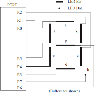
Figure 8.10 Connection of Port Pins to an Array of 8 LEDs Arranged to Show a Hexadecimal Digit in Seven Segment Format
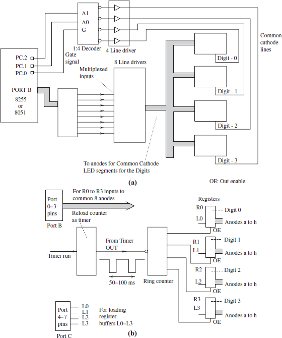
Figure 8.11 (a) Circuit of Multiplexing in a Four-Digit Display and (b) Necessary Steps for Continuous Display by Refreshing Every 50 ms or 10 ms interval
Figure 8.11(b) shows the necessary steps for refreshing the continuous display. A timer ISR is used to generate timing signals to a ring counter. The ring counter outputs OE connect to the common ends of the digits. There is a register for each set of segments in the digits. There are four registers. R0-R3 for buffering the multiplexed output from Port B. The buffer loads the encoding port bits and connects to the LED segments. For example R0 = 1, R1 − R3 = 0 will connect the LEDs of segments b and c only to enable display of 1. L0 − L3 will load the register to select where to display1 For example, L0 = 0, L1 = 0, L2 = 0 L3 = 0, will mean digit 0 be sent to 1.
8.4 ALPHANUMERIC DEVICES—DISPLAY SYSTEMS AND THEIR INTERFACES
Display systems are of three types:
- LED
- LCD
- LCD with touch screen
Display system can be based on 16-segment display system. It is used for alphanumeric displays. Display system can be using dot-matrix displays. It is used for the alphanumeric, graphics, multi-lingual and multifonts display.
8.4.1 Alphanumeric Display by Sixteen-segment Display systems
Seven-segment arrangement (Fig. 8.10) displays only hexadecimal and a few other digits or letters. It cannot display many letters and lower case characters. Further, the current dissipation in seven-segment LED display is high when compared to 16-segment display in LCD.
A 16-segment LCD display can display (i) numeric and letters and (ii) both. It displays the letters, A to Z, 0 to 9, a to z, and the like. Display is by lighting and blanking its segments appropriately. It dissipates very little energy. A liquid crystal is present between two electrodes in two planes (front and back planes). BP means backplane and FP means front plane of an electrode. Each plane has a transparent electrode each. Liquid crystal is encapsulated within it. A sixteen segment alphanumeric character requires 16-control inputs. An alternative is used in place of 16 inputs for the control inputs for each 16-segment BP0 − BP3 and FP0 − FP3 or BP0 − BP3 and FP0 − FP1 signals are used.
Figure 8.12 shows the arrangement of LCD segments to display an alphanumeric character. A row of 16 segments (for example, in a time and date display 08:05:50 Sat. Jul 17, 2004 in a row of 32 alphanumeric characters) or a matrix consisting of rows and columns is needed in many applications (for example, a LCD display in a phone).
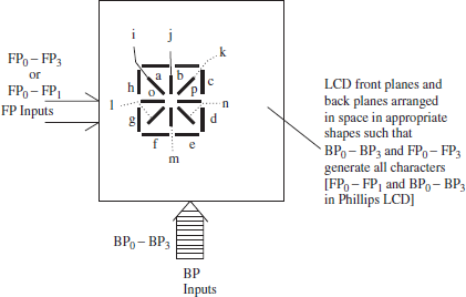
Figure 8.12 Arrangement of LCD Segments When Displaying an Alphanumeric Character in Capital as Well as Lower Case
Program Example 8.6
Let a 16-segment show four characters—M, e, n and u in message at a row of eight sixteen-segment LCDs. What are the segments that will be showing off for each character?
We can glow by programming such that the 8 characters from the left as follows: First character by lighting segments ghikcd for ‘M’, second by segments cbjpme for ‘e’, third by gopd for ‘n’,fourth by defg for ‘u’and fifth to eight characters no segments light up.
8.4.2 Dot-matrix Display Systems for Multilingual, Multi-fonts and Graphic Displays
Sixteen segments (a to p) per digit/character display also has limitations. The characters other than English, symbols, user-defined characters and graphics cannot be displayed. Dot-matrix displays are then used.
Each matrix of dots displays one character. Each dot is one pixel. Each element of the matrix corresponds to one pixel. Let us therefore assume that a character consists of 5 × 7 or 7 × 9 matrix with dots as its elements. A dot either lights up or does not glow (off). Current flowing in a dot lightens a dot up and no current through it switch that off. It enables a general-purpose display text, pictogram as well as graphic displays can be made by dot matrices.
All possible characters are to be displayed by a dot matrix for each character. A ROM stores the 5 × 7 dot matrix corresponding to each character in an array of eight consecutive addressable bytes. The ROM can be called as character ROM when it is used for character graphic bits. The character ROM stores a table for all characters.
Example 8.5
How does the character graphic dot matrix store at the character ROM for character ‘A’?
Figure 8.13(a) shows how a 5 × 7 matrix of 0 or 1 at the dots for ‘A’ and corresponding bytes at the ROM addresses.

Figure 8.13 (a) 5 × 7 Matrix for a and Corresponding Bytes at a ROM Address. (A Dot Element = 1 Means there is Glow at that Position and = 0 Means no Glow from that position); (b) 5 × 7 Matrix for Z and Corresponding Bytes at Another ROM Address and (c) Timing Signals, Counter, Decoder, Address Generator from the ASCII Code and ROM Displaying a Character
How does the character graphic store at character ROM for character Z?
Figure 8.13(b) shows how a 5 × 7 matrix for ‘Z’ and corresponding bytes at another set of ROM addresses.
Display signals: A display signal has 8, 16 or 40 characters with each character given 8 (horizontal) × 8 (vertical) dots space. A set of multiple signals (2 or 4 or more) display a menu or graphics or image like in a mobile phone. A 240 × 64 or 640 × 200 or higher dot matrix LCD displays with built-in controller are used in wide screen LCD display.
Character tables in ROM with dot matrix stored for each ASCII code: There is a character Generator ROM (called font table ROM) with table pointer addresses at input. The characters generate from the ASCII codes in the inputs. A character generates by 8 rows of 8-bits each sent as input to character graphic RAM. For each ASCII code, out of 128 ASCII codes, there is a pointer address for the corresponding character and the ROM provides the output bits for the display matrix at that address. Each display matrix consists of 8 rows with each row having 8-bits as per the character font. Other than English characters and symbols can also be stored in that ROM. Assume English characters at a keyboard. When a key is pressed, its ASCII code is given as upper address bits for the character table ROM. The lower three bits are given by the scan counter outputs. ROM gives the eight-row outputs in the required sequence. Figure 8.13(c) shows how the timing signals, counter, decoder and address generator from the ASCII code and ROM can display a character. Using the counter output byte for each row out of 8-rows for a character is obtained.
Example 8.7
How can the character tables in ROM be used to display?
Figure 8.13(c) shows that for each character there are 8 rows in a character table stored. A timer time-out signal starts a counter, which generates outputs 000, 001, … up to 111. The counter output is the lower address bits for the ROM. The higher address bits are as per the ASCII code of the character. Therefore, for the character to be displayed, 8 bytes are sequentially generated in the output. A character graphic RAM (CGRAM) is then sent these bytes for display.
Character graphic in RAM with display signals in sequence of characters being displayed: The user-defined characters and bytes for a graphic display or for an image are sent to the RAM before the characters are displayed. These bytes at 8-rows/character from ROM are stored at the RAM. RAM stores the bytes, 8 bytes per character, in a sequence required for the display signal or signals. Data for display signal data stores at the RAM addresses in sequence of their display from first dot matrix in first signal to last dot matrix in the last signal. CGRAM also stores pictogram as well as graphic displays.
Refreshing of characters in display signals: A new character might be keyed in after an interval. The CGRAM will be sent bytes for new character also. The character displayed might have to be deleted. Therefore, CGRAM bits are sent for screen-display again and again after short intervals, it is called refresh interval. Refreshing of dot matrix display is also done by a display controller. An LCD controller has all the circuitry, ROM and RAM built into it. Section 8.5 will describe the LCD controller. It enables a general purpose displays. The text, pictogram as well as graphic displays can be made by dot matrices.
Period for display of each pixel: Current pulse for each dot (pixel) is sent for a short interval of time. After that time display of pixel will be off. However, if the current pulse is refreshed again after a short interval then the off-state will not visible in the display to human eyes. This is due to persistence of vision. This is the method by which the total current dissipation in the display system gets limited. Suppose pulse period is 2 ms and it is repeated after 20 ms for a bright pixel, then power dissipated for glow of that pixel is 10%. Pulse period is also used to control the screen brightness.
Coloured display: For a coloured display, in place each dot position will have three elements one red (R), second green (G) and third blue (B).The colour of a pixel corresponds to a combination of R, G and B components.
8.5 LCD AND LCD CONTROLLER
8.5.1 LCD
There are two planes—front and back. Each plane has a transparent electrode each. Liquid crystal is encapsulated within it. A 50 Hz square wave drives a liquid crystal display (LCD) pair of planes.
The AC component is applied using square waves across each plane electrodes. Each plane is applied two wave-forms. One form has both electrode square waves in phase. The LCD display turns OFF in this form as the potential difference between the planes at any instance = 0. Another form has both electrode square waves out of phase 180° out of phase. The LCD display turns ON in this form as the potential difference between the planes varies from a peak value Vp to -V The DC component in square wave is very small with negligible DC current between the front and back planes. The DC component should be < 50 mV.
There are four backplanes and four back plane signals. A pair of signals turns the LCD segment within the pair ON or OFF. The transmission or reflectivity of liquid crystal encapsulated in between the planes changes on a BP and FP signal pair when the pair has out of phase square waves.
There are back plane signals are BP0 × BP3 to display alphanumeric characters in combination with front plane signals. The front plane signals are FP0 × FP1 or FP0 × FP3 in two cases of using 16 segments. (Fig. 8.10). One case is called (1/2) multiplexing and other (1/4) multiplexing for displaying alphanumeric character.
A multiplexing circuit drives the back and front planes. The one-fourth multiplexing needs only 8 interconnections in place of 32 interconnections (16 each from back and front planes in a 16 segment per character display). Motorola LCD display systems follow one-fourth multiplexing. Other example is of a Philips 16 digit and one-signal LCD module. It uses a half instead of one-fourth multiplexing described above. Intersil series LCD drivers use one-third multiplexing. The LCD drivers are built into the controller.
LCD displays are nowadays coloured and wide screen sizes. An LCD display controller is required for the LCD panel or matrix.
8.5.2 LCD Controller Circuit
A typical controller has the circuit characteristics as follows:
- MCU port just sends to controller input the ASCII codes. The codes are sent for the characters in a sequence in which the display of characters occurs.
- A Shift register shifts the display from one to the neighbouring next character till the last character and repeat the displayed character cyclically.
- A Refreshing controller cyclically refreshes the display of each character.
- A Decoder gives signals for a character at an instance. Decoder connects to a ROM . The ROM stores a lookup table. The output bits from an address drive one-fourth of a multiplexing circuit.
- The circuit displays the graphics as well as alphanumeric characters. The RAM at the controller is used to store sequentially display user-defined graphic or special characters. The RAM bytes are written from the character table in ROM.
- The circuit may also connect for the input using the serial port of MCU in place of parallel port.
8.5.3 LCD Controller
Hitach 44780 is a single IC LCD controller. The controller is used in interfacing with the 8051. Optrex DMC 16xx, DMC 16xxx, DMC 20xxx, DMC 24xxx series also have similar pin connections and characteristics. These ICs can also be used to interface 8051 port.
An LCD controller has the following capabilities:
- Accepts ASCII inputs for the characters.
- Controls display of 8 characters (8 × 1) to 80 characters (20 × 4) or (40 × 2). 8 × 1 means 8 characters/line. 20 × 4 means 20 in 4 lines (40 × 2) means 40 in 2 lines.
- Reads and writes the data from and to LCD. Reads the status. Writes the command for the controller.
- Controller can be programmed to accept 4-bit at a time or 8-bit at a time for the ASCII code to be displayed as a character. Eight-bit mode is faster. It needs a minimum of ten pins. The four-bit mode is slower. It needs only a minimum of six port pins. A shift register can be additionally interfaced. It reduces the port pin requirement from 6 to 3.
- E (enable) pulse for period > 0.450 μs. One pulse initiates a data byte or nibble transfer. Two times (one nibble is sent first and then the second) in two pulse per character mode. ASCII code is sent by sending one nibble first and second nibble next.
- Hitachi 44780 has user-defined display for the first 8 characters with code 00H to 07H.
- A register select input RS selects the controller command register if it is 0. It selects internal data register (for data bus buffer) in the controller if it is 1. RS=1 enables reading by the micro controller the currently displayed byte (character) and writing to the current cursor position for the character. [A cursor specifies where the next character is to be written through the data register. It is programmable as invisible or visible and moveable to next on a write or blinking and moveable to next. The cursor if programmed for visibility (or sometimes for blinking) shows the position where the next write can be made.]
- The RS = 0 is used to read by the MCU the execution status and to write the command (instruction).
- Cursor can be programmed to shift right or left after the write operation.
- The instruction set consists of the commands for the clear display, return home, entry mode set, display on/off control, function set, set character graphic RAM (CGRAM) address, set display data RAM address, write data into CGRAM or data display RAM.
- Programmable for 1 signal or 2 signals display.
The LCD controller is programmable for various LCD display control functions. Figure 8.14(a) shows a block diagram of the subunits in LCD controller. The block diagram shows a simple overview (for a preliminary understanding) of the internal hardware. Figure 8.14(b) shows the signals and pin-configuration of the pins at the Hitachi 44780, Optrex DMC 16xx, DMC 16xxx, DMC 20xxx and DMC 24xxx series compatible LCD controller. Table 8.1 gives the different subunits in the LCD controller.

Figure 8.14 (a) The Block Diagram of Subunits at a LCD Controller and (b) Configuration of the Pins and Signals at the Hitachi 44780, Optrex DMC 16xx, DMC 16xxx, DMC 20xxx and DMC 24xxx Series Compatible LCD Controller
Table 8.2 gives the meaning and use of each pin.
8.5.4 Interfacing with LCD Controller
Interface to 8051: Figure 8.15(a) shows the interfacing circuit of LCD controller with 8051. (Only B4 − B7 used in Two times two pulse mode for E pulses. It is when command register is commended for one nibble at one time mode.) The port bits are connected to data buses, RS (D/![]() (data/
(data/![]() ) register select) and E (chip enable) at the controller.
) register select) and E (chip enable) at the controller.
Interface to a processor: Figure 8.15(b) shows the interfacing circuit of the LCD controller with a processor. The address and data buses of a processor are used to interface. RS [(D/C (data/control)] connects to A0 and E (chip-enable) connects to A1-A15 through a decoder. Consider an example. Assume that interface circuit uses the addresses F0C0 and F0C1H at the processor during writing or reading. Decoding is such that when the processor addresses the Hitachi 44780, Optrex DMC 16xx, DMC 16xxx, DMC 20xxx and DMC 24xxx series compatible LCD controller for read or write, then only ![]() = 0, else the
= 0, else the ![]() is 1 when decoder selects other peripheral or memory address. (
is 1 when decoder selects other peripheral or memory address. (![]() means select the chip when it is 0.)
means select the chip when it is 0.)
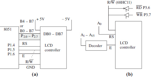
Figure 8.15 (a) Interfacing Circuit of the LCD Controller with 8051 Port Bits Connected to Data Buses, RS [D/C (data/control)] and E (Chip Enable) (b) Interfacing Circuit of the LCD Controller with the Address and Data Buses; RS [D/![]() (data/
(data/![]() )]
)]
Table 8.1 Different Subunits in the LCD Controller
| Subunits | Use |
|---|---|
Data-bus buffer |
An internal buffer register for the data bus. It holds the data byte from the data bus during write and sends the byte to data bus during read operations of the processor. Data byte can be for the control, status or display buffer. |
I/O control when 0) [Read/write control logic] |
I/O control signals are as follows: (a) R/W (to read when 1) (to write the data bus buffer when 0), (b) RS is for sending an ASCII code when RS = 1 and for sending command when 0, (c) E (Enable), it logically activates the controller on a pulse such that it is = 1 for minimum 0.450 μs. E is activated after setting or resetting RS and R/W and after data is ready. |
Control/Status |
Register to send the commands to controller and register to read the status |
RAM (CGRAM) |
User defined characters in the RAM (8 bytes per character) from the top Character generator address. [Top means first address in RAM] |
Controller defined character generator ROM |
Controller defined Character Generator ROM (called Font table ROM). It has input for the pointer addresses for the characters. The characters are generated from the ASCII codes from port inputs through the data bus buffer. |
Timing control logic |
Timing logic for refresh circuitory for display. |
Table 8.2 gives the meaning and use of each pin.
Table 8.2 Pins in Hitachi 44780, Optrex DMC 16xx, DMC 16xxx, DMC 20xxx and DMC 24xxx Series Compatible LCD Controller

Note: aFor sending an ASCII code when RS = 1 and a command when 0. E at beginning set 1 for 0.45 ms or till DB7 bit on reading the status shows 1. IO means input and output pin at port. O means output pin at port.
Table 8.3 gives the addresses as an example. Assume that these selected for interfacing the Hitachi 44780, Optrex DMC 16xx, DMC 16xxx, DMC 20xxx and DMC 24xxx series compatible LCD controller interface.
Table 8.3 Addresses for the LCD Controller
| Direct Address | Explanation of the Function |
|---|---|
0x0F0C0 |
For sending the command words during write at this address and for status bits read from this address by the processor instructions. This address is thus common for command words as well as status byte. |
0x0F0C1 |
For data during write of ASCII code or CGRAM byte at this address into the data register. This code points to a ROM address for bytes for a matrix for character and is for sending to CGRAM address. |
8.5.5 Programming aspects of Hitachi 44780, Optrex DMC 16xx, DMC 16xxx, DMC 20xxx and DMC 24xxx Series Compatible LCD Controller
Programming of controller is must. It is done after powerup reset or power. After power-up, a wait between 10 to 20 ms may be required. After that the command instructions are sent. After each instruction, a delay of ~0.150 ms may be required (~5 ms after clear display instruction or return cursor home instruction).
Once programmed by writing the control words (command instructions), the controller will continue to display as programmed till power down or till reprogrammed by writing a fresh set of control words. LCD controller is first programmed and the control words for the modes and commands are as follows
Writing a command at F0C0H (or to Port) is as per the bits meaning explained in Table 8.4. It will set the mode of display.
Table 8.4 Meaning of Each Bit (or Byte) of Command Instruction 0 (RS (A0) = 0)

a First and second row commands for clear and home takes 4.1 ms (= 5 ms) to execute and other instructions take 0.040 ms (maximum ~0.150 ms in some LCD controller).
b 8-bit mode needs more number of port pins and uses DB7-DB0 pins 14 to 7 at the controller. 4-bit mode needs less number of port pins and uses DB7-DB0 pins 14 to 11 at the controller; high nibble b7-b4 is sent first and then the lower nibble b3-b0 by instructions—SWAP and ANL A, 00FH.
Table 8.5 gives the meaning of status bit read from the port by MCU.
Table 8.5 Meaning of Status Bit (or Byte) Read From the Same Address Where the Commands were Sent (RS (A0) = 0)

Table 8.6 gives meaning of data bits read written at the port.
Table 8.6 Meaning of the Bits when Reading or Writing F0C1H (or to Port) (when RS (A0) = 1)

Notes:
- Wait for 15 ms after power up (wait till status bit b7 (call BF busy flag) shows 0 after E is set to 1).
- Always wait for ~ 0.150 ms (or ~0.050 ms it depends on the controller used) between two instructions for controller read or write. Control word write needs E = 1 for ~ 0.45 μs. Set E = 1 and reset E = 0 in next instruction in normal read write instruction.
- Always wait for ~ 5 ms after clear display or return cursor home instruction.
- Before reading the BF, disable controller by E = 0, write output bit = 1 to DB7 at 8051 port pin, and make E = 1 first and then E = 0 in the next instruction. To reduce the waiting period, poll the BF for 0 before making E = 0.
Examples of the instructions for programming the LCD controller are as follows.
(i) How do you program the LCD controller for 4-bit mode for using the controller pins 14-11 only and fewer port bits? (ii) How will you write ASCII code for display of ‘B’ using four-bit interface mode? (iii) Write clear display command after first programming the 8-bit mode for using the controller and interfacing P2.0-P2.7 to DB0-DB7.
Table 8.4 shows that when R/![]() = 0 and RS = 0, the interface length sets by the DL bit (b4) = 0 when b7-b6-b5 = 001. Assume N = 0 (one display signal), F = 0 (5 × 7 font). Then, the command instruction to be written into the controller is 00100000 (20H). Let controller pin RS connect to Port pin P1.4, R/ W pin to P1.5 and E pin to P1.6. Let P1.0 to P1.3 connect to DB4-DB7 (pins 11 to 14)
= 0 and RS = 0, the interface length sets by the DL bit (b4) = 0 when b7-b6-b5 = 001. Assume N = 0 (one display signal), F = 0 (5 × 7 font). Then, the command instruction to be written into the controller is 00100000 (20H). Let controller pin RS connect to Port pin P1.4, R/ W pin to P1.5 and E pin to P1.6. Let P1.0 to P1.3 connect to DB4-DB7 (pins 11 to 14)
(i) Initialize: |
||
|
CLR C |
;Clear the Carry |
|
MOV P1.4, C |
;RS = 0 Select the register for command instruction |
|
MOV P1.5, C |
;R/ |
|
MOV P1.6, C |
;E = 0 Disable controller interface |
LCDInst: |
MOV A, #20H |
;Accumulator = 20H for the command instruction |
|
MOV R7, A |
;Save accumulator byte at R7 [Stack can also be used.] |
Four-BitInterfaceMode_Set: |
||
WriteUpperNibble: |
||
|
SWAP |
;Swap lower and higher nibbles at A Note A is now 02H |
|
ANL A, #0FH: |
;Make upper nibble at A = 0000b |
|
MOV P1, A |
;Write lower nibble to P1.0 to P1.3, which connects DB4-DB7 |
|
SETB P1.6; |
;Enable controller interface |
|
CLR P1.6; |
; Disable controller interface as one instruction cycle time has lapsed and that is >> 0.40 μs for classic 8051 |
|
ACALL delay |
;Instruction for the DL command may take maximum 0.150 ms, therefore call 0.150 ms delay routine. |
WriteLowerNibble: |
||
|
MOV A, R7 |
;A is taken back from R7 and = 20H |
|
MOV P2, A |
;Write lower nibble to P2.0 to P2.3, which connects DB4-DB7 |
|
SETB P1.6 |
;Enable controller interface |
|
CLR P1.6 |
;Disable controller interface as one instruction cycle time has lapsed and which is >> 0.40 μs |
Delay 0.150 ms: |
;Instruction for the DL command may take maximum 0.150 ms |
|
(ii) ASCII code for ‘B’ is 42H. We set RS = 1 for moving the ASCII code for the display |
||
|
SETB C |
;Set the Carry |
|
MOV P1.4, C |
;RS = 1 Select the register for data |
|
CLR C |
;Clear carry |
|
MOV P1.5, C |
;R/ W = 0 Write mode for data |
|
SETB P1.6; |
;Enable controller interface |
|
MOV P1.6, C |
;E = 0 Disable controller interface |
LCDData |
MOV A, # 42H |
;Accumulator = ASCII code for ‘B’ |
|
MOV R0, A |
;Save accumulator byte at R0 [Stack can also be used.] WriteUpperNibble: |
Same instructions as in the previous program for upper nibble |
||
Call delay 0.150 ms routine |
||
WriteLowerNibble: |
||
Same instructions as in the previous program for lower nibble |
||
Delay 0.150 ms: |
;Call routine for delay = 0.150 ms |
|
(iii) (a) The command instruction to be written into the controller is 00110000b (30H) for eight bit interface mode. Let controller pin RS connect to Port pin P1.4, R/ |
||
|
CLR C |
; Clear the Carry |
|
MOV P1.4, C |
;RS = 0 Select the register for command instruction |
|
MOV P1.5, C |
;R/ W = 0 Write mode for command instruction |
|
SETB P1.6; |
;Enable controller interface |
|
MOV P1.6, C |
;E = 0 Disable controller interface |
LCDInst1: |
MOV A, #30H |
;Accumulator = 30H for the command so that 8-bit interface length sets |
Eight-BitInterfaceMode_Set: |
||
|
MOV P2, A |
;Write LCD instruction to the port |
|
SETB P1.6; |
; Enable controller interface |
|
CLR P1.6; |
;Disable controller interface as one instruction cycle time has lapsed and that is >> 0.40 ms |
Delay 0.150 ms: |
;Call routine for delay = 0.150 ms |
|
LCDInst2: |
M0V A, #00H |
;Accumulator = 00H for the command so that display clears |
|
MOV P2, A |
;Write LCD instruction to the port |
|
SETB P1.6 |
;Enable controller interface |
|
CLR P1.6 |
;Disable controller interface as one instruction cycle time has lapsed and that is >> 0.40 ms |
;Call routine for 5 ms delay. |
||
Program Example 8.8
How will you use the busy flag BF at status-register in LCD controller so that the extra delay introduced to wait for guaranteed completion of the write instruction can be minimized?
Table 8.5 shows that when R/![]() = 1 and RS = 0, b7 shows busy flag BF when the controller is busy. We can poll the busy flag in place of introducing the delay. Polling is by an instruction—JB P2.7, −2 in the following program. Let controller pin RS connect to Port pin P1.4, R/ W pin to P1.5 and E pin to P1.6. Let P2.0 to P2.7 connect to in DB0-DB7 (pins 7 to 14).
= 1 and RS = 0, b7 shows busy flag BF when the controller is busy. We can poll the busy flag in place of introducing the delay. Polling is by an instruction—JB P2.7, −2 in the following program. Let controller pin RS connect to Port pin P1.4, R/ W pin to P1.5 and E pin to P1.6. Let P2.0 to P2.7 connect to in DB0-DB7 (pins 7 to 14).
The algorithm will be as follows:
Step 1: If power-up took place within 15 ms, wait.
Step 2; Initialize R/ ![]() = 1; RS = 0 and E = 0.
= 1; RS = 0 and E = 0.
Step 3: Set Port pin P2.7 as output = 1 (It is required in 8051 before using the same pin for the input).
This instruction does not affect the controller as E is reset to 0 currently at step 2.
Step 4: Wait loop till P2.7 input = 0.
Step 5: Initialise R/ ![]() = 0 again for write to the controller and exit the polling program.
= 0 again for write to the controller and exit the polling program.
Step 6: Write the data or instruction byte.
8.6 TOUCH SCREEN AND TOUCH -SCREEN CONTROLLER
LCD display screen is nowadays coloured, wide screen size. There are touch plates on the display. The plates are over the LCD screen in the touch screen based displays. The touch screen is widely used in mobile, Pocket PCs, computers and control panels. Pocket PC uses the LCD for dot-matrix display for showing keys and menu. There are touch screen plates on the display screen. Touch screens also have the applications in heavy industry, sales terminals and ATM bank machines. These are used where the keyboard and mouse pose difficulty. A touch screen provides fast and accurate interaction between the users with the contents displayed.
8.6.1 Touch Screen
A touch screen is an input device. It is used as a convenient alternative to or keypad or keyboard. A touch screen is used in combination with display system in mobile, Pocket PCs, computers and control panels. The touch screen is an input device, which is combined with a display and a PC or other device to make a complete touch-based input-output system. When using the touch screen, a stylus is used for inputs. Stylus is a pencil-shaped object, which is touched at the screen, which displays the keys or menu items, buttons, sliders and wheels on the screen. The finger can be used to touch and select. This is when screen-displayed characters or buttons are big in the size (nearly equal to finger thickness). There are two types of touch screens—single touch and multi-touch.
The touch screen has four units:
- Touch-sensor unit
- Touch screen controller
- Touch screen driver software
- Software functions library to enable developing the applications
Touch Sensor Unit
A sensing unit at touch-screen consists of a transparent glass surface. The surface is sensitive to touch. The touch sensor unit is just over the display screen and panel is of same size as of display panel. There are five common methods used for sensing the touch—(1) Capacitive, (2) Mutual capacitive, (3) Self capacitance, (4) 4-wire resistive and (5) 5-wire resistive.
(1) Capacitive method: Figure 8.16 shows a capacitive touch-sensing unit. On the display panel, there is glass base of same size as display panel.
(i) Over the base there is a conducting layer (layer 1). (ii) Over the pattern there is a layer of dots (layer 2). Dots are small, transparent and insulating. (iii) Over this layer, there is another conducting layer (layer 3). (iv) On this layer, there is conducting material coating layer on the poly film (layer 4). (v) Over it there is a hard coat surface film. Capacitive touch sensing between layer 4 and 1 uses the signals acquired by charge-transfers between Z+ and Z−. A touch panel is coated with a transparent but conducting material thin layer (layer 3). There is another layer below that (layer 1) and an electrostatic field is applied between the layers. There are electric lines of forces between the layers. Capacitor charges are at two layers 1 and 3. As human body conducts, when a finger is brought at a point on the panel, the charge will fiow through that. The electrostatic lines of forces in space between 1 and 3 are changed. This change in capacity causes the charge transfers between Z+ and Z− and touched finger. The change in current is detected by the signal acquired by the controller. The capacitive sensor disadvantage is that they get affected by intense light. It needs touch by a conductive body or stylus. They can be used with LCD as well as CRT (Cathode ray tube).

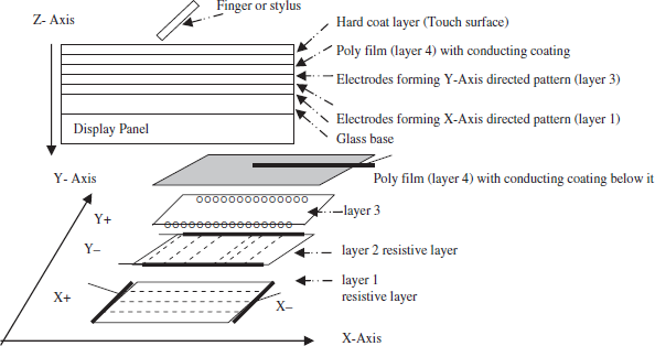
(2) Mutual capacitance method: Figure 8.17 shows a mutual capacitances touch sensing unit. Mutual capacitance touch-sensing unit contains a grid of parallel sensing lines and parallel driving lines. The mutual capacitances found between the two sets of lines are used to detect the touched (x, y) position on the screen. On the display panel, there is glass base of same size as display panel. (i) Over the base there are conducting rectangular strips (layer 1). The strips form the electrodes directed along the X-axis. All electrodes directed along the X-axis are connected to sensing lines. (ii) Over the pattern there is layer of dots (layer 2). Dots are small, transparent and insulating. (iii) Over this layer, there are rectangular strips of electrodes (layer 3) directed along directed along the Y-axis. All electrodes directed along the Y-axis connect the driving lines. (iv) This set of Y-directed electrodes is the coating over a poly film (layer 4). (v) Over poly film there is hard coat film. A mutual capacitance touch-screen panel is thus composed of 2 layers of X-directed and Y-directed layers with sensing and driving lines. X and Y strips are separated by a narrow gap (due to dots). When a stylus or finger, touches the hard- coated surface, it compresses the poly film and space between the dots and one of the X-pattern plate electrode at layer 1 comes in contact with Y-pattern plate electrode at layer 3. The charge transfer takes place between conducting human body and layers 1 and layer 3 functions as a pair of charge transfer dividers. The change in mutual capacitances is used to detect single or multiple touches (simultaneously) on the screen as the touch events. A touch screen supports up to 64 sense channels (Screen area can be divide into 64 positions and that can be touched on the screen. Detector will find which of the 64 positions has been touched along the X and Y-axes. Response time is about 4 ms (less than 15 ms). There is very low power dissipation during idle state (< 1.8 mW). The mutual capacitance method is also known as projected Capacitive Touch (PCT) technology.

(3) Self capacitance method: Figure 8.18 shows a self capacitance based touch sensing unit. Self capacitance uses one layer of individual electrodes connected with capacitance-sensing circuitry. The self capacitances between the grid pattern electrodes is used to detect the touched (x, y) position on the screen. On the display panel, there is glass base of same size as display panel. (i) Over the base there is (layer 1) with series of rectangular electrodes directed along the X and Y-axes. All electrodes connect to sensing lines and driving lines. (ii) This layer is coated over the poly film (layer 4) called bonding layer. (iii) Over poly film there is hard coat film called protective layer. The method is also known as projected capacitive touch (PCT) technology. When a stylus or finger, touches the hard-coated surface, it compresses the poly film and space between the dots and one of the plate electrode at layer 1 comes in contact with human body or conducting stylus. Thus, layer 1 electrodes show changes in self capacitances between driving and sensing electrodes (rectangular strips). The changes are used to detect as the touch events.
The changes in the currents due to charge transfers to touched positions are detected by a controller for processing. The change causes the voltage changes, which is detected by ADC channel in the controller.
(4) Resistive four-wire method: Figure 8.19 shows four-wire resistive touch sensing unit. On display panel, there is glass base of same size as display panel. (1) Over the base there is conducting resistive layer (layer 1) with electrodes forming a voltage gradient directed along the X-axis. (2) Over the layer, there is layer of dots (layer 2). Dots are small, transparent and insulating. (3) Over this layer, there is resistive layer (layer 3) with electrodes forming a voltage gradient directed along the Y-axis. (4) This layer is coating over the poly film (layer 4). (5) Over the poly film there is a hard coat film. A resistive touch-screen panel is thus composed of 2 layers resistive layers 1 and 3, separated by a narrow gap (due the dots). When a stylus or finger, touches the hard-coated surface, it compresses the poly film and space between the dots and one of the X-pattern plate electrode at layer 1 comes in contact with Y-pattern plate electrode at layer 3. Thus layers 1 and layer 3 function as a pair of voltage dividers, which are connected to the output. This causes a change in the electrical current. The change is used to detect as a touch event (interrupt to controller).
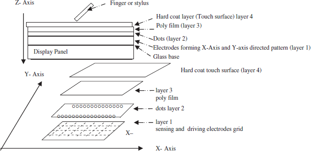

Figure 18.19 Four Wire Resistive Touch Sensor
There are four wires Y+, Y−, X+ and X−. Y+ is connected (pulled up) to Vcc through much high resistance compared to sheet resistances. Step 1: Vcc is applied high voltage and X− is ground, when there is no touch, Y+ voltage is high. Step 2: When there is touch; Y+ pin gets connected to the ground through a low resistance path. Hence, Y+ voltage is low. This generates an interrupt to the touch-screen controller. Step 3: Y+ is applied driving voltage and Y− is ground. There is voltage gradient along the Y-axis. Voltage is read at X+ and is proportional to Y-coordinate of touched position. Step 4: High voltage is applied to X+ and X− connects to ground. Voltage is read at Y+. It is proportional to x-coordinate of the touch position.
The change is sent to a controller for processing. The change causes the voltage change, which is detected by an ADC in the controller. The resistive touch sensor advantage is that they are not affected by intense light. They don’t need to be touched by a conductive body or stylus only. Insulating touch pencil can also be used. They have longer life compared to other sensors. Response time is less than 10 ms. Four-wire method is used with CRT (Cathode ray tube).
(5) Resistive five-wire method: Figure 8.20 shows a five-wire resistive sensing unit. On the display panel, there is glass base of same size as display panel. On the display panel, there is glass base of same size as display panel. (1) Over the base there is conducting resistive layer (layer 1) with electrodes forming a pattern directed along the X-axis. (2) Over this layer, there is resistive layer (layer 2) with electrodes forming a pattern directed along the Y-axis. (2) Over the pattern there is layer of dots (layer 3). Dots are small, transparent and insulating. (4) Over this layer, there is a poly film coating layer (layer 4). It is coated with conducting layer. (5) Over it there is hard coat film. When the screen is touched, it pushes the conductive coating on the coversheet against the coating on the glass, making electrical contact. The voltages produced are the analog representation of the position touched. Five-wire resistive technology involves a glass substrate overlaid with a suspended polyester cover sheet. It is simple. It is easy to measure the touch coordinates.
There are five wires Z, Y+, Y−, X+ and X−. Z is connected to ADC. Step 1: Y+ is applied high voltage and X− is ground, when there is no touch, Z voltage is low. Step 2: When there is touch; Z pin gets connected to resistance paths to Y+, Y−, X+ and X−. Hence, Z voltage is high. This generates an interrupt to controller. Step 3: Y+ is applied high voltage and Y− is ground. There is voltage gradient along the Y-axis. Now Z is measured. Z is proportional to the y -coordinate. Step 4: X+ is applied high voltage and X− is ground and voltage is read at Z and it is proportional to the x-coordinate of the touch position.
This change in resistance causes the voltage change, which is detected by the ADC in the controller. The resistive sensor advantage is that they are not affected by intense light. They don’t need to be touched by a conductive body or stylus only. Insulating touch pencil can also be used. Response time is less than 15 ms. The resistive sensor advantage is that they are not affected by intense light. They don’t need to be touched by a conductive body or stylus only. Insulating touch pencil can also be used. The five-wire touch screens can be used with LCD as well as CRT (Cathode ray tube).
Capacitive sensing is robust. Mutual and self capacitive touch-screens also support multi-touch. Resistive touch-screens typically have a high resolution (4096 × 4096 DPI or higher). Other methods for the touch systems are as follows:
(1) Infrared can also be used in optical-touch systems. Arrays of LEDs emit infrared (IR) and phototransistors detect the IR rays. These are placed on two adjacent edges of a display. This detects the event of touch. The array forms a grid of IR beams across the display. An object (finger or stylus) on touching the screen intercepts the IR rays. The measured outputs can be used to locate a touch-point coordinate. (2) Strain gauge method can also be used. (3) Optical imaging method is that two or more image sensors are placed at the edges. Optical images are taken by tiny cameras. Infrared rays are emitted and touch shows the shadows at the optical images. (4) Mechanical vibrations on glass can be detected, and the vibrations are used to detect a touch event; any object can be used to generate these events, including fingers and stylus. The method used to detect is a dispersive signal method. (5)Acoustic pulse recognition method is based upon generation of mechanical vibrations using three or more piezoelectric crystals and detecting the propagation periods between detected and transducers.
8.6.2 Touch-screen Controller
A single-touch device is controlled by Atmel AT42QT4120 and AT42AT4160. It support screen sizes of up to 4.3″ with aspect ratios of 16:9 or 4:3. Aspect ratio means ratio of height to width of the screen. Figure 8.21 shows a touch-screen controller.
A controller is an IC-based card. MCU is single-cycle RISC AVR core with 32 registers and engine that process the x and y positions on the touch-screen. It interfaces between the touch sensing unit and the computer of mobile or other microcontroller system. It receives analog inputs from the touch sensing and converts it in the output to a serial/COM port (PC) or to a USB port (PC or Macintosh). The controller is according to interface required for a system. Resistive or capacitive touch-screen controller has two components—acquisition and control. Acquisition part contains X-sense/drive and Y-sense/ drive lines a DSP control and processor. Control part contains oscillator, RAM, CPU, fiash memory, power management circuit, and I2C and GPIO (general-purpose IO) interfaces. ADC is two/four channel with Vref+ and Vref− outputs (Fig. 8.21).

8.6.3 Touch-screen Software Driver
A touch-screen driver is a software update for the system. The system connects to the touch-controller through serial or GPIO interfaces. The driver enables the touch screen to function along with the existing system. It facilitates new applications to be developed. The driver enables the touch-screen and system to function together.
Inputs from touch screen: The driver enables the operating system to interpret the touch event and touch x, y positions. It enables touch screen to emulate the mouse click as a touch. This makes touching the screen the same as clicking a mouse at the same location on screen. The touch on the screen is analogous to mouse cursor movement plus click at the x, y point on the screen. The double touch or stylus tap is analogous to double-click with mouse. The drag using finger or stylus from a point to another is analogous to drag-and-drops with mouse. The touch-screen driver can be programmed for analogous to left or right mouse clicks.
8.6.4 Software Functions Library to Enable Developing of the Applications
Atmel released QTouch library version 3.0 in 2009. It is for touch-interface application. It is a free software. QTouch library can be downloaded from Atmel’s touch software product page at www.atmel.com/qtouchlib. It has following features (www.atmel.com):
- Designed for capacitive touch sensing using charge-transfer signal acquisition with robust sensing
- Support for up to 64 sense channels.
- Includes debouncing software for touch keys.
- Includes adjacent key suppression method for the unambiguous detection of key events.
- Support for a range of Atmel MCUs, tinyAVR®, megaAVR®, XMEGA™, UC3A, UC3B.
- Supports both QTouch and QMatrix™ for touch and handwriting acquisition methods.
- Gives fiexible choice of touch sensing functionality (keys, buttons, menus, sliders, wheels) in a variety of combinations. The QTouch library stores pre-compiled object code binaries. These can be configured individually as touch keys or combined in groups to form sliders or navigation functionality.
- 256-level slider or wheels using only 3 channels.
- The QTouch Library enables customization and optimization of the touch function by the user. The precompiled software libraries come with a defined application programming interface (API).
- Common API across all library versions.
8.6.5 Multi-touch and Multi-touch Controller
Two touch devices AT42QT5320 and AT42QT5480 are manufactured by Atmel. They support screen sizes of up to 8″ with a 16:9 aspect ratio. Atmel two-touch controller ICs can track and report one or two simultaneous touches as separate X and Y positions. Common user-initiated gestures including tap, double tap, fiick and drag, as well as two-touch gestures such as zoom in, zoom out and rotate are implemented in the touch-screen controllers.
Atmel makes ICs which are known as maXTouch controllers. mXT224 is capacitive touch-screen controller. It has two components—acquisition and control. Acquisition part contains X-sense and Y-drive lines, a DSP control and processor. Control part contains oscillator RAM, CPU, fiash memory, power management circuit’ I2C and GPIO interfaces. CPU is single-cycle RISC AVR core with 32 registers. DSP has two on-chip DSP engines that process the x and y positions on the touch screen (Fig. 8.22). Controller has following features:
- Excellent signal-to-noise ratio 80:1 SNR and high response (4 ms and 250-Hz video-screen refresh rate).
- 224 nodes that allow it to accurately report the positions of unlimited simultaneous touches, and it can completely redraw the screen every 4 ms.
- Very small 10 μW sleep mode, less than 2 mW in idle and less than 4 mW fully active touch modes power dissipations.
- Give real-time characteristics. Their applications are in handwriting recognition, video games and other applications which require high response and performance of the controller.
- Functionalities for stretch/pinch and rotate gestures, handwriting, shape recognition, face detection and rejection of unintended touches.
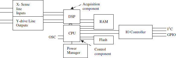
Figure 8.22 MaXTouch Controller
8.6.6 Virtual Keypad
One of the applications of touch screen is to display a virtual keypad.
Example 8.8
Picture 8.1 shows a pocket PC that shows a new way of keying in the data through a displayed keypad on the screen. It is HPIPAQh5400 Pocket PC for VOIP using Pocket PC. VOIP is for voice over IP applications.
New generation mobile has touch screen. It has very few keys only and uses virtual keypad. Virtual keypad is a keypad appearing on the touch screen and touching by finger is at the key of virtual keypad. It results in actions similar to actual keypad.
Example 8.9
One of the application of touch screen is to select a menu. An LCD dot matrix touch screen displays the graphic user interface. Siemens SX56 Pocket PC in Picture 8.2 shows wide screen display with a menu.
Picture 8.1 HPIPAQh5400 VIG0 V0IP Pocket PC for Voice over IP Applications.


8.7 KEYBOARD-CUM-DISPLAY CONTROLLER (8279)
We learnt the following in Section 8.1. The states of the keys are found by sending the scan signals to keys and receiving the sensed signals [Section 8.1]. A keyboard has many keys. There is need for two pairs of encode and decoder for scan and sense signals in case of a keyboard. There is the need of remove effects of bounce (debouncing) from each key.
There is need of continuous scan of the rows and columns in keyboard. When the keys are pressed in quick succession, there is need to save the state of each key. ASCII code for the pressed state of each key is put in a queue. Queue is a data structure, which is used as first-in first out (FIFO).
There is need for N-key rollover. A hardware interface chip is required to store after correct parse (search) the key or sequences of the keys pressed by a user.
We learnt the following in Section 8.3. The glowing of various segments in a two-dimensional 7-segment display has to be according to a specific pattern as per the numeric character or hex-digit. There is the need for multiplexing and refreshing in case of a multiple-digit display.
Keyboard with the display of the pressed key(s) or the results of the commands keyed-in by sequential key pressing are required for human-computer interaction. Software approach was shown in the Program Examples 8.1 to 8.5. This approach needs the processor time to execute the instructions. It needs additional memory space.
8.7.1 Keyboard-cum-display controller 8279
The 8279 IC is a popular keyboard-cum-display controller IC. It has two control units—one for keyboard and the other for display. The 8279 has the following capabilities:
- Interface up to sixty-four push-button or contact keys.
- There are eight return (sensing) signals (columns).
- There are four scan signals.
- Four scan signals if connected to a decoder in a mode called scan signal encoded mode gener ates 16 signals (16 addresses of the rows).
- There is one control/strobe key and one shift signal making it effectively 8 scan signals (rows).
- Debouncing of each key is done by hardware.
- There is FIFO buffer to store a byte each in queue on successive key contacts on pressing.
- Interrupt generates on each FIFO entry (each key-read operation).
- Two-key lockout or N-key rollover mode. Two-key lockout is the default set mode on chip reset.
- Sensing at the return signal in place of the key contact can also be from a sensor like phototransistor (to detect light presence), Hall effect (to detect magnetic filed), ferrite core (to detect displacement). Return signals and scan can be programmed for sensor mode or keyboard mode. In a keyboard mode, the debouncing effects are taken into account.
- Right-side entry means when the number of digits increases, the character for the first in-contact key displays at the right side place and shifts to left on successive key contacts. Left-side entry means when the number of digits increases, the character for the first in-contact key displays at the left side place and shifts to right on successive key contacts. Left-side entry is the default set mode on chip reset. Display can be programmed for left-side entry as in a text display or right side entry as in a calculator.
- There is 16 × 8 (16 byte) internal RAM. This facilitates 16-character scanned display, which interfaces the LEDs.
- Programmable 8-character multiplexed display or 16-character multiplexed display.
The 8279 is a programmable chip for various keyboard and display control functions. Figure 8.23(a) shows the block diagram of subunits at 8279 chip. The block diagram shows a simple overview (for a preliminary understanding) of internal hardware. Tables 8.7 to 8.9 give the meanings and use of subunits shown in the block diagram.
Table 8.7 The Meaning and Use of the Set of Subunits for Interfacing the Bus and for IO, Timing and Control Shown in the Block Diagram
| Subunits | Use |
|---|---|
Data-Bus Buffer (top row-left side) |
An internal buffer register for the data bus. It holds the data byte from the data bus during write and sends the byte to the data bus during read operations of the processor. |
I/O Control (middle rows left side) and Read/write control logic |
I/O control signals are as follows: (a) |
|
It connects to A0 address signal of processor address-bus (after latching AD0 using ALE). When it is 1, the data bus buffer writes into the control (command) or reads the status register. When it is 0, the data bus writes (when |
|
(i) RESET (to reset the programming logic of 8279), it connects to processor resetout. It also default sets the two-key lockout mode and left-side entry mode. (ii) CLK (clock) for the 8279, it connects to a CLK control signal of the processor (For example, XTAL2 in 8051 as shown in Fig. 2.17). |
Control and timing Registers (top row subunit at right side) |
To control and set the timings the registers store the display and keyboard modes and conditions of operation. Basic counter chain exists for the timings. |
Timing and Control (bottom row subunit at right side) |
Sends the timing signals to RETURN unit, keyboard debounce and control unit and scan counter. Sends as output a signal BD for blanking displays. |
Table 8.8 The Meaning and Use of the Keyboard Section Subunits Shown in the Block Diagram
| Subunits | Use |
|---|---|
FIFO/SENSOR RAM Status (bottom row subunit at left side) |
8x8 FIFO/SENSOR RAM connects through the internal data bus and to keyboard debounce and control signal. IRQ (Interrupt Request) output from it to processor on a FIFO entry. IRQ sets to 1 when the FIFO has at least one entry pending the read operation by the processor. IRQ becomes 0 after a read from RAM and becomes ‘1’ again if an entry is pending for the read. |
FIFO/SENSOR RAM(middle row subunit at left side) |
RAM to store 8-bits sensed in a FIFO of 8 bytes for eight entries at keyboard entries. The processor reads the bytes from the FIFO RAM. |
Keyboard and STB Debounce control (middle row subunit at middle) |
Gets inputs from the return signals RL0-RL7 and SHIFT and CNTRL/ signals through the RETURN subunit. Gets two signals—from timing control subunit and from Control and Timing Registers subunit. It debounces and outputs to FIFO/SENSOR RAM. |
RETURN subunit (bottom left side) |
When a key is pressed and contact is made, the eight return and two status signals SHIFT and CNTRL//STB are sent to this subunit. Signals are as follows: (a) RL0-RL7 eight return signals after the scan of the keyboard, (b) SHIFT signal with status = 0 or 1 information, internally pulled high and key closure may pull it down to 0 (c) CNTRL//STB signal with status = 0 or 1. In strobe input mode, the data enters in the FIFO. |
SCAN COUNTER subunit (at bottom external circuit left) keyboard |
Gives outputs SL3-SL0 four scan signals. It can be programmed in two modes. Encoded mode in which these signals, which decodes by an decoder (near the keyboard or display) into the 16-signals to display. It increments from 0000, 0001, 0010, … 1111 in one scan cycle. It drives the 16 rows of keys as well as drives 16 digits in case of multiplexed display. Decoded mode in which these signals are already decoded by an internal decode and scanning is from 0001, 0010, 0100, 1000 in one scan cycle and is for four rows only. |
Table 8.9 The Meaning and Use of the Display Section Subunits
| Subunits | Use |
|---|---|
DISPLAY address register (middle row subunit at middle) |
Stores from the internal data bus the display address for sending into 16 × 8 RAM [16 characters of 8 bits each.] |
DISPLAY 16 × 8 RAM (middle row subunit at display right side) |
16 × 8 RAM [16 characters of 8 bits each], which sends the Out A0-Out A3 and Out B0-Out B3 signals to display unit through the registers. The processor writes into the RAM the bytes for the display of the characters and reads the bytes at the RAM. |
DISPLAY registers (bottom row subunit at left side) |
Sends the Out A0-Out A3 and Out B0-Out B3 signals to display unit. |
Figure 8.23(b) shows the pin-configuration of the pins at the 8279 chip. Table 8.10 gives the meaning and use of each pin
Table 8.10 Pins in 8279

b From FIF0 RAM.
c Control (Command or status)/Data Buffer address signal.
d Programmable as 16- character multiplexed or 8-character multiplexed
e Programmable as single 8 bit b7-b0 (B3-B0 as b3-b0 and A3-A0 as b7-b4) as in a 7-segment digit or dual 4-bit (A3-A0 and B3-B0).
Table 8.11 gives the addresses for the 8279 interface when F0A0 and F0A1H are the addresses used by processor for writing or reading. Decoding is such that when the processor addresses the 8279 chip for read or write, then only ![]() = 0, else it is 1 when processor bus signlas are meant for other peripherals or memory addresses.
= 0, else it is 1 when processor bus signlas are meant for other peripherals or memory addresses.
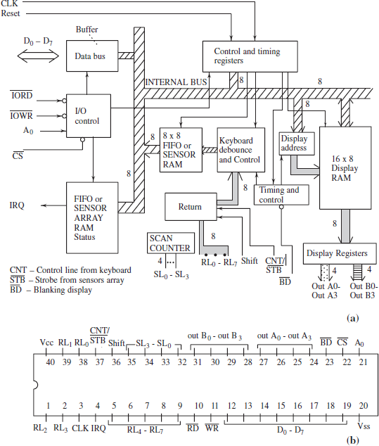
Figure 8.23 (a) The Block Diagram of Subunits at the 8279-chip and (b) Signals and Configuration of the Pins at the 8279-chip
Table 8.11 Function of the Addresses for 8279 Keyboard/Display Controller interfaced to a processor
| Direct Address | Explanation of the Function |
|---|---|
0x0F0A0 |
For data during write at this address into the display RAM and for data reception during read from this address from the FIFO/SENS0R RAM by the processor instructions. This address is thus common for display buffer as well as keyboard buffer in 8279. |
For sending the command words during write at this address and for read of status bits from this address by processor instructions. This address is thus common for command words as well as status byte in 8279. |
8.7.2 Interfacing of 8279
Figure 8.24 shows the interfacing circuit of the 8279 chip with the address and data buses A0 [C/![]() (control/data)] connecting to A0 and CS (chip-select) connecting to A1-A15 through a decoder and with the keyboard and displayed digit matrices.
(control/data)] connecting to A0 and CS (chip-select) connecting to A1-A15 through a decoder and with the keyboard and displayed digit matrices.
Figure 8.25(a) shows a part of the interfacing circuit of the 8279 chip with a keypad of 4 rows and 4 columns. Figure 8.25(b) shows another part of interfacing circuit of the 8279 chip with a display of four digits hexadecimal.
8.7.3 Programming Aspects of 8279
Programming is must for 8279 after power-up reset. Once programmed by writing the control words (for the mode and command instructions, it will continue to work as programmed till power down or till reprogrammed by writing a fresh set of control words.

Figure 8.24 Interfacing Circuit of the 8279 chip with the Address and Data Buses and with the Keyboard and Displayed Digit Matrices
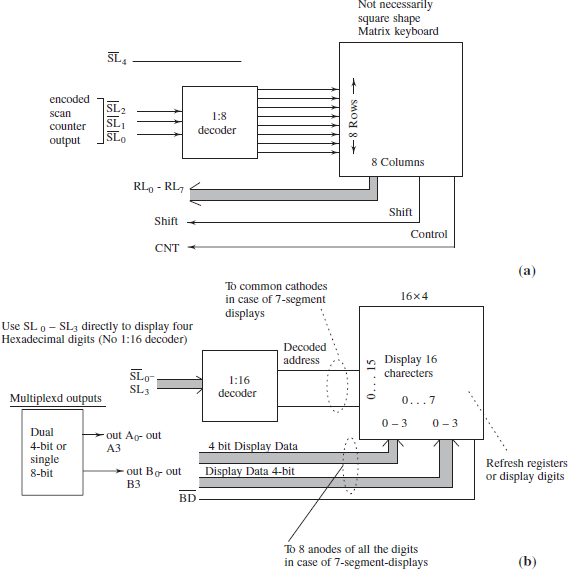
Figure 8.25 (a) A part of the Interfacing Circuit of the 8279 Chip with a Keypad Consisting of the 4 Rows and 4 Columns. (b) Another Part of Interfacing Circuit of the 8279 Chip for a Display of Hexadecimal Four Digits
- 8279 is sent initialisation instructions byte before read of a keyboard entry. The initialisation is done using the write instruction of processor for data buffer. The entry is read using the read instruction of processor for data buffer.
- 8279 reads status bits (byte) for the status by the read instruction of processor.
8279 is first sent initialisation instructions for (i) keyboard mode, (ii) display mode, (iii) program its clock timings for a divisor value, (iv) starting address of RAM and how should it increment, (v) read instruction and (vi) inhibiting and blanking format.
Programming is as follows for control words for modes and commands:
- Suppose, the address of control word is F081H. Then, during the move of a byte to F081H, A0 will be 1, and A1-A15 decodes accordingly to select the 8279.
- Suppose, the address of RAM for the FIFO/SENSOR RAM as well as Display RAM is F080H, then during the move of a byte to F080H, A0 will be 1, and A1-A15 decodes accordingly to select the 8279.
Writing keyboard/display mode command is done. [The command bits meaning explained in Table 8.12]
Table 8.12 Meaning of Each Bit of Mode Instruction as Keyboard/Display Mode when b7, b6 and b5 = 0
| Bit Position | Name | Explanation of the Function |
|---|---|---|
b7, b6, b5 |
— |
= all 0s means keyboard/display mode set as per b4 and b3 (DD) for display and b2, b1 and b0 (KKK) for keyboard |
b4, b3 |
DD |
= 00 means eight number 8-bit character displays with left side entry |
b2, b1, b0 |
KKK |
= 000 means encoded scan keyboard with 2-key lockout |
Table 8.13 gives the meaning of bits in the instruction for setting of program-clock.
Table 8.13 Meaning of Each Bit of Instruction for Program Clock Setting when b7 and b6 = 0 and b5 = 1
| Bit Position | Name | Explanation of the Function |
|---|---|---|
b7, b6, b5 |
— |
= 001 means program the clock |
b4, b3, b2, b1, b0 |
PPPPP |
= 5 bits if all 1s, then divisor is 31. 10000 means 16. 1f clock input is 1 MHz, then 01010 means clock divisor = 10, then 100 KHz is the internal timing clock in 8279. For example, it then sets out the keyboard time = 5.1 ms (after 5 ms, the scan counter changes) and debouncing time of 10.3 ms. |
Table 8.14 gives the meaning of bits in the instruction for reading of FIFO/Sensor RAM.
Table 8.14 Meaning of Each Bit of Instruction for Reading FIFO/Sensor RAM after a Scan on Setting when b7 = 0 and b6 = 1, b5 = 0 and b3 = 0 or 1
| Bit Position | Name | Explanation of the Function |
|---|---|---|
b7, b6, b5, b3 |
— |
= 0, 1, 0 and 0 or 1, respectively, means read FIFO/Sensors RAM after a scan |
AI |
AI is auto increment flag. It can be 0 or 1 (it does not matter) in keyboard mode. The 8279 automatically increments and drives the data bus for each subsequent read in same sequence as the keys are pressed. [Data buffer Read is by address signal A0 = 0 and |
|
b2, b1 and b0 |
AAA |
Any of the A can be 0 or 1 (it does not matter) in the keyboard mode. A has to be defined. 000 means read from SENSOR RAM address 000 in sensor mode. 010 means address 010. |
Table 8.15 gives the meaning of bits in instruction for reading of the display RAM.
Table 8.15 Meaning of Each Bit of Instruction for Reading Display RAM Setting b7 = 0 and b6 = 1, b5 = 1
| Bit Position | Name | Explanation of the Function |
|---|---|---|
b7, b6, b5 |
— |
= 0, 1 and 1, respectively, means read display RAM |
b4 |
AI |
AI is auto increment flag. AI = 1 will auto increment the address at AAAA of internal display RAM automatically on the successive reads. AI = 0 will not auto increment the address at AAA of internal display RAM automatically and for the successive reads from the RAM, the AAAA must be defined. |
b3, b2, b1 and b0 |
AAAA |
A has to be defined. 0000 means read from Display RAM address 0000. 0100 means read from display RAM address 0100. |
Table 8.16 gives the meaning of bits in the instruction for writing the display RAM.
Table 8.16 Meaning of Each Bit of Instruction for Writing the Display RAM on Setting when b7 = 0 and b6 = 0, b5 = 0
| Bit Position | Name | Explanation of the Function |
|---|---|---|
b7,b6,b5 |
— |
= 1, 0 and 0, respectively, means write display RAM by writing into the data bus buffer by instruction for which A0 = 0, CS = 0 and WR = 0. |
b4 |
AI |
AI is auto increment flag. AI = 1 will auto increment the address at AAAA of internal display RAM automatically on the successive writings. AI = 0 will not auto increment the address at AAA and for successive writings into the display RAM, the AAAA must be defined. |
b3,b2,b1 and 0. |
AAAA |
A has to be defined and 0000 means read from Display RAM address. 0100 means read from display RAM address 0100. |
Table 8.17 gives the meaning of bits in the instruction for inhibit/blanking display write.
Table 8.17 Meaning of Each Bit of Instruction to Display Write Inhibit/blanking on Setting when b7 = 1 and b6 = 0, b5 = 1
| Bit Position | Name | Explanation of the Function |
|---|---|---|
b7, b6, b5, b4 |
— |
= 1, 0, 1 and (0 or 1), respectively, means display write inhibit/blanking as per the following rows: |
IW-IW |
IW = 1 for one of the ports (OUT A3-A0) or (Out B3-B0) not effected by the display RAM entry. Therefore, IW-IW = 0 1 means for (Out B3-B0) not effected by the display RAM entry. IW-IW = 1 0 means for (Out A3-A0) not effected by the display RAM entry. IW-IW = 1 1 means for (Out A3-A0) and (Out B3-B0) nibbles both not effected by the display RAM entry. IW-IW = 0 0 means for (Out A3-A0) and (Out B3-B0) nibbles both effected by the display RAM entry. [Default IW-IW on reset = 0 0.] A3 corresponds to b7 at RAM entry, A0 to b4, B3 corresponds to b3 at RAM entry and B0 to b0. |
|
b1, b0 |
BL-BL |
BL = 1 for one of the ports using (Out A3-A0) or (Out B3-B0) blanked for display. BL, BL = 1 1 means both the ports using (Out A3-A0) or (Out B3-B0) blanked for display. 0 and 0 means none blanked. 0 and 1 mean blank Out B3-B0 nibble only. 1 and 0 mean blank Out A3-A0 nibble only. |
|
[Default BL-BL on Reset = 0 0.] |
The reader can refer the data sheet for 8279 for full details.
An initialization instruction example is as follows:
Program Example 8.9
(i) How do we program the 8279 for 16 keys arranged as 4×4 in the N-key rollover mode? (ii) Set the internal divisor to 10. (iii) How will you read a key from the FIFO RAM? (iv) Read a key. Assume addresses used for 8279 are 0xF080H and 0xF081H. Display is for 8-bit 8 characters left entry.
8279 does not need any external scan signals decoder for 4×4. Therefore, according to Table 8.12 first part KKK bits (b2, b1 and b0) = 011. (b7, b6 and b5) = 000. Taking DD = 00, the command bits should be 000 00 011. The 8051 assembly program will be as follows:
- Keyboard_DisplayMode_Set:
M0V DPTR, #0F081H
;Load memory address pointer as F081H
M0V A, # 03H
;Program the keyboard mode in A register
M0VX @DPTR, A
;Write command for keyboard mode
- Refer Table 8.13 for program-clock instruction. The PPPPP bits (b4, b3 b2, b1 and b0) = 01010 for divisor = 10. Command bits (b7, b6 and b5) = 001. The 8051 assembly program will be as follows:
Clock_Divisor_Set:
M0V A, # 2AH
;Program the clock divisor = 10 decimal in A register
M0VX @DPTR, A
;Write command for keyboard and display mode
- Refer Table 8.14 for Read FIFO instruction. Assume that AI and AAA bits do not matter. The command bits (b7, b6 and b5) = 010. The 8051 assembly program will be as follows:
Read FIFO_Set:
M0V A, # 40H
;Program the FIFO. All bits are irrelevant except b7, b6 and b5.
M0VX @DPTR, A
;Write command for keyboard and display mode
- Refer Table 8.14 for Read FIFO entry through address F080H from the data bus buffer. The 8051 assembly program will be as follows:
Read_FIFO Entry:
MOV DPTR, #0F080H
;Load FIFO RAM pointer as F080H
MOVX A, @DPTR
;Read data for keyboard FIFO entry.
8.8 INTERFACE WITH PRINTER
A printer has following units—internal print controller, RAM circular buffer, font-table ROM and one of the standard interfaces.
Print controller: Print controller is a single-purpose processing unit. It has control ROM. The control ROM stores the instructions for controller. It controls the communication among the printer controller, RAM, ROM and serial interface (or Centronics) signals.
RAM: RAM is used by print controller. RAM stores the circular buffer. RAM also stores the stack and temporary variables.
Circular buffer: The circular buffer means as follows: It is a memory buffer at RAM. The bytes are sent from buffer address 0 to N−1 identical to the ones sent into a queue. At the start the head and tail pointers are at address 0. The bytes are printed from tail of a queue and inserted at the head of queue at buffer. The following are the operations:
- Each time a byte is inserted from queue, the head pointer increases. Each time a byte is printed (called deletion from queue), the tail pointer increases. On insertion of the Nth byte the pointer for head is at address N−1. On printing of the Nth byte the pointer for tail is at address N−1.
- When a byte after the N bytes is inserted then the head pointer moves from N−1 to 0. When a byte after the N bytes is printed then the tail pointer moves from N−1 to 0.
- The insertion and printing of bytes again starts from step 1 and from address 0 after the head pointer address reaches N−1.
- The printing of bytes again starts from step 1 and from address 0 after the tail pointer address reaches N−1.
Font-table ROM: There is a ROM to keep the font table with 8 bytes for each character in ASCII code table, as the case with display controller ROM.
ROM is a character font generator ROM (called font table ROM) with table pointer address at input. The characters generate from the ASCII codes in the address inputs at ROM. A character generates by 8 rows of 8-bits each sent as the input to a character graphic RAM. For each ASCII code, out of 128 ASCII codes, there is a pointer address for the corresponding character and the ROM provides the output bits for the dot matrix at that address. Each dot matrix consists of 8 rows with each row having 8-bits as per the character font. Other than English characters, symbols can also be stored in that ROM.
A printer may be using one of the standard interfaces—Centronics parallel or RS232C Serial or USB or wireless USB.
8.8.1 Parallel Centronics Interface — A Printer Interface
Figure 8.26 shows the Centronics interface to a printer. Centronics interface is parallel interface for printing. It has 36 lines and Centronics connectors have 36 pins. 15-pins are used as follows: There are 12 logic ground pins, one connector chassis ground one Vcc and one analog ground pin. Other 15-pins are used as follows: All 8 data are sent in parallel. Interface has data bus D0-D7 8 lines. Seven lines are Reset, Select, Ready, Acknowledge, Busy, Page error and Error. The resetting signal when it is 0 resets the controller.
D0 to D7 are the bit (data) during the parallel transfer of the commands and instructions to the RAM. Before D0-D7 bits are accepted, the two handshaking signals (strobe and acknowledgment) are used. The status signals from print controller are Busy and PE (paper enable and paper error).
A computer or MCU can send the commands and characters in ASCII codes through Centronics interface to a printer controller. The printer can print at the speed compatible to its mechanical assembly. When the buffer gets full, the computer stops the communication on an interrupt or busy signal from the printer. As and when more and more empty spaces are created in the buffer, the not-busy signal is sent to the computer and the computer starts sending bytes to those spaces.
8.8.2 Serial RS232C Interface for a Print Controller in a Printer
Figure 8.27 shows RS232C interface to a printer.
RS232C deploys a 9 or 25 pin connector in an IBM PC. A computer or MCU can send the commands and characters in ASCII code to print controller. These are processed in the controller similar to a display controller.

Figure 8.26 Centronics Parallel Port Interface for Printer

Printer controller for RS232C serial interface can provide for the programmable baud rates. Interfacing is through UART serial communication mode. Baud rate can be 110, 300, 600, 1200, 2400, 4800 and 9600 baud per second.
The following seven signals are interfaced through a 9-pin connector:
- Serial interface voltage levels for 0s can be 15V> V> 3Vthrough TxD (transmit data) and RxD (receive data) pins. Serial interface voltage levels for 1s can be for −15V < V < −3V through TxD (transmit data) and RxD (receive data) pins.
- Five handshaking pair of signals are as follows: (i) (CTS, RTS), (ii) (DTR, DSR) and DCD. DCD pin signal is a carrier detect signal. The handshaking signals are identical to ones 8251 signals (Section 7.1). Handshaking signals for 1s and 0s are at TTL levels—2.4V < V < 5V and 0V < V < 0.8V, respectively.
8.9 PROGRAMMABLE INTERFACE FOR INSTRUMENTS USING IEEE488 (GPIB) BUS
IEEE 488 is a standard bus, originally developed by Hewlett Packard and is called the general-purpose interface bus (GPIB). Figure 8.28(a) shows the GPIB bus for the GPIB interfaced instruments. The GPIB deploys 24 signals, which interface to the GPIB controller and MCU.
The controller controls the programmable instruments, which are interfaced using GPIB. These can function, using the controller as a talker or listener or both. Figure 8.28(b) shows the sequences of signals on GPIB bus. GPIB bus can interface the number of instruments that have GPIB IEEE488 interface in them.
Table 8.18 gives the bus signals (24 signals) for data, handshaking and management.
A controller uses ATN handshake signal. DB0-DB7 are the bus signals. When ATN = 1, 7-bit address is placed on the bus. When ATN = 0, 8-bit data is on the bus. The handshaking signal-sequences for communication are as follows:

Figure 8.28 (a) GPIB-interfaced Instruments Using 24 Signals, which Interface to the GPIB Controller and MCU and (b) Signal- Sequences on the GPIB Bus
- Let t1 be the instance when device (talker) asserts DAV (makes = 1) to indicate data-available. Assume that at t1, some other device (listener) has already asserted NRFD (by pulling and making = 0). This is due to listener not yet ready for the available data. Therefore, the NDAC = 0 and it is because the valid data has not yet been accepted by listener. Data bus now carries an address up to the instance t0.
- Let t2 be the instance when NRFD pulled up = 1. This is because the listener is now ready for the data made available by the talker. At t0 instance, the data bus now carries data.
- As soon as this happens, at immediate next instance t3, the DAV pulls down = 0. The valid data is now there to the listener.
- At the next instance t4, the listener pulls down NRFD = 0 when it is reading the valid data.
- At the next instance t5, listener accepts data and pulls NDAC = 1 (= 0 earlier because 0 indicated that data not yet accepted).
- At next instance t6, the receiver can again assert the next byte of data using DAV and thus making the next byte available on the bus.
- At instance t1, the address is again carried on data bus and the above cycle can repeate.
Table 8.18 (a) IEEE 488 GPIB Signals for Data
| Signals | Function | Direction and Use |
|---|---|---|
DB0-DB7 Data Bus 8 signals |
Data |
For sending address, commands or data to and from the addressed instruments (Maximum data transfer rate of 1 MB/s). [The commands enable (i) a device to become source of data (talker) and, (ii) any combination of the remaining devices to become the acceptor of data (listener).] |
8 GND Signals |
Ground |
For return path for the signals |
(b) Handshaking and Management Signals
| Signals | Function | Direction and Use |
|---|---|---|
DAV |
Data available |
From GPIB controller or talker to listeners, whenever a valid data is on the data signals |
NRFD |
Not (yet) Ready For the Data |
A logic ‘0’ from a device; ‘1’ when ready (to listener) |
NDAC |
Not (yet) Accepted the Data |
A logic ‘0’ from a device (listener) that is busy in reading data from the data signals; ‘1’ when reading is over |
IFC |
Interface Clear |
From the controller, stop (the current bus activity) request bus management signals |
SRQ |
Service Request |
From a device to a controller to get service. [It is like interrupt to enable use of the bus] |
ATN |
Attention |
From a new device or controller that intends to talk through the bus |
REN |
Remote enable |
To select remote or local control of a device |
EOI |
End or Identify |
To indicate end of an operation or to identify by polling a device by a talker or listener. |
8.10 INTERFACING OF 8051 MCU WITH EXTERNAL MEMORY
Sections 3.4.(3) and 3.4.(4) had given the details of interfacing the external memory. Figure 8.29 shows interfacing circuit of 8051 with ROM and RAM external memory. Interfacing is done by the following signals:
- The
 (External Enable) pin is set to 1 when (i) internal ROM is also to be used and (ii) external memory chip is extending the internal ROM by providing new addresses. The (External Enable) pin is set to 0 when (i) internal ROM is not being used for program store and (ii) external memory chip all addresses from 0x0000 are used for program store. The (External Enable) pin (Fig. 2.2) in 8051 versions with fiash memory is the /Vpp pin. The is reset to 0 if only external addresses are to be used.
  is connected to
  (read) Read pin of ROM.
- AD0-AD7 bus signals are the inputs to a latch (74LS374). Latched output is used to connect A0-A7 pins of the ROM.
- ALE is connected to latch enable signal at latch.
- Higher address A(8 + m) to A15 bits from P2 are connected to a decoder and the decoder output connects the ROM.
- Lower address bits from A8 to A8 + m −1 are connected to ROM where m depends on capacity. A ROM of 4 kB needs 12 address lines, A0-A11. If capacity is 4 kB, thus m is 4. If ROM capacity is 16 kB, then m is 6. If capacity is 32 kB, then m is 7.
- Higher address A(8 + m) to A15 bits from P2 are connected to a decoder and the decoder output connects the RAM.
- Lower address bits from A8 to A(8 + m −1) are connected to RAM where m depends on RAM capacity. A RAM of 4 kB needs 12 address lines, A0-A11. If the RAM capacity is 4 kB, m is 4. If RAM capacity is 16 kB, then m is 6. If RAM capacity is 32 kB, then m is 7.
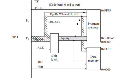
Figure 8.29 External Data and Program Memory Interfacing with the 8051
- Port P0 pins connect D0-D7 inputs of the ROM.
- Port P0 pins connect D0-D7 inputs/outputs at 8-pins of RAM.
 (P3.6) is connected to Out-Enable (read) Read pin of RAM. and are connected to AND gate when RAM is used for control store (Program memory as well as data memory). Otherwise, is connected to pin of ROM and to pin of RAM.
 pin (P3.7) is connected to pin at the RAM. pin is connected to RAM. also connects the program memory if fiash or EEPROM needs to be written.
8.11 INTERFACING WITH FLASH MEMORY
Flash and EEPROM are non-volatile memory. They don’t loose the data on power failure. They write the data byte only if it has been erased previously. Erase means writing all 8 bits = 1s at the addresses of bytes being erased. Erasing is must in both before writing or programming a new byte at an address. Flash memory has ability to erase full sector at an instance. EEPROM requires the byte-by-byte erase. Some EEPROM can, however, be programmed for erase of one, sixteen or more bytes at an instance.
Section 3.4(3) gives the details of interfacing the external program memory. Figure 8.30 shows the interfacing circuit of 8051 with a fiash. Port pins connect D0-D7 inputs of the fiash in the interface. The Vpp pin connects Vpp of the fiash and to a +5 V or +12 V supply. The address and data bits are sent to the flash using the port pins and switching the Vpp on for the needed period during the write. The written data is verified before the next cycle for another address (usually by incrementing the previous address) and data write. The connections for interfacing are done as follows:
- The (External Enable) pin is set to 1 when internal ROM or fiash is also to be used and external memory chip is extending the internal ROM of fiash by providing additional addresses. The (External Enable) pin (Fig. 2.2) in 8051 fiash versions is the /Vpp pin. The is reset to 0 if only external addresses and no internal are to be used.

Figure 8.30 Interfacing Circuit of 8051 with a Flash (n = 8 + m)
- and connected to Out-Enable (read) Read pin of ROM through an AND gate.
- Port P0 pins AD0-AD7 bus signals are the inputs to a latch (74LS374) and the latched output is used to A0-A7 pins of the fiash. ALE is connected to latch enable signal at latch.
- Higher address A(8 + m) to A15 bits from P2 are connected to a decoder and the decoder output connects the fiash. m = n − 8 (Fig. 8.30). Lower address bits from A8 to A(8 + m − 1) are connected to fiash where m depends on capacity. A fiash of 4 kB needs 12 address lines, A0-A11. If capacity is 4 kB, m is 4. If fiash capacity is 16 kB, then m is 6. If capacity is 32 kB, then m is 7.
- Port P0 pins connect D0-D7 inputs of the fiash.
- Port pins P3 connect to , prog. Pulse and program pins of fiash memory. pin (P3.7) is connected to pin at the RAM. pin is connected to RAM. also connects the fiash or EEPROM to be written. Flash programs by setting-resetting bit at P3.2 to P3.5.
Interfacing with fiash memory (or EEPROM) is required in many applications needing a non-volatile saving of the generated or captured data or in-program altered codes or constants by the MCU.
- The data captured in a process may have to be stored in the fiash. For example, in an ECG machine the captured ECG waveform is saved in the fiash. The photo captured in digital still camera is saved in fiash.
- In a process, there are multiple stages, the status of the previous stages successfully completed may have to be stored in the fiash or EEPROM. The data of completed stage is stored in the EEPROM so that in case of power failure further action starts from the left-over stage. (For example, in a washing machine there are three stages—wash, rinse once or twice and dry.)
- The user-defined program for a process may have to be stored in advance in the fiash. For example, in a washing machine the program for the (a) wash stage and other stage periods as per the cloth type, (b) rinse once (in water-saving mode) or twice and (c) drying stage spin or non-spin mode and slow centrifuge or fast centrifuge action speeds, is stored in the fiash.
8.11.1 Programming the Flash Memory Chip
ATMEL AT89C0x51 is an MCU with fiash memory. Reset pin RST is kept between +5 V and +12 V during programming. P3.3 and P3.4, P3.5, P3.6 and P3.7 are used for the control signals for programming the fiash. P3.2 (PROG pin) is the program pin where a program-pulse is sent. Programming means data at D0- D7 saves at a fiash memory address. Erasing means data at all bits become = 1 at fiash memory addresses.
Erase the sectors in flash: The fiash is erased by a control command as follows: Make P3.3 = 1 and P3.4, P3.5 and P3.7 = 0s. Then a program pulse at P3.2 (PROG pin) = 0 for minimum 10 ms interval. RST/Vpp = 12 V
Programming a byte: When a code is written in the fiash, the control command is as follows: P3.3 = 0 and P3.4, P3.5 and P3.7 = 1s and then a program pulse at P3.2 (PROG pin) = 0 pulse (1 to 0 then 0 to 1) in presence of RST. Vpp = 12 V
Writing lock bit 1: When the write lock bit 1 is written, then program memory cannot be written in the fiash, unless it is erased again. Lock bit1 protects the programmed memory from accidental change. P3.3, P3.4, P3.5 and P3.7 = 1, P3.2 PROG pin is sent 0 pulse (1 to 0 then 0 to 1) in presence of RST. Vpp = 12 V for writing lock bit 1.
Read only: When pins P3.1 and P3.2 = 1s and P3.3 and P3.4 = 0s and P3.5 and P3.7 = 1s then the chip can be read (verified), what is programmed, when P3.7 (![]() ) becomes 0 during execution of the memory read instruction. RST = 5 V.
) becomes 0 during execution of the memory read instruction. RST = 5 V.
Writing lock bit 2: When the write lock bit 2 is written then the fiash memory for program codes can not be verified and invalid data is returned, until the chip is erased. Lock-bit 2 is to protect the chip from copying. Make prog. pins P3.3 and P3.4 = 1s, P3.5 and P3.7 = 0s and then P3.2 PROG pulse pin is sent 0 pulse (1 to 0 then 0 to 1) in presence of RST Vpp = 12 V for writing lock bit 2.
8.12 INTERFACING WITH MCU IO PORT USING OPTOISOLATOR
There is a need to protect and isolate the MCU from the following:
- Transient surges
- Larger signal inputs (for example, ~ 30 V)
- Mistakes like an input shorted to the power signal (220 V or 110 V)
- Large input offsets, for example, 440 V
MCU Port IO Pin and interfaced physical system are isolated using an optoisolator. The optoisolator- based circuit and Input-Output Module based on the optoisolator provides the required protection and isolation as well communication between IO pin and physical sysetm.
Optoisolator: When a port output connects to an interfacing circuit, it is important that it is isolated from the induced signals from the interfaced physical system. For example, if a port pin is connected to an interface circuit of a motor, the motor at the start-up or shut-down generates induced-transient signals. An optoisolator transistor provides the optical isolation.
Figure 8.31 shows an optoisolator circuit. The optoisolator has a built-in infrared LED (IR LED) at the input terminals, and there is a built-in phototransistor (FPT) at the output terminals. The FPT faces the LED. The medium in between the LED-FPT pair is fully transparent and the pair surroundings are sealed from any external radiation.
The optoisolator works as follows. The MCU port output = 0 switches ON the LED. The FPT will instantly start conducting, giving logic 0 voltage level at the collector because of conduction of current between C and E. Then, let MCU port output = 1 to switch OFF the LED. The FPT will instantly stop conducting, giving logic 1 at the collector and no current through it. The electrical insulation between the input terminals P and N and output terminals C and E is very high (4 kV and above).
8.13 INTERFACING WITH INDUCTIVE CIRCUIT
The microcontroller port pin needs to interface to a coil in several applications. The following are the examples: (i) coil is used in an ON-OFF relay. (ii) A magnetic field generating solenoid coil is used in an LVDT (linear variable differential transformer). LVDT is used for measurement of displacement, (iii) A coil is used in a magnetically operated valve, (iv) A loud-speaker has a coil, which moves a magnet with frequencies in audioble range. and (v) A set of coils are used in a stepper motor. When current in the coil is switched ON or switched OFF, there is sudden change in current. A sudden change in current across an inductor causes a high voltage transient. The high voltage can damage electronic components. The reason for generation of high voltage transient is as follows:

Suppose there is a coil inductance = L, i is current induced and di/dt is rate of change in i as a function of time t. Then the induced voltage in it is proportional to −L × di/dt. Initially the di/dt is very high when the current switches OFF or ON. Therefore, the special isolation is needed between MCU and coil circuits.
Figure 8.32 shows two interfaces for inductive circuit. The port-pin output of MCU can be 1 or 0 and connects an optoisolator as shown in Figs. 8.32(a) and (b). The output transistor of each interface drives a power transistor. The coil is placed between the collector of power transistor and supply voltage VCC. A reverse biased diode is placed across the coil. This is a must for providing a current-shorting path when the induced voltage transients occur. Without that an excessively high voltage may occur. The transients occur when the MCU instructions set or reset the bit is at instance of 1 to 0 and 0 to 1 logic transitions. A Darlington transistor pair handles the 2 W output in the interface circuit. The power output drives by the +12 V and −12 V supplies.
8.14 INTERFACE FOR A LOUDSPEAKER
Figure 8.33 shows an interface circuit for an output port bit to drive a low-power loudspeaker. Figure 8.34 shows an interface circuit for an output port bit to drive high-power loudspeaker. A speaker has a coil. Assume that it can deliver maximum 2 W sound output. When a port bit is toggled by an appropriate tune-playing software, the speaker generates the musical tones. A reverse biased diode across the coil prevents transient voltages across the collectors C1 and C2 of the transistors.

Figure 8.32 (a) Interfaces circuit to an inductive coil of a solenoid (b) Interface circuit to inductive coil in a relay

Figure 8.33 Interface circuit to a low power speaker driving coil

Figure 8.34 Interface Circuit for an Output Port Bit to a Power Loudspeaker
8.15 INTERFACING THE KEYPAD AND SPEAKER IN A MUSIC PLAYING SYSTEM
A music play system interface is shown in Fig. 8.35. The circuit of Fig. 8.35 consists of two interfaces. One is for the keypad and another for speaker. Software for the keypad can be designed to work in two modes.
Mode 1 is the musician (or practitioner or child player) mode. The musician presses a key for a note for generating that particular note for a period. For each note, the frequency of toggling 1s and 0s at the port output pin differs. Generation of music is by playing different notes using the fingers. The keys are pressed in definite sequences with definite intervals needed as per the musical tune. Using a command key, the sequences of the keys and intervals of the keys can store a musical tune generated by the musician.

Figure 8.35 (a) Interface to a Coil to Low Power Speaker and (b) interface to a keypad and loud speaker in a music notes play system.
Mode 2 is stoned music play back mode. The player just presses a single key to start playing the stored musical tune for a period, say, for 120 s. On pressing the key again, the box will reproduce the same tune again for another 120 5. Pressing another key will play another stored tune. Eight keys can play eight different tunes. The interface hardware is simple but embedded software is the heart of the music player cum box.
Mode 3 can be used to define the note durations and generate the tunes for the different types of the musical instruments using the same interface.
8.16 INTERFACE FOR STEPPER MOTOR(S) IN A ROBOT OR PRINTER OR INDUSTRIAL DRIVE
A robot can have three or four stepper motors. A printer has two stepper motors—one to drive the roller of the printer (and thus the paper) and second one to drive the print head stepwise after printing a character. Let us consider a four-pole stepper motor. There is a coil corresponding to each pole. The coils A, B, C, and D are given the currents through an interface circuit. Figure 8.36 shows the interface circuit for four coils in a stepper motor. Figure 8.37 shows the interface circuit for four stepper motors in a robot.
A stepper motor rotates one step (or half step) at an instance. A motor step angle can be 1.8°. For full rotation of 360°, it will take 200 steps. A stepper motor is easier to control by the simple programs.
Assume that a four-pole stepper motor has coils A, B, C and D and are given the current cyclically as given in Table 8.19 at the successive instances T0, T1, T2. Table 8.19 shows the action at the next instances when the current switches in the different coil. 1 means current ON and 0 means OFF. Program Examples 8.10 and 8.11 are the programming examples for rotating the stepper motor in one step at an instance in a given mode. A port bit is set or reset by the program. Consider a Port Pn and pins Pn.x (n is the port number and x is the port bit number. x can be 0, 1, 2 and 3 for A, B, C and D). A quad of port pins connects the four coils as shown in Fig. 8.37. EN0, EN2, E3 and EN4 send the enabling bits to a set in a motor.
Table 8.19 Stepper Coils A, B, C and D Given the Current Cyclically at the Successive Instances T0, T1, T2, … Rotating in One direction

Stepper coils A, B, C and D Given the Current Cyclically at the Successive Instances T0, T1, T2, … Rotating in Another Direction

Program Example 8.10
Move a stepper motor 1 successively. The motor moves by one step at each instance using 8051 instructions.
SETB P1.4 instruction enables motor 1 steps. The 8051 first two instructions are MOV A, #11H, MOV Pn, A; and after an appropriate delay routine call, an instruction RLA will rotate the motor one step on change from T0 to T1. Assume that motor moves clockwise. Running these instructions in a loop will move the motor in successive steps.
|
SETB P1.4 |
|
ROTATE_CLOCKWISE: |
|
|
|
MOV A, # 11H |
;Move 0001 000 in Accumulator |
|
MOV P1, A |
;Port bits as per A. The coil currents as per lower nibble |
Figure 8.36 Four Interface circuits from port pins P1.0. P1.1, P1.2, P1.3 and P.7 to four coils of stepper motor
|
CALL DLY |
;Call delay routine as motor needs some time to move one |
|
|
;sequence to another |
|
RLA |
;Move motor 1 |
|
AJMP ROTATE_CLOCKWISE |
|
DLY: |
||
Program Example 8.11
Move a stepper motor 2 successively by one step at each instance. Use 8051 instructions to move in the opposite direction with respect to previous example.
SETB P1.5 instruction enables motor 2. The 8051 instructions MOV A, #11H, MOV Pn, A; and after an appropriate delay routine an instruction RR A will rotate the motor one step on change from T0¢ to T1¢. Assume that motor moves anti-clockwise. Running these instructions in a loop will move the motor in successive steps.
|
SETB P1.5 |
|
ROTATE_ANTICLOCKWISE: |
|
|
|
MOV A, # 88H |
;Move 1000 1000 in Accumulator |
|
MOV P1, A |
;Port bits as per A. The coil currents as per lower nibble |
|
ACALL DLY |
;Call delay routine as motor needs some time to move one |
|
|
|
|
RRA |
;Move motor 2 |
|
AJMP ROTATE_ANTICLOCKWISE |
|
DLY: |
||
8.17 ANALOG INPUTS INTERFACE WITH THE MCU
Analog inputs can be from the thermocouple, load cell, ECG sensor and blood pressure sensors. Analog inputs can be from multiple sources. We have learnt that a multi-channel ADC is an ADC, which can receive the analog inputs obtained from number of sensors and transducers. We may use the external ADC chip to interface the MCU. (Section 7.4) MCU units in certain versions have multi-channel ADC unit on-chip (Section 2.3.10).
Figure 8.38 shows the ADC interface for generating digital bits after conversion. The ADC can receive analog inputs from the multiple sources, even though one of it is shown in the figure. The converted bits from analog input so that converted bits are proportional to analog input or analog-input changes. The ADC is also given Vref+ and Vref− inputs.
- Vref+ = maximum value of analog input which generates after conversion all bits = 1s. Vref− = minimum value of analog input and which generates after conversion all bits = 0s.
- The ADC input is from sample and hold amplifier. The sample input is from the output of an OPAMP (signal conditioner). OPAMP input is from a transducer, for example, thermocouple or motor speed sensor or furnace temperature sensor or ECG sensor or load cell sensor.
8.17.1 Interfacing Thermocouple
Thermocouples are widely used in the industry for measuring high temperatures. A thermocouple j unction at source temperature connects to the arm of a Wheatstone bridge. A thermocouple second junction at surrounding temperature connects to another arm of the Wheatstone bridges. A thermocouple generates analog input for the ADC. The input is as per the temperature difference between two junctions J1 and J2 of a thermocouple. Measurement of temperature at J1 can be done if J2 temperature is fixed. J2 is kept at the surrounding room temperature, which is nearly fixed, showing little variations. The variations can be compensated as follows:
When surrounding temperature changes, the J2 temperature changes. The measured temperature at J1 can be different from actual. In order to take this effect on potential difference into account, a temperature compensator is used for compensating the surrounding reference J2 temperature variation. A thermistor is a resistance based temperature detector (RTD). Thermistor is used as resistance between the thermocouple wires at J2 end and is in one of the arm of Wheatstone bridge. It is used as one of the resistance in a Wheatstone bridge. When J2 temperature varies, the existing potential difference also changes as R of the RTD change due to variation in the difference in temperatures at J1 and J2. This compensates the variation in surrounding temperature at J2. Figure 8.39 gives an interfacing circuit for a thermocouple with a surrounding temperature change compensator.
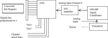
Figure 8.38 ADC method of converting bits from analog input so that converted bits are proportional to analog input or analog-input changes
8.17.2 Interfacing Load Cell— Electronic Weighing Machine
Figure 8.40 gives an interfacing circuit for a load cell. The load cell is in the arm of a Wheatstone bridge. An electronic weighing machine uses a load cell and the resistance of the cell is measured by first generating the analog signal in a Wheatstone bridge. A weighing machine consists of a load cell, display unit and a keypad with four or five keys. The load cell is positioned just below the pan. The pan carries the load. In a child weighing machine (Fig. 1.6), the pan bears the load of the child.
8.17.3 Interfacing - Precision Weighing Machine
Figure 8.41 shows the weighing machine interface circuit elements. These are load cell interface, keypad interface, display interface, ADC interface and serial RS232C interface. The RS232C interface is used to connect the circuit to a computer during calibration. A chemical weighing machine in a pharmaceutical industry requires high precision. The load cell characteristics may vary a little due to spring loosening, for example, due to mechanical corrosion. The periodic recalibration may therefore be required in precision balances. A computer program calculates the offset, proportionality coefficient and non-singularity coefficients. Then, it reprograms the parameters in the EEPROM/flash memory within the MCU using the RS232C interface of the MCU.
8.18 ANALOG OUTPUT GENERATING INTERFACE WITH MCU
Section 7.6 described externally interfaced DAC (digital to analog converter) in Section 7.6. Section 2.3.9 described on-chip PWM in the MCU. On-chip PWM along with an external integrator generates analog output. Analog output can thus be generated either by external DAC chips or PWM in MCU.
Figure 8.42 shows the external DAC method of generating analog output. The DAC is also given Vref+ and Vref− inputs.

Figure 8.39 Interface to thermocouple amplifier

Figure 8.40 Interface to load cell


Figure 8.42 External DAC method of generating analog output
- Vref+ = maximum value of analog output which is obtained when all bits = 1s. Vref− = minimum value of analog output and which is when all port bits = 0s.
- The DAC output is connected to OPAMP input and OPAMP gives the analog output for an external actuator (for example motor or furnace).
Figure 8.43 shows the PWM method of generating analog output. When using an MCU, the analog output is mostly generated by first generating a PWM output and then integrating that. Assume that there are the pulses of pulse-height 5 V. Assume that the pulses have duty cycle 25%. This means that pulses have logic 1 (5 V) for 25% of the period of wave and 0 (0 V) for 75%. When the pulses of duty cycle 25% are given to an integrator with gain =1, the analog output from integrator will be 25% of 5 V That means we get 1.25 V for 25% duty cycle of pulses. When the pulses of duty cycle 50% are given to an integrator with gain =1, the analog output from integrator will be 50% of 5 V An analog output is therefore proportional to pulse width for the period p%.

Figure 8.43 PWM method to generate analog output from the pulses whose width is modulated such that width for period p% is logic 1
Figure 8.43 shows method to generate analog output from the pulses whose width is modulated such that for width for period p% the logic state is 1. An 8-bit pulse accumulator can be used to accumulate pulses at a regular interval, say 8 μs. There are two events at the pulse accumulator. Assume C0 = p × 256/100. Assume first is count C = count loaded in a register C0. Second event is when the pulse accumulator overflows and recounts from 0. PWM unit functions as follows: When pulse accumulator count C reaches a value p × c0 on first event, PWM pin output becomes L =0 and when the accumulator overflows at 256 counts on second event, L =1. Again the cycle starts. Till the pulses accumulate up to c = c0 the output L = 1 but when counts becomes equal again, the PWM output becomes = 0. The PWM output duty cycle is p%. PWM output pulses on integration will give an appropriate analog output.
Generating positive and negative analog output voltages: The integrating amplifier can also be designed such that the analog output is proportional to (p −50)% when the counts c0 = p × 256/100 is loaded in the register. This enables both + and − outputs.
8.19 USING PWM FOR DC MOTOR CONTROL
Figure 8.44 shows an interface circuit. A DC motor can move in both directions—clockwise and anticlockwise. The interface circuit in the figure controls the speed as well as direction of the motor.
Refer Sections 8.18 and 2.3.9. MCU pin output is generated as PWM (pulse width modulated) output. These can be used to obtain positive and negative dc output after integration circuit. Figure 8.44 shows that PWM output L first interfaces first to a dual NOT gate (for buffering). It then interfaces a NAND gate at input-1 pin. Another input bit at the NAND1 is for controlling the motor ON/OFF. It connects output from the microcontroller port pin, say, P1.7. It is input-2 to the NAND1. If ON/OFF input is 0 the output is always 1 irrespective of the PWM signal (first input). If control input is 1, the NAND1 gate output = 0 and 1 as per 1 and 0, respectively at the PWM output.
The NAND1 output interfaces to one terminal A of the motor. The output of a succeeding NAND 2 is to interface the other terminal B of motor. If control bit from P1.7 = 0, the NAND gives output to other end also always 1. In that case, the motor is OFF as both ends always in 1 and no current can flow through the motor irrespective of the PWM output. This is because when control bit from the port pin p1.7 is 1, the NAND 2 gives output to other end with inversion. In that case, the motor is ON as both terminals are always 180° out of phase pulses. The PWM width = 100% gives the maximum average current per second and therefore gives maximum speed in one direction. The 0% gives the maximum speed in other direction.

Figure 8.44 PWM output Interface Circuit for Controlling the Speed as well as Direction of a DC Motor
SPEED CONTROL
The speed control can be done by finding speed at periodic intervals and changing the pulse width accordingly. Pulse width is increased when the speed is less than the desired speed and decreased when the speed is more. The speed is found as follows. Assume that there is an incremental encoder (Section 8.22.1). It is attached to the rotating shaft of the motor. Encoder sends three pulses, one from the track with index hole, second from track a and third from phase detector. These pulses are the input bits to MCU input port pins. Thus, there is closed loop feedback about the speed. Using appropriate software, the closed loop feedback controls the speed. The appropriate algorithm is run. It continuously monitors the speed as well as direction of the motor.
8.20 SERVOMOTOR CONTROL
Servomotor is a geared DC motor. It is also used in a robot. It rotates the wrist or hands in the robot. It is also used in aircraft to rotate blades for air-flow control. The servomotor is used to position the shaft of the motor at an appropriate rotation angle through 180° between −90° and +90° degrees. The motor interfacing circuit gives the positional control feedback. It thus facilitates the position control. The shaft of the motor can be controlled and positioned or rotated through 180° (+90°) degrees.
Figure 8.45(a) shows an interface circuit. Pulses for the coil ends C and C ‘ ‘ are shown in Figure 8.45(b). The circuit controls the movement as well as the angle of a servomotor between -90° and +90°. (PWM outputs are shown in the inset for three angles). A servomotor is conveniently controlled by PWM. The motor has three terminals. Two A and B are for the supply voltage and ground. A position control PWM signal to the motor is given at the third terminal C . C is other end of the coil for position control. The control signal is for example, a neutral and midrange positional pulse. It is a 1.5 ms pulse. It repeats 50 times (at 20 ms intervals) to the motor in 1 second. Let us assume that when the pulse width is 1 ms, the angle is −90° and +90° when it is 2 ms. Varying the width between 1 and 2 ms will change the position.

Figure 8.45 (a) Interface Circuit to Control the Angle in a Servomotor (b) Control Pulses to c′ and c″ ends of coil of servo motor
8.21 INTERFACING TO HIGH POWER DEVICES
8.21.1 Interfacing for the Input and Output Modules
Figure 8.46 shows the examples of IO modules for the high power devices. Figure 8.46(a) shows two IO modules—module (i) and (ii). IO module (i) or (ii) has size 4.25 cm × 3 cm × 1.5 cm. Module (i) is for DC output is 2 V to 60 V and 3 A. IO module (ii) accepts the AC input from a 2 Ampere source 20 V-250 V or 10 V-150 V. Figure 8.46(b) shows common output and input module (iii). It uses two optoisolators. Module (iii) has the additional amplifier. It has signal conditioning and output-stage transistor circuits. It has a triac to control the current.
Figure 8.46(c) shows how to interface DC inputs for current or voltage with an output to the MCU port pin in an IO module. Figure 8.46(d) shows how to interface AC inputs with an output to the MCU port pin in an IO module. Figure 8.46(e) shows how to obtain the DC output (for the coils and solenoids in the valves) with an input from the MCU port pin interfaced with an IO module. Figure 8.46(f) shows how to obtain the AC output with an input from the MCU port pin interfaced to an IO module. A large number of applications can be designed using the IO modules (i), (ii) and (iii).

Figure 8.46 (a) IO Module for High Power Devices, (b) IO Module Consisting of the Optoisolator, Amplifier, Triac, Signal Conditioning Amplifier and Output Stage Transistor Circuit, (c) DC Inputs with an Output to the MCU Port Pin in IO Module, (d) AC Inputs with an Output to the MCU Port Pin in IO Module, (e) DC Output to Coil with an Input from the MCU Port Pin Interfaced to an IO Module and (f) AC Output with an Input from the MCU Port Pin Interfaced to IO Module
8.21.2 Interfacing with AC and DC High Power Motors
An output module in Figure 4.46(f) consists consisting of the optoisolator, amplifier, signal conditioning amplifier and output stage transistor or triac circuit. It can be interfaced to an output amplifier or transformer circuit to switch the high power devices. Figure 8.47 shows the circuit for the AC motor. Figure 8.48 shows the DC motor interface circuit.
8.21.3 Interfacing with the Heater (Furnace)
Figure 8.49 shows the example of a circuit for a heater.
8.21.4 Interfacings Power Devices Using Advanced Microcontrollers
Certain advanced microcontrollers have the motor control features, for example, MCS 96 (80196 and 80296) motor control families. The 80196MD main features are (i) sophisticated three-phase PWM waveform generator (WFG) and (ii) frequency generator module and sophisticated multi-channel A/D converter.

Figure 8.47 Interfacing Circuit for high power AC Motor

Figure 8.48 Interfacing Circuit for a high power DC Motor

Figure 8.49 Interfacing Circuit for a Heater
There is a set of peripherals that is optimised for power inverter applications, 3-phase AC induction motor control and brush-less DC motor control. A protection circuit disables all outputs simultaneously on detection of an external event. Power inverter and motor control applications are facilitated by a programmable WFG. The frequency, duty cycle as well as dead times are programmable. WFG also generates a three-phase PWM output (needed in three phase motor applications). Three PWM pulses are non-overlapping and also complementary. Polarity of 1 or 0 output is programmable.
8.22 OPTICAL MOTOR SHAFT ENCODER
8.22.1 Incremental Rotation Encoder
An incremental rotatory encoder is a system, which records increments or decrements of one step in the angle when a shaft rotates to the next step angle. Figure 8.50 shows a circular disc with the two tracks and a hole. The disc has a hole for marking the origin(0° angle). The disc has two tracks, a and c for noting the movements stepwise. Figure 8.51 shows three interface circuits. There are three LED-phototransistor pairs, one pair is for the hole and two are for the a and c tracks. The disc attaches to the shaft.

Figure 8.50 Circular Disc with a Hole with the Disc Attached to a Shaft in a Six-Bit Incremental Rotation Encoder (incremental angle encoder)

Figure 8.51 Interface circuits of phototransistors for incremental encoder phase detector circuit.
Figure 8.51 shows a phase detector. It outputs a bit at D. D bit gives the direction of rotation. Bit D at P1.7 = 0 or 1 for clockwise or anticlockwise rotation.
A pair of LED and phototransistor (FPT) each is used for each encoded track and another for the index hole. Each LED is facing the FPT. The FPT senses the radiation from the other side of the track when LED continuously lights up (emits infrared radiation) from one side of a hole or track.
When the darkened areas of a track are in front, the FPT gets no radiation and does not conduct.When the track slot (or not darkened) area appears, the FPT starts conduction and gives the output 0, which interfaces the input port of MCU through a counting circuit. Occurrence of each 0 after the 1 (or vice versa) at A will indicate movement by one step on the circumference and this will increment the count value for that track.
Each track is encoded, that is, each track on the disc has m slots at successive steps on the circumference over angle 0° to 360°. The slots on track c have little axial offset to the track a. Between the slots or darkened arcs of track a with respect to track c, there is constant angular offset = (360°/4 m) in a n-bit encoder (n = log2m and m = 2n) and within a slot angle on a given track a or c the increment is 360°/2n.
Using the movement of the slots, the angular position of the shaft can be determined with respect to a certain origin defined by the hole called index hole. Direction of rotation is found from positive or negative angular offset between a and c when shaft rotates.
Let us assume that the angle encoding track has m = 64 slots and interfacing circuit output A connects a 6-bit counter. It generates six bits—six because 26 = 64 for the present angular incremental position. The 6-bit output of the counter connects to Port P1.0 to P1.5 of 8051. Each slot is at the alternately position angle of shaft. Let the hole-position FPT output at B connect to P1.6.
Figure 8.52 shows the timing diagram for the pulses at A, C and B. Each pulse at A or B corresponds to one movement by one step. Positive or negative phase shift means clockwise or anticlose direction of rotation.
There is an alternative method for tracking than using slotted track. Alternate to the slotted tracks, there may be the darkened areas at successive steps all over the track in case the disc is transparent. Each darkened arc is at the alternately positioned angle of shaft. The positions are on the circumference over angle 0° to 360° angle of shaft.
An n-bit incremental rotatory encoder does the following:
- It counts the clockwise and anticlockwise angular rotational steps.
- When the shaft rotates clockwise or anticlockwise, the numbers of occurrences of either 1s (or 0s) are counted.

Figure 8.52 Timing Diagram of the Pulses from Two Tracks and Index Hole
- A count value can increment or decrement in a clockwise or anticlockwise rotation, respectively.
- Resolution is (360°/m) when there are m slots. For a resolution of 360°/64, each track has 64 arcs that are dark and 64 slots or transparent areas. A six-bit counter output connecting P1.0 to P1.5 is shown in Fig. 8.51. There will be 10-bit output for a 1024-bit encoding. First lower 5 bits and upper 5 bits can be multiplexed by a multiplexer circuit and then connect P1.0 to P1.4. P1.5 will indicate whether there are lower 5-bits or upper at an instance. For example, if it is equal to 0, then lower, else upper. The cost of the angular encoder and associated assembly increases greatly for encoders with a high value of n (>8).
- The count-value increments and decrements are with respect to the counts at an initial marked position corresponding to index-hole position. The bit at B generated by LED FPT pair for detecting the hole connects P1.6 in Fig. 8.51.
- There is an offset between the slots in track a and c and therefore, the phase detector circuit that detects the phase angle change between track a and c, generates a bit to give the direction (clock-wise or anticlockwise) of rotation at an instance. One-bit phase detector output connects P1.7 (Fig. 8.51).
An incremental rotatory encoder enables the measurement of a shaft angular position at an instant with respect to an origin (a fixed initial angular position). It enables measurement of the rotational speeds also. Measurements of how many steps from a given reference a shaft of a motor has moved in a given period give the speed (revolutions per minute) of the motor driving that shaft. The measurement of position and speed helps in designing a suitable control system.
There are a number of applications built on the interface between the incremental angle encoder and MCU. CNC (computer numeric control) machines in manufacturing units widely use the angular incremental rotatory encoders. Principle of incremental rotatory encoder also finds application in the computer mouse. Here, there are two incremental rotatory encoders with 64 circular slots for each encoding. One encoder is for incrementally noting the mouse movement along the horizontal axis when the mouse is rolled along an axis on the pad. The second encoder is for incrementally noting the movement along the vertical axis when the mouse is rolled along the axis that is perpendicular to the first one. Movement of the mouse on a pad is done till the displayed cursor is at the desired position. It is in fact movements of two rotating shafts, having an encoder each that are noted and horizontal and vertical movement counts control the cursor position change on the screen.
8.22.2 Rotatory Absolute Angle Encoder
Suppose, there are precisely spaced alternate darkened and transparent areas in an incremental rotatory encoder, but the shaft has some vibrations. During a vibration, if the dark area replaces the transparent area, a pulse will be generated and this will cause false increments in the count value. The angular position, therefore, may not be measured precisely in that case. The incremental encoder is suitable for the rotating situation only and for relative changes in angular position. A rotatory absolute encoder is a system to encode the angle directly in terms of the bits. Figure 8.53(a) shows an absolute rotation encoder.
Figure 8.53(b) shows interfacing ports.
Assume that a rotatory absolute encoder has m tracks marked 0 to m − 1. It will give m bit output from it. Each track gives one bit each from 0 to m − 1. Each track has an LED on one side (below) and has alternately darkened and transparent arcs. There are FPT0 to FPT (m − 1). Each track has FPT (phototransistor) on another side that is at the position just in front of the LED with disc moving in between.
Figure 8.53 An Example of Case of 6-bit Absolute Rotatory Encoder, (b) Rotatory Absolute Encoder Interfacing to 8051 Ports
Track 0 causes output at FPT0. It measures bit b0. It has m-darkened areas within a 360° circle. The bit bi is found for ith track. The ith track has (m − i) darkened areas. The last track (m − 1) will give bit bm−1. It has (m − (m − i)) = 1 darkened area only. The m−1 track thus has a darkened arc in the 0° – 180° region and transparency in 180° – 360° region. The 0th track has darkened arcs separated by the angle 360°/ 2m Figure 8.53(a) shows an example of case of 6-bit absolute rotatory encoder. It will give a precision of 360°/26 = 5.625° only. A 17-bit rotatory absolute angle encoder may cost as much as US$10000 – US$1000. It gives a precision of 360°/217 = 0.002746°.
Figure 8.54 shows pulses at port pins on shifts of the angular position.
8.22.3 MCU-based Scale for measuring linear position
Singular incremental linear encoder in a shaft: Incremental encoder sends an output pulse count signal. A pulse-count signal repeats when rotating or moving linearly. It is important to find each position uniquely in a mechanical system. When the incremental angle or linear encoder is used, the starting (initial position or rotation angle) is unknown. The output signal is thus not unique to any singular position. Singular incremental-encoder when attached with a shaft gives the output signal such that the signal uniquely defines each singular position.
A singular incremental-encoder is a system that notes an increment or decrement by one step in the forward or backward direction when a shaft singularly displaces to the next step. Figure 8.55(a) shows a rectangular linear marked plate a1. Actually there are two plates a1 and a2 with two singular markings. Plate a2 has vernier marking such that n markings on a1 match with (n-1) on a2. There is also a hole at a fixed position, called origin. The hole is similar to the index hole in rotatory incremental encoder.

Figure 8.54 Pulses +90° or −90° phase shift between tracks (i−1)th and ith on Shaft Rotation Angular Position Shifts and pulse when shaft is at origin 0°
There are three LED-FPT pairs. One pair is for the hole and two are for the al and a2. The pairs of LED-PET are at fixed positions. The plate a1 attaches to the shaft. When the plates a1 and a2 move then markings on them do the chopping of the radiation from the LEDs. The output signals from positions of hole at origin and two tracks, a1 and a2 at two plates are combined together. This define the stepwise singular displacements.

Figure 8.55 (a) Singular Plate with an Initial Marking at a1. Plate a1 Attachs to a Shaft. (b) Phase Detector Output 0 or 1 on Displacement Forward or Backward of plate a1 with respect to plate a2.
Each set of markings is singularly encoded. In encoding, each set of markings on the plate has the darkened markings at successive steps on the singular scale. This is similar to the markings on a measuring scale. The vernier markings on a2 have little singular offset to the ones at a1. Using the displacement of the markings, the singular position of the shaft can be determined with respect to the origin defined by the marking at origin. When a plate displacement occurs, it generates 1 bit for each plate marking. The output connects a counter. Let the origin position pair output connect to P1.6. The counter connects P1.0-P1.5. Figure 8.55(b) shows a phase detector. It outputs a bit for the direction of displacement (forward or backward). Let this bit connect to Port P1.7 in the circuit. The markings for singular incremental encoding can be on the 12 to 30 cm long plates a1 and a2. The markings a1 and a2 are made with high precision.
The precision singular encoders and are very costly are used when very high precision is required.
Singular incremental linear encoder in a scale: A scale measures distances. For example, a scale can be for measuring the distance between a position 1 and position 2. We can use the singular incremental-encoder such that the original marker LED-PT pair can be moved to position 1 by shaft 1. We can then use the shaft 2 to move to note the count values when the shaft moves from position 1 to position 2.
A Vernier scale gives precise results. We can therefore use same principle for two singular encoders 1 and 2. If the singular encoder 1 has n markings, the encoder 2 has (n−1) markings per cm. The encoder 2 can be moved with the shaft 3 till a marking in it and position 2 match.
8.23 INDUSTRIAL CONTROL INTERFACE
Industrial control interfaces use the IO modules, PWM outputs, timings, event processing features, remote and local sensor interfaces, remote and local actuator interfaces and ADCs. PWM outputs generate analog outputs, which are inputs to IO modules. Figure 8.56 shows a block diagram for a industrial control system.
Industrial control involves sending the analog output signals for the sensors and transducers and data acquisition commands to various remote units and receiving the data from the remote units. After analysing the data, another cycle of analog output signals for the sensors and transducers is transmitted and again the data is received and analysed. This loop continues and a stable system starts functioning.

Figure 8.56 Industrial control circuit block diagram
8.23.1 Automatic Control Applications
Automatic control applications require periodic measurements. The feedback of measured parameters or their changes are used to generate driving signals, which control the physical systems. Automatic control can deploy one of the control mechanisms—feedback, ON-OFF and timer based controls. Example of feedback, ON-OFF and timer based controls are as follows:
Feedback Control
Example 8.10
A driving signal I(s0) is given to a motor to move the motor with speed s0. The motor moves. The motor speed can be periodically measured and when the measured speed s deviates from the required speed s0, the feedback signal is generated and the driving signal is changed to I’(s0). I’(s0)–I(s0) is a function of (s–s0). The feedback loop is repeated at successive intervals. The loop makes I(s0) = 0 when the motor speed equals the desired speed. Figure 8.57 shows the motor control circuit.
Example 8.11
A driving signal I(T0) is given to a furnace to heat up to temperature T0. The heater heats up. The temperature T can be periodically measured. When the measured T deviates from the required T0, the feedback signal generates. The driving signal is changed to I’(T0). I’(T0)–I(T0) is a function of (T-T0). The feedback loop is repeated at successive intervals. The loop makes I(T0) = 0 when the T = T0. Figure 8.58 shows a furnace control circuit.
ON-OFF Control
Example 8.12
Pressure P in a boiler is measured continuously. As soon as the boiler pressure reaches a limit P0, the current is switched ON in the solenoid valve to release the pressure. Figure 8.59 shows the circuit.

Figure 8.57 Motor Closed loop control system

Timer Based Control
Example 8.13
A driving signal I(T0) is given such that it steps down to I’(T0) after a time t0. It again steps down I”(T0) after another time interval = t0. This process is continued till the furnace temperature becomes equal to set temperature T0.
The following features in an MCU are needed for the control applications—multi-channel ADC, multiple PWMs, high performance CPU, event processing array, out compare, input capture, peripheral transaction server (like DMAC), advanced serial and parallel IOs, and faster arithmetic calculation. For example, 80C196MC/MH/MD family MCUs has the following features:
- The 80C196MC/MH has an advanced EPA (event processor array) structure. The EPA event time resolution is 125 ns. The EPA helps in monitoring the events for the control applications. There are four out compare and four input capture devices in EPA.

Figure 8.59 Pressure control system
- The 80C196MC family on-chip ADC device has thirteen channels. For this, there are thirteen input-only signals for analog or digital inputs. (MH family has 8 channels). The ADC can be operated in either 8- or 10-bit mode. It can be programmed for the intervals for sample and hold. It can be programmed for threshold detection mode. It can be programmed to perform offset corrections. The 8-bit conversion period is 7 μs.
- The 80C196 does the bit, byte, word and also some 32-bit operations. When operated at 16 MHz, it does fast arithmetic operations: 16 × 16 multiply in 1.75 and 32/16 divide in 3 μs.
- PTS (peripheral Transactions Server) and a special PTS mode for the serial IO function.
- Forty IO signals for sharing with the external peripherals.
- The 80C196MD has WFG (Waveform generator) device. It facilitates generating a programmable frequency square wave. WFG device finds use in infrared remote control communications and industrial power inverters and drives.
Consider example of MCU 80C196MC/MH. It has 488 register RAM, 16 kB ROM and 16 kB OTP ROM. OTP means one time programmable ROM.
8.24 INDUSTRIAL PROCESS CONTROL SYSTEM
A process means to carry out the series of actions or tasks such that a desired result is achieved. For example, in baking bread one has to carry out a number of sequential actions before a packed loaf of bread is obtained. A process control action(s) during a process initiates by sending or transmitting an output(s) to local or remote devices or systems and wait for the expected input(s) from local or remote devices or systems. The actions are sequentially carried out till the process is finished and the next process starts. An MCU for the process control needs the following features:
- A high resolution and advanced EPA (event processor array) structure or timer processors unit (TPU is a Motorola feature similar to Intel EPA. TPU (Timer processor unit) has a library of 20 and above timing functions).
- The out-compare devices for the out compares (for raising alarms and time outs at the successive or predefined intervals) and input-capture devices for the input captures (for noting the timing of the events).
- On-chip multi-channel ADC device(s) with sample hold, threshold, offset, and reference voltages program abilities.
- Remote as well as local serial IO device.
- Many IO port signals for sharing interfaces with the external peripherals.
- Remote infrared control bits and analog signals shielded communication devices.
A process control action is programmed. Consider a process tank to make syrup. Figure 8.50 shows the process controller interface system for a syrup-making process. The following are the first few steps of various actions during the syrup-making process:
- A tank is connected through a solenoid valve V1 to a water inlet. The valve connects to a port pin Pn.0 of MCU through an IO module IOM1 V1 is switched on for a prefixed period t1 at the start or at the start of the next cycle. T1 is just sufficient to fill the tank with water.
- After t1, V1 is closed. A heater is switched ON using IO module IOM2 through a port pin Pn.1.
- A temperature sensor and its interfacing circuit give the analog input v1
- The analog input is coverted through ADC and is compared with a programmed value. When the heater reaches a set temperature T0, the heater is switched OFF through the port pin Pn.2 and module IOM3. The control algorithm maintains the temperature at T0 within the specified limits.
- The tank is connected through the solenoid valve V2 and V3 to the inlets for concentrated sugar (or its) solution and essence. The valves connect to a port pins Pn.3 and Pin 3.4 of MCU through the IO modules IOM4 and IOM5. V2 and V3 are switched ON for T2 and T3 periods at the start or while starting the next cycle. The periods are just sufficient to fill the tank with appropriate quantities of the concentrate and essence.
The PLC (programmable logic controller) is widely used in the process controls. It provides a dedicated system for the control of industrial processes, which is programmed and optimized for the logic expressions handling. The following expression can be used in the above example.
When after t1, V1 OFF, then V2 ON and after a delayed period V3 ON and then after delay, switch V4 ON and V1, V2 and V3 OFF.
8.25 MEASUREMENT APPLICATIONS AND PROTOTYPE MCU-BASED MEASURING INSTRUMENTS
An instrument measures the physical parameters. It shows these measurements in user-acceptable format. User-acceptable format may be graphic display, digital digits display or tabular. A sensing element or transducer is required to measure each physical parameter. A sensor changes its characteristics on change in physical parameter. A sensor may need to be given external energy to enable generation of appropriate electrical signals. A transducer transfers the information of the sensed parameter into electrical energy. The transducer generates the analog inputs to an ADC after signal conditioning. The transducer may be non-linear. It means the ADC measured value P is not proportional to the measured parameter x by the following linear equation:
but is given by
The non-linearity effects can be taken into account using one of the following methods:
- Use a lookup table that is stored at the fiash memory in the MCU. The table stores the known values of the physical parameters P and the correspondingly observed ADC inputs x. The physical parameter value is found by look at the value in table from the observed input. The lookup table is created in the factory by using measurements of P values and the correspondingly observed ADC inputs in the factory. A calibrated instrument is used in the factory for taking P values and the observed analog inputs are taken from the manufactured instrument and the table is created.
- The non-linearity effects can also be taken into account by using the appropriate adaptable coefficients in the fiash memory. (a0, a1, … are the coefficients.) The coefficients are found in the factory using calibration set up. A calibrated instrument is used in the factory for taking P values and the observed analog inputs are taken from the manufactured instrument. A computer program is used to find the coefficients from these readings.
- Instruments for measuring temperature: For example, a temperature-measuring instrument needs one of the following:
- Thermocouple, which consists of two wires of dissimilar metals. One junction is at the temperature to be measured and the other is at a reference temperature (surrounding room temperature or ice temperature 0°C). Figure 8.39 showed the interface. The other junction is at the surrounding temperature. The variation in surrounding temperature is compensated by using a RTD.
- Resistance temperature detector (RTD) like the platinum resistance temperature detector (resistance change about 0.4W/°C for a 100 W (at 0°C) Pt resistor unit). It is used to measure furnace temperatures in the industry.
- Negative temperature coefficient (NTC) or positive temperature coefficient (PTC) or linearized (appropriate NTC and PTC sealed pair with differential leads for resistance) thermistor. Figure 8.61 shows a prototype instrument for a PTC or NTC-based temperature measurement using the MCU.
- IC-based semiconductor temperature sensor example is AD190 from Analog Devices. Figure 8.62 shows a prototype instrument for an IC-based sensor temperature measurement using the MCU.

Figure 8.62 IC-based temperature sensor based measuring system using ADC in MCU
- Instruments for measuring current using a current sensor: A current passing through a semiconductor in the vicinity of a perpendicular magnetic field creates a voltage, which can be measured by a suitable Hall sensor. Hall sensor measures the voltage across a semiconductor like bismuth. The voltage v developed along the x-axis is proportional to the current i along the y-axis when the magnetic field H happens to be along the x-axis.
- Instruments for measuring voltage using a voltage sensor thermistor: A voltage sensing thermistor can be used for measuring the DC or AC peak voltage.
- Instruments employing resistive sensors: Picture 8.3 shows a moisture meter for pulses and grains. When the sensor resistance is in one branch of the Wheatstone bridge (for example, top left bridge circuit in Fig. 8.63), several parameters like load (as measured by a load cell), strain (to measure force in the perpendicular direction) or moisture (as measured by a compressed moist-sample resistance) and pressure (as measured by a bismuth alloy strip/wire resistance) can be measured. The instrument design is similar to the prototype shown in Fig. 8.63 for the PTC.
- Instruments based on the position sensor by proximity detection: A metal detector detects eddy currents when the object is in close proximity. A capacitive sensor detects the change in capacitance when an object approaches it. A Hall sensor detects the magnetic field when a magnetic object approaches it. An optical sensor uses phototransistor when an object obstructs light from a LED nearby. A position sensor for a moving object can be based on LVDT (linear variable differential transformer) also. It can measure the linear position of a moving object or shaft. DT (differential transformer) formed by the two primary coils are in series and are close to each other along a common axis. These carry the AC currents in the opposite directions (one clockwise and anticlockwise). The secondary coil (pick up coil) measures no voltage when there is no magnetic object in the vicinity. As soon as the object approaches in proximity along the coil axis, the secondary voltage is sensed. The voltage also varies with the position of the object. LVDT in addition to proximity can also detect the position and shaft movement along the axis.
Proximity sensor applications are many. Some examples are as follows: (i) Motion detection (for rotating wind cups in a wind velocity instrument or for finding the motor rpm), (ii) Counting coins (b) Counting the capped bottles passed in proximity by checking the metallic cap on a bottle in a bottling plant, (iii) Level measuring instrument, (iv) Broken part detection, (v) Position index sensing and (vi) Wall or obstacle sensing.
Picture 8.3 An 8051 MCU-based Moisture-meter for Grains, Beans, Coffee and Milk Powder. (Permission and courtesy: Manufacturer IND0SAW, Ambala Cantt., Haryana, India)
- Instruments for moisture based on the detection of resistance changes: Figure 8.63 shows a prototype MCU-based instrument for moisture. The instrument is calibrated at the factory for different type of grains, pulses, grams, milk powder, coffee and leaves.
The linearity and non-linearity coefficients are found for the grains and powders of each type separately using different calibration set ups. A calibrated instrument is used in the factory for taking P values and the observed analog inputs for each type of grain and powder. The analog inputs generate at the manufactured instrument. A computer program is used to find the coefficients from these readings for the instrument.
- Instruments for level based on the detection of capacitance changes: Figure 8.64 shows a prototype MCU-based instrument for the level of reacting powders in a tank at a cement plant. The cement is prepared by reacting the powders of minerals at the elevated temperatures.

8.26 ROBOTICS AND EMBEDDED CONTROL
A robot is an electronically controlled mechanical system (also called mechatronics system). A robot embeds the software in its control memory. There is a servo or DC or stepper motor for each degree of freedom of robot. Servo and DC motors are controlled by the PWM method (Sections 8.19 and 8.20). Each motor is controlled in a sequence to let the robot perform the desired action. The stepper motor when used is controlled by the method described in Section 8.16. The port outputs are interfaced to the motors.
The rotatory encoders attach the motors and control the arm or hand or palm or leg reaching a particular angle. It stops or starts an action. Proximity sensors (touch sensor, light sensors and motor sensors) are used to sense the positions’ vicinity. These give the feedback control when to stop or start a motor. Most robots work with embedded control. It means with MCUs having sufficient memory, timers, PWMs, and IOs. The interfaces directly connect the MCU. Many embedded robotic systems use 8-bit MCUs and need 32- or 64-KB memory. A robot needs to be trained first. Program for Training and control is in C or assembly codes. Many robots use common interfaces described in the above sections. For example, motor control interfaces in Sections 8.16, 8.19 and 8.20.
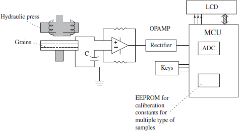
Figure 8.63 Prototype MCU based instrument interface circuit for measuring moisture in multiple type of grains

IR remote sensing control signals to a robot is that the ASCII code of the key that is pressed is sent serially by IR LED on-off radiation. The mode of sending is serial synchronous communication and is as follows. The code of the key remotely pressed precedes a synchronising character (for example, 0010 1101) or nibble (for example, 1101). The IR LED when bit = 1 current is on and when 1 is off.
A robot embeds the software at the kit having the MCU and interface circuit. Many times, the following features are required:
- Timers and library of timing functions.
- Four or six PWM channels.
- Interfaces of touch sensors, IR sensors, and motor proximity sensors.
- Remote infrared control bits serial synchronous communication interface.
- Remote as well as local serial I/O functions at the port pins.
- I/O lines for sharing with the external interfacing circuits.
Latest robots use the standard protocols like controller area network CAN. It incorporates distributed control using the CAN. Six standard servomotors drive the robot arm. It moves with ± 0.18° accuracy along the five axes (four for movement one for the gripper). The C505C microcontroller controls each of the six servomotors. The control is done using the PWM method. Pulses of width 1 ms to 2 ms are used every 20 ms for each servomotor. Each 1 ms pulse width is equal to −90° rotation and 2 ms is equal to 90° full rotation. It acts as a device (application) object in a distributed system controlled by the CAN bus. Latest robots use the wireless interfaces also. These are complex and perform the multiple functions. Recently, East Arizona State University built a LEGO MINDSTORMS robot (www.east.asu.edu/clas/dcst/Projects/March2004/VenkatramanaVishwanatham.pdf). It has a programmable control kit RCX employing 8051. It has for 3 sensors, 3 motors and IR serial communication interfaces. The interface examples of applications are (i) coin sorter robot, (ii) candy distributing robot (Fig. 8.65). (iii) automatic remote engine control and (iv) robotic toys.
Candy Distribrition Robot. There is a candy bowl with candy. A set of three incremental encoders note the rotation of motors M1, M2 and M3 in the mechanical assembly. A proximity sensor based on LED-FET detects child. Metal sensor guides the pick of candy from the bowl.
8.27 DIGITAL SIGNAL PROCESSING AND DIGITAL FILTERS
8.27.1 Digital Signal Processing (DSP)
DSP operations process the continuous signals and data. Many times, the operations are in real time. Many application examples are as follows: digital filters, motor control, voice recognition, synthesis of waveforms, waveform generation, spectrum analysis and pattern matching.
DSP and digital filtering need high arithmetic calculations performance. DSP operations need a MAC unit in the processor. MAC stands for multiply and accumulate. The coefficients are multiplied and accumulated in the sum for the desired number of terms in many expressions for DSP operations like digital filtering. These calculations have to be done fast. A DSP algorithm requires the sampling of the input at the discrete time interval. A Laplace transform determines the continuous time frequency response in a filter. The Z transform performs the discrete time transform, which needs the discrete samples of the input at successive intervals. Therefore, the algorithm requires a sum of products calculation, which needs the MAC functions.
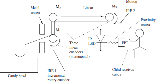
Figure 8.65 Robot System Design for Candy Distributing
Microcontroller 80296SA gives high performance (= 12.5 MIPS for DSP instructions and 16 MIPS for general-purpose instructions). Its features are as follows:
- The MAC unit executes a MAC in 80 ns using a 40-bit hardware accumulator. The 40-bit accumulator permits high precision in the arithmetic operations.
- High performance is achieved because of 50 MHz operations. External clock is of less frequency, a phase locked loop does the clock frequency multiplication in MCU internally.
- It has pipelined architecture and RISC instructions, which further improves the performance.
- Has 512 B register RAM (8051 has only 32 B) and 2 kB internal code/data RAM (8051 only 128 B).
- The address space is 6 MB. It permits a bigger code store after high level language compilation.
8.27.2 Digital Filters
Consider a digital filter that is linear and time invariant. The filter represented by a convolution equation for the outputy(n), given an arbitrary input x(n), is as follows:
where h(n) is the impulse response function of the filter. All the above functions are the complex functions. The convolution in the time domain means the multiplication in the frequency domain. Therefore, a Z transform simplifies the convolution into multiplications. The filter characteristic equation using the associated Z transforms gives the following equation:
The Y(z) and X(z) are polynomials. Now, these polynomials can be easily factored. This facilitates calculation of the factors by the MACs. Note that we call the roots of Y(z) = 0 as zeros of H(z) and the roots of X(z) as poles of H(z). The values of the zeros make the H(z) = 0 and the value of the poles make H(z) = œ (infinity).
Assume a filter that has all the zeros at the unit circle and all the poles always lie within the unit circle. Because the poles when outside the unit circle, means an unstable filter. Unstable filter means oscillations and ringing (repeated rising and falling frequency amplitudes) can occur.
FIR (finite impulse response) and IIR (infinite impulse response) filters: FIR (finite impulse response) and IIR (infinite impulse response) filters are two common digital filters. An FIR filter has greater stability than the IIR filter. The FIR output normally depends only on past inputs (not on past outputs). It can be easily conditioned to give response that is linear in phase.
The IIR filter on the other hand can be unstable and therefore gives a phase shift from the input to the output. The IIR output normally depends on the past outputs as well as past inputs that affect the present output. The IIR advantage is when the phase shift does not get affected. Then, less number of poles need to be calculated. Less execution time is needed because there is a smaller number of MAC operations in the IIR filter algorithm.
SUMMARY
- Key bounce problem is solved either by hardware latch or Schmitt trigger circuit at the input.
- Key bounce problem can also be solved by software. Scan line is first sent to 0 at the key. When the returned sensed input = 0 is read during a fixed period (~10 ms) five or ten times, 0 is finally accepted as the return line input and the key is taken as pressed.
- A keypad or keyboard is scanned by a number of output scan lines. The scan lines can be multiplexed through an encoder and may need to be decoded before the scan.
- A keyboard controller can perform all actions— encoding, decoding, debouncing and ASCII code conversion (using a lookup table in ROM) before sending the key information in the FIFO.
- The controller facilitates functions like N-key roll-over, two-key lockout and shift key and other keys detection before ASCII conversion.
- Software facilitates the smart use of the keys like in a mobile phone or TV remote control.
- Seven-segment LED displays are used for the hexadecimal digits. An annunciator LED or LCD display is used to display a fixed message with just two terminal input for glowing the 10% message.
- Alphanumeric displays are 16-segment displays. The LCD displays use very little power and multiplexed-LCD displays are used in handheld devices. Multi-line LCD matrix multiplexed displays are used in many devices.
- Dot matrix displays are used for alphanumeric as well as graphic displays. ROM addresses store the bytes for the pixels for each alphanumeric character to enable dot matrix displays from the ASCII coded inputs. A CGRAM address stores user defined graphics for a character or byte for a pixel.
- Programmable LCD display controller is used to display the user defined and ASCII codes characters on a multi-character multiline display.
- Touch screen interface uses a touch controller. The X and Y sense and drive lines are used to get inputs and LCD matrix displays the menu or virtual keypad.
- Intel 8279 is a programmable keyboard-cum-dis- play controller with debouncing and timing and logic circuit.
- A printer uses the RS232C serial port or Centronics parallel port.
- IEEE488 (GPIB) bus connects the instruments in listener and talker modes through the buses.
- Internal flash or EEPROM stores the codes, nonvolatile generated data and constant data and tables for the codes.
- Coils, relays and loudspeaker’s are interfaced using a power transistor and have a protection diode for induced transient high voltages.
- An optoisolator insulates the port pins of MCU from the interfacing motors, power devices, coils and relays.
- Music playing box has keypad interface as well as loudspeaker interface. Its embedded software enables paying of the stored music and practicing music notes playing.
- Stepper motor has a quad of coils. It moves in steps when it rotates. The stepwise movement is by shifting the currents from a coil(s) to another in a quad of coils using RL (rotate left) or RR (rotate right) instructions.
- IO modules with in-built optoisolators are used in interfacing the power devices to MCU.
- Interfacing circuit for a thermocouple is used for measuring temperatures.
- A servomotor control is by the control of width of pulse in PWM output.
- Optical rotatory and linear encoders are used for precision rotations and positioning.
- Industrial control interfaces use the IO modules, PWM outputs, timings and event processing features, remote and local sensor interfaces, remote and local actuator interfaces and ADCs.
KEY TERMS
16-Segment display. The use of which in the LED or LCD facilitates display of the alphanumeric characters.
7-Segment display : Use of which in the LEDs facilitates displaying hexadecimal digits.
Absolute encoder: An encoder for marking angular or linear position by the byte or bits obtained during either sationary or moving shaft or part position. It gives the position with greater precision if at a position the encoded bits are larger in number.
Actuator: A device to actuate the power or current or other output as per the control input voltage or current or frequency. For example, a furnace in which the resistance coil current actuates as per the DAC converted signal input. Loudspeaker is another example of an actuator.
Annunciator: Use of which in the LEDs or LCDs facilitates announcing a message of one or more characters, signs or logo or pictogram. Used in instruments to display units (for example, Volt) or parameter measured (for example, Frequency).
ASCII code: American Standard Code for Information Interchange is an international standard for sending the alphanumeric characters, special characters and control characters. Therefore, the keyboard and display interfaces also use this code.
Bounce: A spring bounces back and forth till the bounce effect annihilates (dies). A key when pressed or release also bounces. This effect on the observed voltage must be taken into account when reading a key.
CAN: Controller Area Network protocol based serial bus used in distributed control of the devices and systems. Used in connecting multiple robots in an industry. Used in an automobile for connecting multiple instruments and systems.
Capacitive sensor: A sensor in which capacitance changes detect a parameter, for example, proximity (say, paper) or moisture or humidity or level.
Centronics: A printer parallel interface standard for using the connector and handshaking signals.
Circular buffer: A FIFO buffer in which after the end the queue starts building from the start address. Useful in printer.
CNC: A machine for computer-based numeric control during operations of manufacturing involving latch, drilling and milling operations.
Coil: A circular winding of clockwise or anticlockwise turns to drive a motor or to create magnetic fields or sense the alternating magnetic fields. Used in motor or transformers or loudspeaker or relays.
Cursor: A display on the screen to show the current position or show select from a menu. The current poistion may be a current character position needing the input code for display. A cursor display may be continous or blinking.
Decoder. A circuit to activate one output out of many with the limited number of inputs. A 3 to 8 decoder has three input line and eight outputs the one among which activates as per the 3 bit input value. The input line is encoded. For example three encoded scan line activates one of the eight scan lines in the matrix of keys.
Digital filter. A filter using the DSP algorithms. The DSP operations use MAC unit(s) in the MCU.
Display matrix: A graph or logo or sign or picture or pictogram or character consists of horizontal and vertical pixels with pixel lighted or off as per the picture or character. A display matrix is the matrix to represnt a picture or character for display, the matrix elements 0 or 1 in the black-white or monocolour display. The display matrix element can be a nibble or byte in coloured displays.
Display RAM: A RAM to store the bytes or bits for a sequence of display outputs. RAM helps in refreshing the displays, which is required when only select units light up at an instance and we use the persistance of vision effect in the display.
Dot matrix: The dot matrix is the term used to represent a pixel with value = 0 or 1 by a dot. A dot print or dot display can be there or can be missing by inputs ‘1’ or ‘0’ corresponding to it.
ECG: Electrocardiogram, which records the heart beats and these reflect the soundness of the heart. The doctor analyses it for prescription.
Encoded track: A linear or rotatory track so that reading of the encoding gives the position on the track after decoding.
Erasing: A process of writing 1 or 1s at a byte-addresses or at a sector of bytes to enable writing the program or data later in an EEPROM or flash, respectively.
Event processor array: The events need to be processed in the control systems. An event appears by an edge transition or level transition at an input and event processing unit captures the instance at which the event occurs. An event may also be equality of the programmed time and system time and the event processing unit compares and raises a signal (like an alarm) or gives an output level or output transition. The event processing arrays use multiple event inputs and create multple output events. Event processor array is present in the certain advanced INTEL MCUs for control applications. It is similar to Motorola TPU (Timer Processing Unit).
FIFO RAM: A RAM to store the bytes or bits for a sequence of key-code input bytes or sensor inputs. RAM helps in reading in FIFO mode by an MCU or controller at its own time.
GPIB: General-Purpose Interface Bus from Hewlett Packard. Used to interface the data and handshaking signals between the instruments and devices having a GPIB controller. Also known as IEEE 488 bus.
Hall sensor: A sensor to sense the magnetic field by a popular effect known as Hall effect. [Refer text for the effect.]
IEEE 488: A GPIB bus.
IO module: A module to interface high current or volatge or power input to an MCU port or interface MCU port with the high power or current or voltage output(s).
IIR: Infinite Impulse Response.
Incremental encoder. An encoder for marking angular or linear displacement by the pulses obtained on moving by successive steps. In a moving part, it is used to note the displacements to a new position with respect to previous and index positions and is used to note the direction of motion and to note the current speed of motion.
IR remote control: Infrared Radiation from an LED at a remote location (few metres aways) is a method used in remote controls. The key pressed at the remote is ASCII coded and then the code is sent in synchrononous serial communciation by preceding sync character with the code.
Key: A key makes or breaks the contact by a push or other action. A key is used to send a character for a command or data intiating some action.
Keypad: A system consisting of up to ~ 16 keys for the human-computer or human and system interaction as in a telephone.
Keyboard: A system consisting of about 64 or more keys for the human-computer or human and system interaction as in computer.
LCD: Liquid Crystal Display used in calculators, instruments and handheld devices like mobile phone.
LCD controller: A programmable system for displaying the graphic and alphanumeric characters from the byte or ACSII inputs for data and commands.
Linear encoder: An encoder used to mark or record a linear position or displacement.
Linearity effect: Change in output y proportional to the change in the input x. y = a0 + a1x.
Listener. A term used when using a GPIB bus for the receiver of address or data on the bus.
Loadcell: A cell consisting of a mechanical assembly which is strained by the load such that the cell resistance gives the load on the cell.
Look-up table: A table in which a value at the cell directly gives the needed value, which corressponds to the key as per the given row and column. For example, a logarithmic table directly gives the value of log without intensive calculations for the input independent key (independent variable). For example, in a ROM, which stores the look-up table, the address is the input for a key or code or independent variable. The output stored after previous calculation is directly obtained on data bus when that address is the input and ROM is selected by the controller or MCU.
LVDT: Linear Variable Differential Transformer, it is a special device to note the changes in displacements from a natural position by noting the transformer output. [Output = 0 when displacement change is 0 with respect to a natural position.]
MAC: Multiply and Accumulate unit is a processor element used in finding the sum of a series consisting of the product terms. It is a must for the DSP calculations and in control system calculations.
Matrix: Used for the horizontal and vertical pixels or dots for graphics or alphanumeric characters, which is displayed or printed as per the pixels.
Multiplexed display: Display in which one channel is shown at one instance and another one at another instance. The display channels lights up sequentially and are cyclically refreshed for the display.
N-Key rollover, means that several keys in contact in quick succession or simultaneously and these can be read.
Non-linear effect: Change in output y not proportional to the change in the input x. y = a0 + a1x + a2x2 + …
Opto-isolating: Isolating one part of the circuit from the variations, induced and feedback effects at the other by using the optical system, for example, an LED- phototransistor pair.
Persistance of vision: A fact that eyes when shown units or fragments at intervals faster than 10 or 15 per second will sense these as continous units.
PLC: Programmable Logic Controller system to process the logical expressions and logic variables representing the switch or valve or solenoid positions in a plant or process for industrial control.
PWM: Pulse width modulation so that its duty cycle is the control input to a servomotor or DC motor. It is also used in DAC and generating controlled analog output.
Proximity sensor: A sensor to sense the approaching object in the vicinity.
Refreshing a display: Repeat cycle so that the same display is repeated more than 10 to 15 times (25 or 30 in case of TV) a second when using the multiplexed displays.
Repeat action keying: When a key is pressed for a duration longer than a specific period, it can be presumed to have been pressed repeatedly.
Robot: A mechatronics based assembly consisting of sensors, encoders and servo or DC or stepper motors to perform actions automatically and repeatedly (after suitably training the variables and program embedded into it), which otherwise needs human labour.
Rotatory encoder: An encoder to mark the angular positions during the rotations of a part.
Touch screen: LCD display with touch plate which enables graphic-user interactions using virtual keypad or menu. Touches are used to give inputs to the system.
Transducer: A device to produce and transfer a voltage or current or frequency as per the physical parameter or condition. Microphone is an example of transducer.
WFG: Wave Form Generator is an MCU feature in certain versions. It enables design of power inverters. It also enables certain power control applications.
Wheatstone Bridge: A bridge consisting for four arms. Consider a resistance-based bridge. A resistance each is placed in each arm. The bridge is given input between two corners and the output is noted between two remaining corners. The bridge is said to be balanced when the ratio of resistances in two arms equals the ratio in the other two arms. A sensing element resistance changes can be measured by the bridge. The unbalanced situation output directly reflects the change. Thermistor, loadcell, resistance thermometer employ the Wheatstone bridge circuit- based interface. Its maximum sensitivity is when all branches have equal values. The bridge can also be based on capacitances.
REVIEW QUESTIONS
- When do you need the interface circuit for application of microcontroller?
- When are the scan lines, encoded scan lines and return (sense) lines used? How many scan (encoded) lines and return lines will you need for a keyboard of 24 keys with 8 rows and 3 columns?
- What is the reason for the bounces in a key? When do you use the software debouncing routine when the hardware debounces the circuit? Show the circuits for both the cases.
- How does a parsing algorithm parse a key? Why do the parsed key input save in a FIFO as ASCII codes?
- How is an annunciator display the words like MHz, A.M., frequency or current?
- Why is a 16 segment arrangement used to display a character?
- How is an array of three segments having 24 LEDs used to display three hexadecimal digits by multiplexing and refreshing?
- (i) Explain dot matrix display. (ii) Explain functions of touch controller and software library for touch screen displays and inputs.
- Explain programming and interface for an LCD display controller which has two lines and sixteen characters in each line.
- Explain centronics parallel printer interface.
- Describe IEEE488 bus signals and timings.
- How can we rotate satellite dish axis at 45° from the present angular position using a microcontroller and a stepper motor? Design a suitable interface circuit and write appropriate codes for 8051. The motor step angle is 1.8° and currently the position is 0°.
- How can we rotate satellite dish axis at 45° from the present angular position using a microcontroller and a servomotor? Design a suitable interface circuit and write appropriate codes for 8051. The servomotor is at neutral when PWM pulse width =1.5 ms, at −90° when 1 ms and + 90° when 2 ms with pulse period = 30 ms.
- Explain the working of an optoisolator. Draw an interface circuit for isolating a triac in the 220 V AC line from a microcontroller pin port output.
- Explain control of a DC motor current and direction using internal PWM in an MCU.
- How can we use the incremental shaft angle encoder to measure the motor speed every second?
- How can we use the incremental shaft horizontal axis displacement encoder to find the shaft relative position?
- Describe method to interface a speaker in a music box.
- Describe how will you switch on and off four given solenoid valves in four tanks in a process. Use four port pins P1.0 to P1.3. Switch these cyclically after every 5 minutes.
- Explain the advantages of an optoisolator circuit. Describe how the optoisolators are used in interfacing the power devices to MCU.
- Describe a thermocouple interface.
- Describe use of Wheatstone bridge for measuring the temperature changes in a platinum resistance thermometer.
- Show a robot with four degrees of freedom. It consists of one stepper motor and three servomotors. How many are the PWM outputs and how many port bits are required? Show the necessary interfacing circuit.
- Explain process control. What are the units in the process control operations? What are the types of the logic operations required in the process controller?
- Describe how will you detect a nonmagnetic object in the proximity. Describe how you will detect a magnetic object in the proximity. How will you use a proximity sensor to measure the wind velocity? There are four cups, which rotate fast or slow as per wind speed and which rotate a spindle carrying an object detected by proximity sensor on each rotation.
- Explain basic interface requirements in an instrument for the car speed. How will you interface a transducer to an ADC device of MCU and generate measured output for an LCD unit?
- Describe the interfaces for the touch sensor, light sensor, motor proximity sensor and angular absolute position 17-bit encoder.
- Explain use of MAC unit, FIR filter and IIR filter.
PRACTICE EXERCISES
- Draw an interface for 3 scan (encoded) lines and 5 return lines in a keypad.
- Write an algorithm for sending ASCII codes in a FIFO repeatedly up to maximum 32 times when a key is pressed for a duration of more than 200 ms. The key is repeatedly parsed every 200 ms. Write 8051 assembly routine also.
- Write a part of a test algorithm. It detects if a key is stuck. If at the start on power-up a key is found to be in contact for more than 4 s, then the assumption will be that it is stuck. Write 8051 assembly routine also.
- Write an algorithm for an ASCII code for a key, which is smart. Smartness is as follows: When the key ‘0’ is pressed once, it is interpreted and coded for the number 0. When pressed the second time within 200 ms, interprets as ‘a ’, third time within next 200 ms as ‘b’, fourth time as ‘c’ and fifth time again as ‘0’. If the key at any instance is not pressed again within 200 ms, the code is confirmed and gives an ASCII code at the output for the key. [ASCII code for ‘0’ is 30H, ‘a’ 97H, ‘b’ 98H and ‘c’ 99H.] Write ‘C’ program or 8051 assembly routine also.
- Modify the above algorithm that if at the beginning the ‘#’ key was pressed before the ‘0’ key or a space key was pressed before the key or the ‘0’ key is pressed for the first time at the start then capital case for ‘a’ or ‘b’ or ‘c’ character will be selected at second or third or fourth contact, else the small case character as such will be selected. [ASCII code from ‘#’ key is 23H, space key is 20H and for the ‘A’ code is 65H, ‘B’ is 66H and ‘C’ is 99H.] Write ‘C’ program or 8051 assembly routine also.
- Draw a circuit for an array of 10 LED bars displaying the values, 0, 10, 20, 30, ..., 90 that correspond to car speed. Write 8051 assembly codes to glow the appropriate set of LEDs when interfaced to Port pins P1.0 to P1.3. Assume that the speed is stored in B register.
- There is a vertical bar of 4 LEDs showing room temperature during the four states, ‘very cool’, ‘cool’, ‘normal’ and ‘hot’. Draw the interfacing circuit and also write the 8051 algorithm for it.
- Tick the segments in Table 8.20 columns 3 to 11, which should glow to show a character in a 7-segment plus dot display unit. Write a byte in column 2 which should move to the port. The port pins 0 to 7 connect the a to h such that when the pin is at logic ‘0’ a segment glows. Use Fig. 8.10.
Table 8.20 Segment to glow for character display of 0,1,… 9.

- What are the segments that shall be lighted in a row of 16 LCD characters? Tick the correct cell in the Table 8.21 columns 1 to 17. [Hint: Use Fig. 8.12 for the position of a segment among the 16 segments in a digit.]
Table 8.21 Sixteen segments to glow for the characters

- There are 8 stepper motors with the motor identified by 3 bits P1.5, P1.6 and P1.7 and the coil currents are driven by Port Pins P1.0, P1.1, P1.2 and P1.3. Write an appropriate algorithm to move the fifth motor 10 steps.
- Write an 8051 assembly program to rotate a motor in half step. The stepper coils A, B, C, and D given the current cyclically at the successive instances T0 , T1 , T2 , to rotate in a direction during half step mode as in Table 8.22.
Table 8.22 Coil inputs at eight instances

- Search on the Web and make a table for finding the following:

- A transducer interfaces an ADC of an MCU and output to the LED display unit. The transducer generates 5 mV per kmph car speed in an automobile. Car speed lower limit = 0 kmph and upper limit = 120 kmph. The speed displays by four seven-segment LED display units and one annunciator.
- There is a MAC unit to multiply two thirty- two bit numbers and accumulate the result after addition with the previous result S into a sixty- four bit accumulator for S. How will you use it to sum ten terms in a series? S = a0.b9 + a1.b8 + a2.b7 + a3.b6 + a4.b5 + a5.b4 + a6.b3 + ab.b2 + a8.b1 + a9.b0. The coefficients ‘a’ store in block A and ‘a’ store in another block B. Write an appropriate algorithm.
MULTIPLE CHOICE QUESTIONS
- A key can be pressed _____ times in 10 s.
- 500
- 5000
- 50
- 100
Assume bounce can occur maximum 5 ms on pressing and 5 ms during release. Debouncing circuit timing is 10 ms.
- Consider a 4 rows × 4 columns keypad. The keys are numbered from 0 to F starting from the first row first column. There are two encoded scan lines from P1.0 and P1.1, which connect four rows of keys. [First row scans by output 00.] There are four columns and the return lines are also encoded and connect two port pins, P1.2 and P1.3. [First column connects by input 00. ] When key ‘F’ is pressed, the port P1.3-P1.2-P1.1 and P1.0 bits will be _____
- 0011
- 1100
- 1111
- 0000
- The FIFO RAM of a keyboard controller has ‘A’, ‘B’, ‘C’, ‘D’ and ‘E’ at an instance. It is read two times. Now ‘A’ is saved again. FIFO remaining bytes will be _____
- 41H and 42H
- 43H, 44H, 45H and 41H
- 41H, 43H, 44H and 45H
- 43H, 44H, 45H.
Assume ASCII coded saving
- A dot matrix display ROM stores the bit map for ‘A’ in seven bytes. The last byte will be _____
- 1000 0001
- 00010000
- 01000001
- 00001000
- Seven-segment LED display glows only vertical and middle segments only. The displayed character will be _____
- H
- B
- A
- E
- Sixteen-segment LCD display shows diagonal segments only. The displayed character will be _____
- X
- M or V
- Y
- X or V
- Intel 8279 can perform _____
- Consider four instructions after a reset and when an LCD controller (Hitachi 44780, Optrex DMC 16xx) RS pin connects P1.4, R/
 to P1.5 and E to P1.6.
- CLR C
- MOV P1.4, C
- MOV P1.5, C
- MOV P1.6, C;
- No action at the LCD controller
- Data and not the commands are written in LCD controller
- Command and not the data are written in LCD controller
- Display is cleared
- A printer uses a circular buffer of 1 kB. A page has 80 lines. Each line 78 characters, one control character for carriage return and one for new line. How many are the bytes, by which the buffer size should be increased so that each page can be stored in the buffer?
- 5 kB
- 2 kB
- 5536 bytes
- 5376 bytes
- IEEE488 (GPIB) bus has _____
- 16 lines
- 24 lines
- 18 lines
- 20 lines
- When do you need external fiash memory?
- When internal EPROM does not exist
- When internal fiash does not exist
- When a large amount of captured data is to be saved, which should be non-volatile
- Internal ROM does not exist
- Which of the statements is correct?
- A power transistor needs a protection diode across it for induced transient high voltages
- Solenoid valve need capacitor across it to protect from transients
- A solenoid valve coil needs a protection diode across it for induced transient high voltages
- An MCU port pins needs a protection diode across it for induced transient high voltages
- An optoisolator _____
- insulates the port pins of MCU
- insulates the inputs from the interfacing motors, power devices, coils and relays
- insulates the input from an output
- insulates the outputs from the power inputs
- Stepper motor moves one step angle when _____
- current is transferred from one coil to the neighboring coil
- current is switched off in the neighbouring coil
- current is switched on in the neighbouring coil
- when the current is given all the coils
- Interfacing ciruit for a thermocouple is used for measuring temperatures _____
- voltage developed is measured
- current developed is measured
- resistance is measured
- resistance change is measured by the MCU
- For a robot wrist, _____ is used.
- DC motor
- stepper motor
- servomotor
- induction motor
- An incremental rotatory encoder disc has 60 slots. At the index hole position of the disc the 8-bit counter-reading is 1111 1111. After moving 70 slots, the counter reading should become
- 0000 1001 or 1111 0101
- 0000 1010 or 1111 0100
- 0100 0110
- 0100 0100
- For industrial control _____
- An advanced EPA (Event Processor Array) structure, PWM, WFG and multi-channel on-chip ADC feature
- Input capture and out compare units
- Power IO
- An advanced EPA (Event Processor Array) structure, PWM and multi-channel on-chip ADC feature are must
- A 17-bit absolute angular position encoder gives angular resolution of _____
- 0.0002746°
- 0.002746°
- (1/17) °
- {1/(360*17}°
- A servomotor control uses _____.
- timers
- out compare features
- real time features
- PWM outputs
- A single touch screen _____.
- sends x and y coordinates of touched positions
- sends analog signal
- sends bits
- sends PWM inputs to touch screen controller
- A multi-touch screen senses by two touch finger gestures such as zoom in, zoom out and rotate using _____.
- touch-screen controller
- touch-screen controller, driver and library
- touch-screen controller and driver
- multi-touch library
FILL IN THE BLANKS TYPE QUESTIONS
- A key (switch) switch interfaces with port using _____. One signal is called _____, second called _____.
- An array of 16 keys can be scanned by _____ lines and _____ return lines in a keypad.
- A keyboard interface uses two pairs of _____ and _____ each for scan signals and return signals because there is _____ number of keys 16 when compared to the number of _____.
- LED _____ set or reset using individual _____ at _____ Port _____. It _____ or _____ when set or reset.
- When ASCII codes are used then character 0 is sent to serial port as _____, 1 as _____ , A as _____ and B as _____ and Space key is sent to serial port as _____
- _____ is sent to serial port as 48d (30H), _____ as 31H, _____ as 41H and _____ as 42H. Space key is sent to serial port as 20H.
- An LED has two ends, _____ and _____. An LED needs _____ mA during the ON state for the glow of LED. The _____ end of the LED connects the _____ supply through _____ Ohm and _____ end to a port pin.
- Multiplexing the _____ is done to display four hex-digits using 8- pins of a port. We can connect all the 8-segments of each hex-digit through a _____. At an instance only _____ hex-digit of 8-segment each _____.
- _____-segment LCD display can display (i) numeric and letters and (ii) both. It displays the letters, A to Z, and a to z.
- For a coloured display, in place each dot position will have _____ one red (R), second _____ (_____) and third _____ (_____). The colour of a pixel corresponds to combination of R_____, and _____ components.
- The port for the interfacing connect to _____ buses_____, _____, and _____ at the LCD controller.
- A touch-screen is an _____ device. It is used as a convenient alternative _____ or _____ . A touch screen is used in combination with a _____ system in mobile for graphic user interactions.
- The _____ are found between the two sets of lines are used to detect the touched (x, y) position on the screen when over the base there are conducting rectangular strips (layer 1). The strips form the electrodes directed along the X-axis.
- The 8279 is a programmable chip for various _____ and _____ control functions.
- A printer has following units _____, _____, _____ and _____ of the standard _____.
- An ADC selects channel number 03 when channel selects inputs are _____.