
7
System Design: Peripherals and Interfacing
Chapter Outline
- Understand important peripheral devices (8251,8255,8257,8259, ADC 0804, DAC 808) for the microprocessors and MCU-based system design
- Learn interfacing of peripherals
- Learn I2C bus for interfacing the systems
A microprocessor needs the external peripheral devices. The peripheral devices provide the parallel ports, serial ports, interrupt handling, direct memory access, ADC and DAC when they interface the microprocessor. An MCU possesses the many of the features of peripheral devices.
However, a particular MCU version in the family may not possess analog-to-digital converter, digital-to-analog converter, modem or DMA (direct memory access) or required device or control or interface circuit.
An MCU may have only a limited number of ports available than the required ones for an application. For example, 8051 in expanded mode has only eight or fewer bits of PI (Figure 3.4) available to interface other devices.
Because of the above reasons, it may be desired to interface 8051 to the external ports or peripheral device chips. The interfacing of peripherals enhances the capabilities of the given version in an MCU family for a specific application.
We shall learn in this chapter a few important peripherals. We will learn interfacing of these with the buses of microprocessor and MCU.
I2C serial bus finds many applications. We shall be learning that also.
7.1 SERIAL UART AND USART COMMUNICATION INTERFACES
Figures 7.1(a) and (b) show the serial bit formats in 8051 serial interface and in 8250 or 8251 peripheral IC chips.
7.1.1 Serial Interface in 8051
Serial interface shows that bytes receive and transmit in Universal asynchronous receiver and transmitter (UART) modes 1, 2 and 3. Mode 1 transmits and receives characters in (10-T) format. [one start bit plus 8-data bits and one stop bit in 10 time slots]. Figure 7.1(a) part 4 shows this format. Modes 2 and 3 transmit and receive in (11-T) format. [one start bit plus 8-data bits and one stop bit in 10 time slots].
The 8051 serial interface in mode 0 receives and transmits as shift register-based synchronous receiver and transmitter.
7.1.2 Serial UART Chip 8250
A modem [DCE (data communication equipment)] connects a COM port. The port is interfaced with Intel 8250 UART in a computer. 8250 is a serial communication chip. It finds extensive application for interfacing line driver and line receiver at COM port of an IBM PC. PC is called DTE (data terminal equipment) when it interfaces a DCE. The COM port of the PC interfaces to the modem or DCE.
The 8250 supports options of 5-bit, 6-bit, 7-bit and 8-bit per character (Figure 7.1(a)). It means, the data frame format is of 8T, 9T, 10T, and 11T where T is the reciprocal of the baud rate assuming 1 stop bit. The 8250 inserts one start bit before the character. It can insert one parity and one stop bit after the character bits (Figure 7.1(a) port 4 1, 2, 3 and 4). 8250 supports 1 or 2 or 1½ stop bit insertion. [Start bit means a logic 1 to 0 transition along with 0 for the period T. 1 stop bit means logic 1 for 1T interval, 2 stop bits for 2T and 1½ stop for 1½ T.] Figure 7.1(b) shows options for stop bits.
7.1.3 Serial USART Chip 8251
8051 synchronous-communication format is using the data and shift clock. There are two lines—one for the data and one for the clock. 8251 provides for only one line communication. It is programmable for both asynchronous UART like the 8250 as well as synchronous serial communication. Synchronisation at receiver end is done by synchronisation bits. (not by clock signals from transmitter.) 8251 inserts appropriate synchronization bits (or characters) in this mode. Intel USART 8251 is an enhanced featured chip. It is also a classic communication chip.
The following is a list of 8251 characteristics:
- Synchronous and asynchronous serial communication modes.
- Full-duplex transmission and reception. [Full duplex means send and receive both ways simultaneously.]
- Double buffered transmission and reception. [During reading and writing new character, the previous one is in the buffer.]
- Synchronous transmission or reception of 5 or 6 or 7 or 8 bits per character. Synchronous transmission or reception bit rate is settable between 0 and 64 kbps (kilo bit per s).
- Synchronization at the receiver is provided by insertion of a specific synchronization character (called sync character) or by the sync bits as the preceding characters before the data (Figure 7.1(c). Synchronization can be by internal or external sync character. The automatic sync-character insertion is programmable for one sync character or two.
Insertion can be of a single or double (two bytes or 16 bits) sync-character.
- Asynchronous transmission or reception of characters each of length 5 or 6 or 7 or 8 bits.
- Asynchronous transmission or reception with insertion of 1 or 2 or 1½ stop bit for each character.

Figure 7.1 (a) 5 Bit, 6 Bit, 7 Bit and 8 Bit Per Character Formats 1, 2, 3 and 4 at an UART Using the 8250/8251. 8051 Shows 8 Bit/character. An Additional Bit (P Bit) is also sent in Certain Modes. (b) 1 or 2 or 1 16 Stop Bit Insertion in 8250/8251 and (c) Synchronization Character (Called Sync-character) or Sync-bits as the Leading Characters Before the Data at USART 8251 Chip
- Baud rate for asynchronous transmission or reception is set by a clock. The clock frequency can be programmed as 64 or 16 or 1 times ofthe baud rate. Baud rate for asynchronous transmission or reception can be set between 0 and 19.2 K baud per s.
- Programmable by three ways—odd or even or none parity during an asynchronous mode.
- Automatic generation of break detection and break character.
- Parity, overrun and frame error detection.
- Input and outputs are at TTL levels. [2.8 V to 5 V logic 1 and 0 V to 0.8 V logic 0 at TTL output.]
Figure 7.2(a) shows a block diagram of the subunits at the 8251-chip. The block diagram gives an overview. It gives a preliminary understanding of the internal hardware. Figure 7.2(b) shows the signals and configuration of the pins at 8251-chip. Table 7.1 gives the meanings and uses of the subunits shown in the block diagram. Table 7.2 gives the uses of pins of 8251.

Figure 7.2 (a) Block Diagram of Subunits at 8251 and (b) Signals and Configuration of Pins at 8251
Table 7.1 The Meanings and Uses of the 8251 Subunits
| Subunits | Use |
|---|---|
Data bus buffer |
Internal buffer register on data bus—It holds the data byte from the data bus during write by the processor. It sends the byte to the data bus during the read operation. |
Transmit buffer (P-S) and receive buffer (S-P) |
Transmit buffer for sending data bits serially through TxD pin and receiver buffer for receiving the data serially through RxD pin. Start, parity and stop bits (or sync- characters during synchronous communication) are appended and detached at these buffers. TxD = 1 (mark) when the line is idle. |
Transmit control |
A transmitter-control subunit for generating the signal TxRDY (transmitter ready to receive data from processor for transmission) and TxEmpty transmitter empty (transmission of last bit completed)—connects to and from—TxC (transmitter clock), which controls the bit or baud rate of transmission. (TxRDY and RxRDY reset automatically on the processor write to the transmit buffer and processor read from the receive buffer). |
Receive control |
A receiver-control subunit generating the RxRDY (receiver ready for data read by the processor) and SynDet/BrkDet (on a sync-character or break-character detection)— connects to and from RxC (receiver clock), which controls the bit or baud rate of the synchronous or asynchronous reception. |
Read/write logic |
A read/write control logic with signals as follows. |
Modem control subunit |
This has four handshaking signals. Signals are as follows: |
a Figure 7.3 shows the interfacing circuit for 8251 with address and data buses of 80x86, 8051 or 68HC11; C/![]() (control/ data ) pin in 8251 connects A0 and the
(control/ data ) pin in 8251 connects A0 and the ![]() (chip-select) pin interfaces through a decoder to A1-A15. Figure 7.3 also shows connections of TTL level to RS232C level converter. Assume that F080 and F081H are the addresses chosen for the processor instructions for writing or reading at 8251. Table 7.3 gives the addresses for the 8251 communication interface. Decoding circuit is made such that when the processor sends any of these two addresses then the decoder output selects 8251 for read or write, then only CS = 0, else it is 1 for read or write other peripherals or memory addresses.
(chip-select) pin interfaces through a decoder to A1-A15. Figure 7.3 also shows connections of TTL level to RS232C level converter. Assume that F080 and F081H are the addresses chosen for the processor instructions for writing or reading at 8251. Table 7.3 gives the addresses for the 8251 communication interface. Decoding circuit is made such that when the processor sends any of these two addresses then the decoder output selects 8251 for read or write, then only CS = 0, else it is 1 for read or write other peripherals or memory addresses.

Firstly, the two addresses for the USART device are decided. Assume that these addresses are F080Hand F081H. The address bus A0 is directly connected to the chip. Upper 15 bits, A1 to A15 are common to both the addresses. Secondly A1-A15 are used for generating the ![]() signal for 8251.
signal for 8251.
- AD0-AD7 signals are used to latch A0-A7 using ALE.
- A0 connect to C/
 (control/ data ) pin in 8251.
 - Decoder circuit is designed such that when A15, A14, A13, A12 and A7 = 1s, A11, A10, A9, A8, A6, A5, A4, A3, A2 and A1 = 0s then a decoder output is 0 and connects the
 pin. The A1-A7 and A8-A15 connects to decoder circuit. The output of decoder selects the 8251 chip when the output connects to (chip select) pin in 8251.
 - D0-D7 bits connect to 8251 D0-D7 pins in 8251.
 and
and  (
( and
and  in 80x86) signals connect to and pins in 8251.
 ,
,  ,
,  and
and  pins in 8251 connect to RS232C port in computer. The port is called COM port. COM connects to modem (DCE). RS232C COM port has 9 or 25-pin connector.
- TxEmpty and RxRDY pins can be connected to the external interrupt pins of the processor.
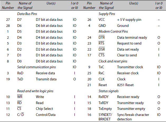
Table 7.3 Addresses and their uses for the 8251 Communication Interface When F080H and F081H are the Addresses Chosen for the Processor Instructions
| Direct Address | Use |
|---|---|
0xF080 |
Address for data transmission during write instruction at this address and for data reception during read by the processor instruction. The address is thus common for transmit buffer as well as receive buffer in 8251. |
0xF081 |
Address for sending the control words during write at this address, and for reading status bits by the processor instructions. This address is thus common for control words as well as status bytes for write and read at 8251. |
Two control words in asynchronous communication casea are sent in the following order after power up reset: (i) byte for mode instruction with b0 and b1 both not 0s and (ii) byte for the command instruction. The control words in synchronous communication caseb are sent in the following order after power up reset: (i) byte for mode instruction with b0 and b1 both 0s, (ii) byte for sync character to be used, (iii) another byte for second sync character if synchronous mode instruction resets the b7 = 0 and (iv) byte for the command instruction.
a Figure 7.4(a) shows the sequential order of sending control words after power on reset for 8251 programming for asynchronous communication.
b Figure 7.4(b) shows the sequential order of sending control words after power on reset for 8251 programming for synchronous communication with single or double sync character.

Figure 7.4 (a) Sequential Order of Sending Control Words After Power Reset for 8251 Programming for Asynchronous Communication and (b) Sequential Order of Sending Control Words After Power Reset for 8251 Programming for Synchronous Communication with Single or Double Sync Characters
7.1.4 Programming 8251
8251 is programmed y writing the control words for the mode and commands. However, there is only one address in 8251 when writing the words as well as for reading the status bits (byte) and for writing the mode and command words. A0 is 1 in the address and other bus signals A1-A15 in the address depend on how the chip connects to the address bus through a decoder. Assume that the 8251 data register and command word addresses are F080H and F081H, respectively. Then, during the move of a byte to F081H, A0 will be 1, C/ D pin is at 1 and A1-A15 decode accordingly to select the 8251. How can a single address be used for the various control words for the mode and command (control)? The chip is designed to provide this feature. It can be seen from the following.
- Any byte sent for the first time after the reset is interpreted as mode instruction.
- If mode instruction B1 and B2 (b0 and b1 bits) are 00, then the communication mode is a synchronous mode.
- (a) If mode instruction b0 and b1 bits are 10, then the communication mode is the asynchronous mode 1x. (b) If bits are 01, then the communication mode is an asynchronous mode 16x. (c) If bits are 11, then the communication mode is asynchronous mode 64x.
Note that 1x means communication rate and clocking rate are identical. 16x means communication rate is 16 times less than the clocking rate. 64x means communication rate is 64 times less than the clocking rate.
- If mode instruction is for asynchronous communication (B1 and B2 are not 00), then the following are the interpretations:
- (a) If mode instruction S2 and S1 bits meaning b7 and b6 bits (maximum and maximum but one significance bits) are 01, then the asynchronous communication mode is 1½ stop bit at the end. (b) If mode instruction b7 and b6 bits are 10, then the asynchronous communication mode is 1/ stop bit at the end. (c) If mode instruction b7 and b6 bits are 11, then the asynchronous communication mode is 2 stop bit at the end.
- If mode instruction EP bit b5 = 0, then parity generated is odd, else even. Parity generation enables only when if PEN bit b4 = 1.
- If mode instruction L2 and L1 bits (b3 and b2 bits) are 11, then the asynchronous communication character is of 8 bits, if 10, then 7 bits, if 01, then of 6 bits, and if 00, then of 5 bits.
- If mode instruction is for synchronous communication (B1 and B2 are 00), then the following are the interpretations: (a) If mode instruction L2 and L1 bits are 11, then the synchronous communication character is of 8 bits, if 10 then of 7 bits, if 01 then of 6 bits and if 00 then of 5 bits. (b) If mode instruction EP bit b5 = 0, then parity generated is odd, else even. Parity generation enables only when PEN bit b4 = 1. (c) If mode instruction ESD bit (b6) = 1, it means SYNDET is input and sync-character detection is from external device, else sync-character detection is internal and SYNDET is output. (d) If mode instruction SCS bit b7 = 1, it means after the mode instruction the next byte will be sent as control word and it will be the sync character to be used for synchronisation. (d) If mode instruction SCS bit b7 = 0, it means after the mode instruction the next two bytes will be sent as control words and there will be thus two sync characters to be used for synchronisation (bisync mode).
- If mode instruction is for synchronous communication (B1 and B2 are 00) then after the sync-character(s), the next byte will be interpreted as command instruction. If mode instruction is for asynchronous communication (B1 and B2 both are not 0s) then after the mode instruction (first one after reset), the next byte will be interpreted as the command instruction.
The mode instruction bits are interpreted as per Table 7.4.
Table 7.4 Meaning of Each Bit of Mode Instruction
| Bit Position | Name | Explanation of the Function |
|---|---|---|
(a) Asynchronous Mode |
||
b7 |
S2 |
= 0 means 1 stop bit mode asynchronous transmission provided S1 = 1 |
b6 |
S1 |
S2 and S1 = 00 invalid code |
b5 |
EP |
= 1 means even parity when PEN = 1 |
b4 |
PEN |
parity enable bit (see row above) |
b3 |
L2 |
= 0 means 5-bit per character mode communication provided L1 = 0 |
b2 |
L1 |
see row above |
b1 |
B2 |
= 0 means 1X mode asynchronous communication provided B1 = 1 |
b0 |
B1 |
see row above |
(b) Synchronous Mode |
||
b7 |
SCS |
= 1 means single sync-character after the character (of 8 or 7 or 6 or 5 bits) |
b6 |
ESD |
external sync-character detect |
b5 |
EP |
= 1 means even parity when PEN = 1 |
b4 |
PEN |
parity enable bit = 0 |
b3 |
L2 |
= 0 means 5-bit per character mode communication provided L1 = 0 |
b2 |
L1 |
see row above |
b1 |
B2 |
= 0 |
b0 |
B1 |
= 0 |
The command instruction bits are interpreted as per Table 7.5.
Table 7.5 Meaning of Each Bit of Command Instruction
| Bit Position | Name | Explanation of the Function |
|---|---|---|
b7 |
EH |
= 1, enter hunt mode and search for sync character. No meaning in asynchronous mode |
b6 |
IR |
internal reset |
b5 |
RTS |
= 1, request to send made to a DCE and thus make RTS pin 0 |
b4 |
ER |
error reset |
b3 |
SBK |
send break character |
b2 |
RxE |
= 1, enable receiver |
b1 |
DTR |
= 1, data terminal ready and make DTR pin 0 |
b0 |
TxEN |
= 1, enable transmitter |
Note: The status of the 8251 can be read using the same address used for writing the control words. Table 7.6 gives the meaning of each status bit.
Table 7.6 Meaning of Each Bit of Status Bits Read from the Address Identical to Control Word Address
| Bit Position | Name | Explanation of the Function |
|---|---|---|
b7 |
DSR |
= 1 means Data Set Ready and DSR pin has been forced 0 by the DCE. |
b6 |
SYNDET/BRKDET |
reflects 1 or 0 at the pin SYNDET/BRKDET |
b5 |
FE |
Frame error valid, stop bit not detected. It does not effect the operations otherwise (asynchronous case only) |
OE |
Overrun error (next character started at RxD before the processor read, the previously received one from the buffer). It does not affect the operations otherwise but previously overrun character at the receive buffer only affects |
|
b3 |
PE |
Parity error valid parity bit not detected. It does not affect the operations otherwise (parity enable case only) |
b2 |
TxEMPTY |
= 1 means transmitter empty. Further, TxRDY pin will also set = 1 when command bit TxEN = 1 and DCE signal CTS = 0 |
b1 |
RxRDY |
receiver ready; reflects 1 or 0 at the pin RxRDY |
b0 |
TxRDY |
Transmitter ready (byte sent by processor into transmit (Tx) buffer already transmitted and Tx buffer is empty). Further, TxEMPTY pin will also set = when command bit TxEN = 1 and DCE signal CTS = 0 as well as Tx buffer is empty. |
Example 7.1
- How will you write program instructions for 8251 for using the 8-bit data, even parity and one-stop bit UART mode? The mode is similar to the 8051 serial interface 11T mode with TB8 bit. Transmission is with a baud rate, which is 64th of clock rate.
- How will you write program instructions for using the 8-bit data, even parity and 1 byte sync-character = 11010010 in USRT mode? Set bit rate equal to clock frequency.
- How will you reprogram 8251 for using the 8-bit data, no parity and one-stop bit UART mode? This mode is similar to the 8051 serial interface 10T mode without TB8 bit transmission. Set baud rate 64th of clock frequency.
Assume the address of data buffer to be 0xF080 and of control words 0xF08l.
- Use Table 7.4(a) for the asynchronous mode. Consider the processor instructions just after the reset and for writing the mode and command words.
- First is mode write instruction. Store (move) 7FH [b5b4 = 11, b3b2 = 11, b1b0 = 11, b7 = 0 and b6 = 1] at address 0081H.
- After storing 7FH, the processor command instruction is write control word instruction for address 0081H. Use Table 7.5, store (move) 03H[b7 = 0, b6 = 0, b5 = 0, b4= 0, b3 = 0, b1= 1 and b0 = 1] at address 0081H.
Now, when the processor instruction writes a byte to 0080H, the byte transmits as I-start bit, 8-bit data, even parity bit and I-stop bit UART mode with baud rate in 64X clock mode.
- Use Table 7.4(b) for the synchronous mode. For programming 8251 after the reset, the processor will write the following mode, sync-char and command instructions:
- Store (move) 0BAH [b7 = 1, b6 = 0, b5 = 1, b4 = 1, b3b2 = 11, b1b0 = 00] at address 0081H.
- After the mode instruction, next write will be the sync character at 0081H. Store (move) 0D2H.
- After the sync character, next will be the command instruction at 0081H. Store (move) 03H [b7 = 0, b6 = 0, b5 = 0, b4 = 0, b3 = 0, b1 = 1 and b0 = 1] at address 0081H.
Now, when the processor instruction writes a byte to 0080H, it will be transmitted as sync character before 8-bit data with bit rate as per TxC clock rate.
- Assume a 8251 has been programmed by writing control words. Use Table 7.5 for internal reset. Reprogramming is done after the internal reset of 8251. We program the processor to write the following command instruction for internal reset:
- Store (move) 40H [b6 = 1, all other bits do not matter] at address 081H.
- After the reset command instruction, next write will be for mode instruction at 0081H (Table 7.4(a)). Store (move) 4FH [b4 = 0, b3b2 = 11, b1b0 = 11, b7 = 0 b6 = 1 and b5 can be 1 or 0] at address 0081H.
- After it, the processor will send the command instruction to address 0081H (Table 7.5). Store (move) 03H [b7 = 0, b6 = 0, b5 = 0, b4= 0, b3 = 0, b1= 1 and b0 = 1] at address 0081H.
Now, when the processor instruction writes a byte to 0080H, it will be transmitted by 8251 as UART start bit plus 8-bit data plus 1 stop bit with baud rate as per (1/64) of TxC clock rate.
Example 7.2
Assume addresses of data buffer and control words = FF80H and FF81H. How will you find the status of 8251?
Status bits are read using the same address as control words address. Using Table 7.6, we interpret the meaning of each bit.
7.1.5 Interfacing to Processor and DCE
Processor connects the 8251 using the circuit shown in Figure 7.3. RxD and TxD pins of 8251 pins are at the TTL levels of voltages. Using an appropriate TTL to RS232C and vice versa converter, the 8251 connects to a PC (DTE). Figure 7.3 shows connections between the converter and 8251. DTE COM port 9 pin connector connects to DCE. Now consider interfacing between 8251 and DCE. SYNDET pin is connected to an external device for sending synchronous character. Figure 7.5(a) shows this. Mode instruction is programmed after reset of b6 to 0. The SYNDET/BRKDET pin is connected to a synchronous modem device, as shown in Figure 7.5(b). Mode instruction sets b6 to 1.
When external baud rate generator is used, SYNC device connects to RxC and TxC.
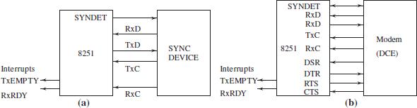
Figure 7.5 (a) The SYNDET is Connected to an External Device for Sending Synchronous Character and (b) The SYNDET Connection to a Synchronous Modem Device
7.2 PARALLEL IO PORTS INTERFACE 8255
When the 8051 is used in the expanded mode, only P1 or its few pins are available for the port operations. Consider the following needs:
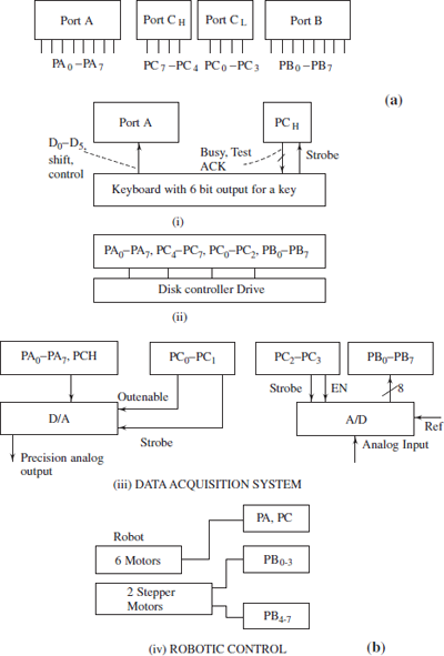
- Port operations are needed, for example, when interfacing a stepper motor. Stepper motor needs four bits. A robot with four stepper motors (one for the waist, one for the hand, one for the elbow and one for the wrist) will need four four-bit port. Total 16 bits at port will be required for interfacing 4 motors. Figure 7.6(a) shows three ports used as two ports of eight bits each and two ports for four bits each. Figure 7.6(b) shows four exemplary applications.
- Assume a system with up to eight subsystems (or subunits). An example is the system with up to eight LEDs or display systems. Another example is a robot with eight degrees of freedom with one DC motor each for movement in each degree of freedom. A complex example is a plant with temperature and pressure controls at the different chambers. Each subunit is to be programmed for either 1 or 0 independently by the direct bit set or reset. It needs eight one-bit ports. Figure 7.7(a) shows an 8-bit port as the eight one-bit ports when we use a direct set-reset mode. Figure 7.7(b) shows the three applications.

Figure 7.7 (a) Eight-bit Port as the Eight One-bit Ports in Direct Set-Reset Mode and (b) Three Application Examples
- Consider an external peripheral like a keypad that strobes the information about the key out of the eight keys pressed at an instant (Figure 7.8(a)). Three handshaking signals (strobe, acknowledge and interrupt) are used along with an input port. This enables an external peripheral to send the bytes. The bytes are sent to input port in interrupt-driven mode (Section 7.3.1(2)).
- Consider 3 signals—Two handshaking and one interrupt control signals (out-buffer full, acknowledge and interrupt); Figure 7.8(b) shows a circuit at an output port to enable an external peripheral to receive the bytes in interrupt-driven mode. The external peripheral may be a printer. Only two signals connect the external peripheral in case of the interrupt is internally used by processor which interfaces the port. PC3 or PC0 connects either to external peripheral interrupt input or to the processor interrupt input.
- Four handshaking signals and one interrupt control signal (Figures 7.8(c) and (d)) are used at an input-output bi-directional port. This enables an external peripheral to receive and send the bytes in interrupt-driven mode (Section 7.3.1(2)). The external peripheral may be disk controller. It needs one interrupt, two for input mode handshaking and two for output mode handshaking.
Programmable peripheral interface (PPI) Intel 8255 is an industry standard chip. It provides the needed interfacing circuitry, particularly to Intel family processors. It is used for many applications.

Figure 7.8 (a) An Input Port with Two Handshaking and One Interrupt Control Signal, (b) An Output Port with Two Handshaking and One Interrupt Control Signal. (c) Bidirectional Input Output Port with Four Handshaking and One Interrupt Control Signal and (d) Application Example
8255 has the following capabilities:
- Supports to three ports (24 programmable I/O lines)—two eight bit and two four bits each, ports programmable as input as well as output (Figure 7.6(a)).
- Supports a port as eight one-bit ports in the direct bit set-reset mode (Figure 7.7(b)).
- Support to the input port with two handshaking and interrupt-control signals (Figure 7.8(a)) and the output port with two handshaking and an interrupt control signal (Figure 7.8(b)).
- Support to a bi-directional input-output port with four handshaking and one interrupt control signal (Figure 7.8(c)).
- It has TTL level inputs and outputs compatibility. It has compatibility with the buses of Intel processor families.
Figure 7.9(a) shows block diagram of subunits in 8255. The block diagram gives an overview of the internal hardware. Figure 7.9(b) shows the signals and configuration of the pins at the 8255 chip. 8255 is a programmable chip.

Figure 7.9 (a) The Block Diagram of Subunits at 8255 and (b) Signals and Configuration of Pins at 8255
- There are 24 port pins. These are programmed in two groups—Group A consists of 8 bits of port A (PA0-PA7) and 4 bits (upper) of port C (PC4-PC7). Group B consists of 8 bits of port B (PB0-PB7) and 4 bits (lower) of port C (PC0-PC3).
- A group is programmed in three major modes of operations—mode 0, mode 1 and mode 2. The A, B and ports as well as the control instruction for the operational mode has four distinct addresses in 8255. Thus, there are four addresses for an 8255 that used by instructions of the processor.
- 8255 is a written data byte which latches at the port using the processor write instruction for write of data buffer. The latching is at the addressed port. The 8255 reads the latched data byte. The processor uses read instruction for the read of data buffer. The reading of the latched byte is from the addressed port.
- 8255 reads Port C status bits (byte) by processor read instructions for the status of pins of Port C. PC status bits are read when these pins are used for the handshaking and interrupt control.
- Mode bits written earlier can be read back from the same address as for writing the mode word.
Programming aspects of 8255 are described in Section 7.2.1. Programming must follow the reset on power-up. 8255 once programmed by writing just one byte control word only (for the mode instruction), it will continue to work as programmed till power-down or till reprogrammed by writing a fresh set of control bits.
Table 7.7 gives the meanings and use of the subunits shown in the block diagram. Table 7.8 will give the meanings and uses of each pin.
Table 7.7 The Meaning and Use of the Subunits Shown in the Block Diagram of 8255
| Full Form | Use |
|---|---|
Data bus data buffer |
An internal buffer register connects the data bus. Buffer holds the data byte from the bus during write and sends the byte to data bus during read operations of processor. Writing can be at any of the four addresses: three for the ports and one for control word. |
Group A Port A, Group A Port C upper, Group B Port C lower and Group B Port B |
These correspond to 24 pins for the ports. Ports are called PA, PCH (PC upper), PCL (PC lower) and PB, respectively. |
Group A control |
Group A control subunit for controlling Group A pin operations as per the mode word programmed for the modes |
Group B control |
Group B control subunit for controlling Group B pin operations as per the mode word programmed for mode control |
Read/write control logic |
Read/write control logic signals are as follows: (a) Reset (to reset control logic of 8255), connects to reset-out at processor pin, (b) |
a Figure 7.10 shows the interfacing of 8255 with 80x86, 8051 or 68HC11 address and data buses: (A1, A0) connections and ![]() (chip select) connecting to A2-A15 through a decoder. Table 7.9 gives the addresses for the 8255 when 40H, 41H, 42H and 43H are the chosen addresses which are used by the processor for writing or reading at PA, PB, PC and mode control. Decoding circuit is such that when the processor addresses 8255 for read or write, then only
(chip select) connecting to A2-A15 through a decoder. Table 7.9 gives the addresses for the 8255 when 40H, 41H, 42H and 43H are the chosen addresses which are used by the processor for writing or reading at PA, PB, PC and mode control. Decoding circuit is such that when the processor addresses 8255 for read or write, then only ![]() = 0, else 1 when addressing other peripherals or memory addresses.
= 0, else 1 when addressing other peripherals or memory addresses.
Table 7.8 Pins in 8255

a = 1 or 0 (When A1 and A0 are both 1 then for mode control).
b Also used for the handshaking and interrupt-control signals.
Table 7.9 Example Addresses Chosen for 8255 PPI for Design of Decoding Circuit
| Direct Address | Explanation of the Function |
|---|---|
40H |
Port A |
41H |
Port B |
42H |
Port C |
43H |
(i) For sending the mode words (when b7 = 1) then during write and (ii) for mode bits read by processor instructions. (iii) When maximum significant bit b7 in word is, written = 0 then is commanded for set or reset of one of the bits at PC. |
7.2.1 Programming 8255
8255 programs by writing eight control word bits at the mode (command) address. The control byte is interpreted as the mode when b7 = 1 (b7 is the maximum significant bit sent by the processor) else is interpreted as control word for the port C pin.
The mode instruction bits are interpreted as in Table 7.10. Mode 0 for Group A or B means that the group main port (A or B) operation is without handshaking signal. Mode 1 for a Group A or B means that group main port A or B operation is with the handshaking and interrupt signal (Figures 7.8(a) and (b)). Mode 2 for a Group A means that group main port A operation to the external peripheral is bidirectional with the four handshaking and one interrupt signals (Figures 7.8(c)). [Bi-directional means Port A and associated PC bits are not specifically defined as input only or output only. Bit b4 of mode write instruction is redundant.]

Figure 7.10 Interfacing 8255 Chip With Address and Data Buses of 8085 or 80x86, 8051 or 68HC11; A0 and A1 Connect to A1 and A0 of Address Bus and CS (Chip-Select) Connects to A2-A15 or A2 to A7 (for 8-bit Port Address) Through a Decoder. IO/M , RD and WR Used in 8085
Table 7.10 Meaning of Each Bit of Mode Instruction (b7 Not 0)
The Port C bits direct set-reset instruction bits are interpreted as given in Table 7.11.
Table 7.11 Meaning of Each Bit of Set-Reset Instruction for Port C Bits
| Bit Position | Explanation of the Function |
|---|---|
b7 |
= 0, Port C bits direct set-reset instruction active |
b6, b5 and b4 |
May be 1 or 0 |
b3, b2 and b1 |
= 111 means PC7; = 110, PC6; = 101, PC5; = 100, PC4; = 011, PC3; =0101, PC2; = 001, PC1; = 000, PC0 |
b0 |
= 1,set |
a When b7 of control word = 0.
Table 7.12 (a) Status of the 8255 PA, PB and PC Pins in Mode 0
| Pins | Function |
|---|---|
PA0-PA7 |
Input or output (as per b4 mode write instruction) 8-bit port when Group A mode 0 |
PC4-PC7 |
Input or output (as per b3 mode write instruction) 4-bit port when Group A mode 0 |
PB0-PB7 |
Input or output (as per b1 mode write instruction) 8-bit port when Group B mode 0 |
PC0-PC3 |
Input or output (as per b0 mode write instruction) 4-bit port when Group B mode 0 |
(b) Status of the 8255 PA, PB and PC Pins in Group A Mode 1 and Group B Mode 1
(c) Status of the 8255 PA and PC Pins in Group A Mode 2
| Pins | Mode 2 Group | Function |
|---|---|---|
PC3 |
Group A |
Interrupt control signal to processor for port A |
PC7 |
Group A |
Output signal |
PC6 |
Group A |
Input signal |
PC5 |
Group A |
Output signal |
PC4 |
Group A |
Input signal |
Note: Remaining bits of PC, which are not used for the handshaking or interrupt control are usable in the same manner as in mode 0 Group B or A.
Let us assume that in the following examples, 8255 is interfaced to the processor buses such that it is addressed using the addresses given in Table 7.9.
Example 7.3
- How do we program 8255 for 8-bit data output to port A and 8-bit input at port B pins? Assume no handshaking or interrupt signals are used at each of these ports.
- How do we program the 8255 for (i) 8-bit data input to port A with two handshaking and one interrupt signals and (ii) 8-bit input at port B pins with no handshaking or interrupt signals? Assume that mode instruction address 43H is as per Table 7.9.
- Use Table 7.10. After resetting the processor, an instruction should write the following mode instruction:
- Store (move) 82H (b7 = I for mode activate, b6b5 = 00 for mode 0 Group A, b4 = 0 for port A output b2 = 0, bI = I for Port B input) at address 43H.
- Store a byte from accumulator to 40H for Port A write.
- Load a byte to accumulator from 4IH for Port B read.
- After processor reset, store 0B2H at 43H to program.
Example 7.4
(i) How will you reset PC3? Assume PC3 connects an interface to a valve. (ii) How will you set PC0? Assume PC3 connects to an LED circuit.
(i) Store 06H at control word address 43H direct bit set-reset instruction. This makes b7 = 0, b3b2b1 = 011, and b0 = 0 and therefore, PC3 resets to 0, and (ii) Store 01H at control word address 43H direct bit set-reset instruction. This makes b7 = 0, b3b2b1 = 000, and b0 = 1 and therefore, PC0 sets to 1.
7.2.2 Interfacing 8255 to Processor
Firstly, four addresses for 8255 are chosen. Let us assume that these addresses are 40H, 41H, 42H and 43H. Upper 14 bits A2 to A15 are common to all four addresses. Hence, these are used for generating the ![]() signal for 8255. Decoder circuit is designed in such a way that when A7, A6, A5, A4, A3 = 0s and A2 = 1 the decoder output is equal to 0 and connects
signal for 8255. Decoder circuit is designed in such a way that when A7, A6, A5, A4, A3 = 0s and A2 = 1 the decoder output is equal to 0 and connects ![]() pin.
pin.
Figure 7.10 showed the interfacing of the 8255 chip with address and data buses of processor (such as 8085 or 80x86, 8051 or 68HC11), A0 and A1 connecting to A0 and A1 bus signals and ![]() (chip-select) is from a decoding circuit. Decoding circuit decodes A2-A15 or A2-A7 (or A10-A15 in case of 8085) bus signals and sends
(chip-select) is from a decoding circuit. Decoding circuit decodes A2-A15 or A2-A7 (or A10-A15 in case of 8085) bus signals and sends ![]() when address bus addresses any of the address among 40H, 41H, 42H and 43H.
when address bus addresses any of the address among 40H, 41H, 42H and 43H.
- When AD0-AD7 are the signals, using ALE at the processor, the address A0-A7 bus signals are latched before decoding. Address bus signals A0-A1 after latching are connected to the chip A0 and A1 pins.
- D0-D7 bus signals connect to 8255 D0-D7 pins (Table 7.8).
- and (IORD and in 80x86) signals connect to and pins of 8255. Reset pin connects the reset out pin of the processor.
7.3 DMA CONTROLLER 8257
7.3.1 Methods for IO Transactions
Assume that IO transactions take place between the peripheral device and system-memory. Peripheral needs to send data into the system memory or receive data from the memory.
Consider the following:
- A peripheral like a hard disk needs to load the program or file into the memory. It needs bulk (1 kB plus) transfer and there is need of large number of IO transactions between memory and disk. Alternatively, a file is to be written into the disk. It needs bulk (1 kB plus) transfer and there is need for large number of the transactions.
- A memory location needs to be read and rewritten at the same location again and again because memory happens to be DRAM (dynamic RAM) and RAM needs refreshing within a specified interval.
There are three methods for the IO transactions which occur between peripheral device and system (Figures 7.11(a), (b) and (c)).
- Programmed IO transfer (busy and wait IO) mode
- Read: A byte or word is read using an instruction. Then wait is done for the period in which the next byte or word will be available and then transfer that by the read instruction when ready. Continue wait and transfer till all the bytes are transferred as programmed.
- Write: A byte or word is written using a processor instruction. Wait for the period within which next byte or word can be written into the peripheral and then again transfer the byte or words using the processor write instruction when ready. Continue till all the bytes are transferred as programmed (Figure 7.11(a)).
The method is therefore, also called busy and wait IO method. The 8255 mode 0, Group A or B transactions are the busy and wait IO mode transfers. Note: a status flag will show when the peripheral is ready for a next read or write operation.
- Interrupt-driven IO transfer mode
- Read: A byte or word is read using a processor instruction on an interrupt using an ISR. Wait for the next interrupt and till then execution of the foreground program continue or other tasks run. Read on next ISR call on interrupt.
- Write: A byte or word is written using a processor instruction on an interrupt using an ISR. Wait for the next interrupt and till then perform other tasks or continue the foreground program. Write on the next ISR run on the next interrupt (Figure 7.11(b)). The 8255 mode 1 Group A or B or mode 2 Group A transactions are data transfers interrupt-driven IO mode.
- Direct memory access (DMA) by DMAC
- Read: A byte or word is read from the peripheral not by using a processor instruction but by using a DMAC (DMA controller), which transfers it to the memory at address block. A block of addresses is programmed for data transfer using direct memory (RAM) access. The method is such that processor do not wait for input port to be ready. The method is also such that processor do not wait for completion of output. DMAC sends a hold request and processor acknowledging as and when the processor buses are available to DMAC. Transfers do not use the processor instructions and fetches from peripheral during read instructions. DMAC continues to read and transfer to the memory till the programmed number of bytes is transferred. After the transfer is complete, it interrupts the processor so that the processor can reprogram the DMAC.

Figure 7.11 (a) Programmed IO (Bus-wait IO) Transfer Mode, (b) Interrupt-driven IO Transfer Mode and (c) Direct Memory Access by DMAC (Peripheral Transactions Server (PTS)) Driven IO Transfer Mode
The method is such that processor programs only once by sending (i) instructions to the DMAC, (ii) start address of the memory and the programmed number of bytes, which are to be transferred. The processor continues other tasks and waits for the ISR run on interrupt from DMAC after the terminal last byte is transferred from the peripheral.
- Write: A byte or word is sent to the peripheral not by using a processor write instruction but by the DMAC, which transfers it from the memory (at a programmed address block). Transfer is by DMAC sending a hold request and processor acknowledging as and when the processor buses are available to it. Transfers do not use the processor using the write instructions. DMAC follows the course as described above. The method is such that processor programs the DMAC once. The processor continues other tasks till requisite number of bytes are transmitted during idle state of the buses.
- Read: A byte or word is read from the peripheral not by using a processor instruction but by using a DMAC (DMA controller), which transfers it to the memory at address block. A block of addresses is programmed for data transfer using direct memory (RAM) access. The method is such that processor do not wait for input port to be ready. The method is also such that processor do not wait for completion of output. DMAC sends a hold request and processor acknowledging as and when the processor buses are available to DMAC. Transfers do not use the processor instructions and fetches from peripheral during read instructions. DMAC continues to read and transfer to the memory till the programmed number of bytes is transferred. After the transfer is complete, it interrupts the processor so that the processor can reprogram the DMAC.
When the transfer completes, the processor is interrupted. Processor then takes further step as required. A DMAC is a PTS (peripheral transactions server), which reduces the need of running of an ISR for each byte or word transfer. A context switch to ISR and return switch from ISR takes many cycles. The method of using PTS is such that Processor just initialises the DMAC by running a few instructions to send the data in registers and commands (sends start address, count-value and mode instruction). The ISR runs on terminal count in the end only.
DMAC is the most efficient way of using the idle time of processor buses. It is used for the bulk transfers in between the memory and peripheral when required. Figure 7.11(c) shows the block diagram, signals and buses when using a DMAC.
A multi-channel DMAC facilitates transactions with several peripherals. For example, a four channel DMAC can perform transactions with the floppy and hard disks as well as DRAM refresh controller in a computer.
The 8051 does not facilitate use of DMA. 8257 is Intel DMAC chip for the same. Several MCU family versions provide the on-chip PTS (single channel or multiple channels). 80196 MCU has built-in PTS device (DMAC). 80960 MCU has built-in PTS device for DMAC as well as IOP (input-output processor).
Programmable direct memory access controller (DMAC) Intel 8257 is for the much needed DMA transactions, particularly suited to Intel family processors in the computers as well as for many applications.
The 8257 DMAC has the following capabilities:
- It supports four channels.
- Priority DMA requests control logic exits so that higher priority peripheral transaction channel can transfer with higher priority and a channel can also be inhibited.
- Output on each terminal count (after last DMA-byte transaction) as well as after each completion of the 128 transactions.
- Facilitates auto load, (of DMAC registers) after the last byte transfer.
- TTL level inputs and outputs compatibility and a compatibility with the buses of the Intel processor families.
The 8257 is a programmable chip. It can be commanded to transfer a maximum of 16 kB data between the memory and peripheral device without further processor instructions. There are four bidirectional address pins A0-A3 and four unidirectional address pins A4-A7 and 8-data bus pins D0-D7. A0-A7 thus outputs LSB (least significant byte) for address for the memory. It outputs MSB (maximum significant byte) to the memory through a decoder 8212 using the D0-D7 lines (8212 decoding is similar to decoding of AD0-AD7 by a latch using the ALE). For each channel there is a separate 16-bit terminal count register. For each channel there is a separate 16- bit DMA address register. The 8257 channels generate DACK0, DACK1, DACK2 and DACK3 active 0 signals to the peripherals, when these request the DMA transactions through DRQ0, DRQ1, DRQ2 and DRQ3 active 1 signals.
7.3.2 Programming 8257
Once the 8257 is programmed, the IO transactions using DMA can take place. 8257 chip is assigned 16 addresses using which the processor can write chip internal registers and MODESET register (for mode instruction).
Each channel has one 16-bit register for ADDR [DMA address (start address for read or write at RAM) and one 16-bit register for TC [terminal count (number of bytes to be transferred)] using DMA transactions. It should be noted that the 16-bit register has the same address for LSB and MSB. Whatever byte is written first by processor instruction is presumed as LSB and whatever next as MSB. Next to MSB the next write will be accepted as LSB. These are loaded for initialising the DMAC using A0-A3.
When A0-A3 are inputs to DMAC and A3 = 0, one of the above 8257 internal registers selects when these are written or read by the processor (or master) (Ch0 DMA address = 0000; Ch0 TC address = 0001; Ch1 DMA address = 0010; Ch0 TC address = 0011;…). When A3 = 1, in place of the above internal registers, the MODE SET register is selected. It is programmed (written) after all the TCs and DMA addresses are written. When A3 = 1 and the 8257 is read, then the status register is selected. Table 7.13 gives the meaning of the bits at the MODESET and status register.
Table 7.13 (a) Meaning of Each Bit of Mode Instruction at Mode Set Registera
a Accessed or written from address with A3A2A1A0 = 1000, must be written on 8257 reset to activate DMAC transactions.
b A DMAC channel starts transactions after enabling the channel.
(b) Meaning of Each Byte Sent (or read) into Internal Registersa
| Address Bits | Function When 8257 is Addressed at that Address |
|---|---|
0000 |
Ch0 DMA Address 16-bit register |
0001 |
Ch0 TC 16-bit register |
0010 |
Ch1 DMA Address 16-bit register |
0011 |
Ch1 TC16-bit register |
0100 |
Ch2 DMA Address 16-bit register |
0101 |
Ch2 TC16-bit register |
0110 |
Ch3 DMA Address 16-bit register |
0111 |
Ch3 TC 16-bit register |
1000 |
Mode Set 8-bit register (when written) and Status register 8-bit when read |
(c) Meaning of Each Bit of Status Register (Accessed/read From Address with A3A2A1A0 = 1000)
| Bit position | Function |
|---|---|
b7 |
= 0 (always reset) |
b6 |
= 0 (always reset) |
b5 |
= 0 (always reset) |
b4 |
= 1, update flag (No effect of status register read instruction)a |
b3 |
= 1, Ch3 TC output activated, after reaching 0b |
b2 |
= 1, Ch2 TC output activated after reaching 0b |
b1 |
= 1, Ch1 TC output activated after reaching 0b |
b0 |
= 1, Ch0 TC output activated after reaching 0b |
a When update flag = 1 then the processor instruction should not overwrite the internal registers if updating is in progress for them.
b Remains 1 till the status register is read, after that it automatically resets to 0. It resets to 0 on 8257 reset also.
Figure 7.12(a) shows the block diagram of the subunits at 8257 chip. The block diagram gives a simple overview (for a preliminary understanding) of the internal hardware. Figure 7.12(b) shows the signals and configuration of the pins at the 8257 chip.

Figure 7.12 (a) Block Diagram of Subunits at 8257 and (b) Signals and uses of the Pins at 8257
Table 7.14 gives the meaning and use of each subunit shown in the block diagram.
Table 7.14 The Meaning and Use of the Subunits Shown in 8257 Block Diagram
| Subunits | Use |
|---|---|
Data bus buffer |
Internal buffer register for the data bus. It holds data byte from the data bus or the address A8-A15. |
Control logic and mode setting |
It sends HRQ (hold request) to the processor to get access to the buses and processor grants that request through HLDA (hold acknowledge). It issues terminal count (TC) signal to processor, at which processor can interrupt and run an ISR to modify DMAC program or stop further DMAC use. It also issues mark signal after each 128th cycle also. It sends A4-A7 address signals to the memory along with the A0-A3 by read-write logic and along with the A8-A15 using D0-D7 lines. It sends MEMR and MEMW signals to memory for memory-read and memory-write. It sends ADSTB (address strobe) signal so that 8212 or other decoder can latch A8-A15 from the D0-D7 lines. It sends AEN (address enable) to disable system data bus or inhibit other peripherals not attached to the DMAC to send the address. Ready signal to the logic extends a read or write cycle in case the memory chip needs longer cycles for a transaction. |
Priority resolver |
To resolve the priorities as per the program written at the 8257 register for mode instruction |
Ch0 Address/counter |
For channel 0 memory start address and counts (programmed number of bytes for the transfer before DMAC issues TC signal) |
Ch1 Address/counter |
For channel 1 memory start address and counts (programmed number of bytes for the transfer before DMAC issues TC signal) |
Ch2 Address/counter |
For channel 2 memory start address and counts (programmed number of bytes for the transfer before DMAC issues TC signal) |
Ch3 Address/counter |
For channel 3 memory start address and counts (programmed number of bytes for the transfer before DMAC issues TC signal) |
Read/write control logic |
A read/write control logic subunit. Signals are as follows: (a) Reset (to reset the programming logic of 8257), it connects to processor reset-out. (b) Active 0 |
Table 7.15 gives the meaning and uses of each pin.
Table 7.15 Pins in 8257

Note: Refer Figure 7.12(b) for DMA requests and acknowledgement signals.
7.3.3 Interfacing to 8086, 8051, 8096 and 68HC11/12
Figure 7.13 shows interfacing of 8257 DMAC with the external peripherals and processor.
80x86. Address and data buses A0-A3 connecting to A0-A3 and ![]() (chip-select) connect to A4-A7 through a decoder. Port pins of 8051 or 68HCC can be made of use for the ADSTB,
(chip-select) connect to A4-A7 through a decoder. Port pins of 8051 or 68HCC can be made of use for the ADSTB, ![]() ,
, ![]() ,
, ![]() ,
, ![]() , hold, hold acknowledge signals.
, hold, hold acknowledge signals.
- When AD0-AD7 are the signals, using ALE at the processor, the address A0-A7 bits are latched before decoding.
- The D0-D7 bits connect to latch D0-D7 pins (Table 7.15).
- , (
 and
and  signals connect directly or through appropriate logic. Reset connects the processor reset out signal.
Firstly, 16 addresses for the 8257 DMAC device are decided. Assume that the addresses chosen are C0H to C3H. Address bus A0-A3 signals are directly connected to the chip. Upper 4 bits A4 to A7 are common to both the addresses. Hence, these are used for generating the ![]() signal for 8257. Decoder circuit is designed such that when A7-A6 = 11 and A5A4, = 00, then the decoder output = 0 and connects the
signal for 8257. Decoder circuit is designed such that when A7-A6 = 11 and A5A4, = 00, then the decoder output = 0 and connects the ![]() pin.
pin.
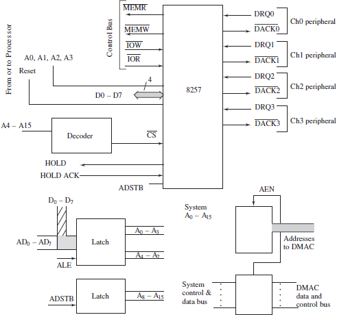
Figure 7.13 Interfacing the 8257 Chip with External Peripherals and Processor Address and Data Buses; A0-A3 Connecting to A0-A3 and CS (Chip-select) Connection to A4-A7 through a Decoder
7.4 PROGRAMMABLE INTERRUPT CONTROLLER 8259
The interrupt-handling mechanism and interrupts handling in 8051 are described in Section 3.7. Interrupt-handling structures in MCUs are described in detail in Chapter 5. Most MCUs may support just two external pins as interrupts. The 8051 supports two external interrupts—INT0 and INT1. Several systems need to connect externally to more than two interrupting sources and devices. For example, a PC connects to two COM port devices (like modem and mouse), printer and CRT interfaces, time of the day signal, CD disk drive and hard disk drive. There is a need for one external interrupt input pin for each device. When there is need for more than one or two hardware interrupts from the external sources, additional circuitory is required. Programmable interrupt controller (PIC) Intel chip 8259 provides the needed circuitory. It is now an industry standard chip. It finds extensive application as an interrupt handler.
Intel 8259 is a classic interrupt controller. It is programmable for masking the interrupts, priority resolution and vectors for the interrupts. [Vector means the address from where the processor finds new service routine (or new service routine address) in case an interrupt occurs.] The 8259 has the following capabilities:
- Eight interrupt request pins. There are 8-levels of priority for the interrupts. These are expandable by cascading up to 64 levels. 8-level means interrupts can be assigned priority 0, 1, …, 7. The 64 level means 0, 1, 2026;, 63.
- Each interrupt request is separately maskable.
- Priority resolution when more than one interrupt is pending service.
- TTL level inputs and outputs.
Figure 7.14(a) shows the block diagram of subunits at 8259 chip. The block diagram gives an overview (for a preliminary understanding) of internal hardware. Figure 7.14(b) shows the configuration of pins at 8259 chip.

Figure 7.14 (a) The Block Diagram of Subunits at 8259 and (b) Uses of the Pins at 8259
Table 7.16 gives the meanings and use of subunits shown in block diagram.
Table 7.16 The Meaning and Use of Subunits in 8259
| Subunits | Use |
|---|---|
Data bus buffer |
An internal buffer register with the data bus. It holds the byte from data bus during write and sends the byte to the data bus during read operations of processor. Write operation is done for programming ICWs (initial command words) and OCWs (operational command words) at 8259. Read operation is for the 8259 status read. |
Priority resolver (P register) |
8-bit register to resolve the priority stores the priorities of 8-interrupts at request (IRQ) pins. Priority sets as per OCW. Default is fully nested priority in order IRQ0 (highest) and IRQ7 (lowest). Priority can also be set to auto rotate (higher priority one after servicing becomes the lowest one) and specific rotation (changing priorities by specifying a device of lowest priority and the next to it as highest). |
Interrupt request register (IRR) |
8-bit register to store the requests from the 8 interrupt-request (IRQ) pins. When a request is services, the corresponding to the request the bit in the register resets. |
Interrupt control logic |
Control logic. |
Interrupt mask register (IMR) |
8-bit register to store the interrupt masks for the 8 IRQ pins. OCW1 programs the IMR. |
In service register (IS register bits) |
8-bit register for in service operations. If 7th IS Register bit = 0, means serviced or service not pending and = 1 means IRQ7 to be or being serviced. (Issuing INTR signal and placing the appropriate bytes during the |
Read/write control logic |
A read/write control logic subunit. Signals are as follows: (a) |
Cascade buffer Comparator subunit |
Used when the 8259 is cascaded with other 8259 to increase the IRQs up to maximum 64 levels. CAS0, CAS1 and CAS2 IO pins selects or shows which of the 8259 out of 8 cascaded together is to be used. [0 at CAS2-CAS1-CAS0 means 0th 8259 and 111 means 7th 8259.] SP-EN pin is to enable the cascade buffer. When SP is input and = 0, it means this 8259 is slave. EN is output and = 0 means this 8259 enabled and presently holds the buses. |
a Figure 7.15 shows the interfacing circuit between 8259 chip and 80x86, 8051 or 68HC11 address and data buses. A0 pin connects to A0. ![]() (chip-select) connects to A1-A15 through a decoder. Table 7.18 gives the addresses for the 8259 when 20H and 21H are the addresses chosen by the processor for writing or reading. Decoding is such that when the processor addresses the 8259 chip for read or write, then only
(chip-select) connects to A1-A15 through a decoder. Table 7.18 gives the addresses for the 8259 when 20H and 21H are the addresses chosen by the processor for writing or reading. Decoding is such that when the processor addresses the 8259 chip for read or write, then only ![]() = 0, else it is 1 for other peripherals or memory addresses.
= 0, else it is 1 for other peripherals or memory addresses.
Table 7.17 gives the meanings and uses of each pin.
Table 7.17 Pins in 8259

a External device negative edge of at least 100 μs duration followed by positive edge transition to 1 requests an interrupt in 8086 mode, at the second cycle of INTA the 8259 places on D0-D7 the 8-bit interrupt level (type). The level enables 8086 to compute 16 bit vector address. In 8085 mode during the first ![]() cycle, the D0-D7 carries call instruction code and in the second and third cycles the LSB and MSB of interrupt vectors address for the service.
cycle, the D0-D7 carries call instruction code and in the second and third cycles the LSB and MSB of interrupt vectors address for the service.
Table 7.18 Addresses for the Programmable Interrupt Controller (PIC) 8259
| Direct Address | Use |
|---|---|
0x20 |
Initial Command Word ICW1. Sequences of codes for the type (level) for the IRQ0 to IRQ7 are written. |
0x21 |
Initial Command Words 2 (For cascade or normal mode), 3 (for automatic or manual end of interrupt) and 4 (for fully nested, automatic or specific rotation mode). |
7.4.1 Interfacing 8259 to Processors
Figure 7.15 shows the interfacing of the 8259 chip with processors (such as 80x86, 8051 or 68HC11) address and data buses, A0 connecting to A0 and ![]() (chip select) connecting to A1-A15 through a decoder.
(chip select) connecting to A1-A15 through a decoder.
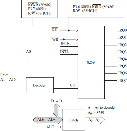
Figure 7.15 Interfacing 8259 Chip with 80x86, 8051 or 68HC11 Address and Data Buses; A0 (Control/data) Connecting to A0 and CS (Chip-select) Connecting to A1-A7 through Decoder
- When AD0-AD7 are the signals, using ALE at the processor, the address A0-A7 bits are latched and then decoded by a decoding circuit.
- The D0-D7 connect to 8259 D0-D7 pins.
- and ( and in 80x86) signals connect to 8259 and pins directly.
- Two addresses for the 8259 device are decided. Assume that these addresses are 20H and 21H. Address bus A0 is directly connected to chip. Upper 7 or 15 bits A1 to A15 are common to both the addresses. Hence, these are used for generating the signal for 8259. Decoder circuit is designed such that when A1 = 1 and A2-A7 = 0s then the decoder output = 0 and connects the ADDR0, ADDR1 and ADDR2 pin.
- The INTR and
 connect INTR and pins at processor.
7.5 ADC CIRCUIT INTERFACING
Analog-to-digital Conversion (ADC)
There are six steps in analog-to-digital conversion:
(1) An ADC (analog digital conversion) circuit is given an analog input; (2) The analog input is given after a sample hold amplifier; (3) The sample hold amplifier samples the signal for a small time interval ts after which it holds the output amplifier and thus analog input Vin remains constant at the ADC for the holding interval th; (4) The ADC is given a start of conversion (![]() ) signal for starting the conversion of Vin to n-bits; (5) ADC converts into digital bits in a time interval tconv. The time interval is called conversoin time; (6) The ADC issues an EOC (end of conversion) signal after the conversion is over. Assume an n-bit ADC. Then the conversion formula is as follows:
) signal for starting the conversion of Vin to n-bits; (5) ADC converts into digital bits in a time interval tconv. The time interval is called conversoin time; (6) The ADC issues an EOC (end of conversion) signal after the conversion is over. Assume an n-bit ADC. Then the conversion formula is as follows:
Vin is analog input voltage. n is the number of ADC bits after conversion. Here (Vref+ − Vref−) is voltage difference between + and − pins for applying reference voltage input.
Example 7.5
Assume (Vref+ − Vref−) = 2.04 V, Vin = 1.032 V. n = 8. Maximum digital value = (28 − 1) = 255. (i) What is the output of an ADC? (ii) What is the resolution of the ADC? (iii) What are the limits for Vin?
- When Vin = 1.032 V, then the output will be 1000 0001 = 129 decimal according to Equation (7.1).
- ADC resolution is 2.040 V/255 = 8 mV. Vin must be less than (Vref+ − Vref−) = 2.04 V and greater or equal to Vref− = 0.000 V.
ADC Conversion Accuracy, Speed and Time
Conversion accuracy is defined by how accurate is the conversion in an ADC with respect to a given reference voltage at ADC. Conversion speed is defined by how fast is the conversion in an ADC. It is measured by number of conversions successfully made per second. Conversion time is defined by after how much time the conversion will be over and end of conversion interrupt generates with respect to a start of conversion signal.
Internal ADC in an MCU
Figure 2.12 showed an internal ADC in an MCU. It showed reference inputs with three possible options in the MCU. Section 2.3.10 described the on-chip ADC features in specific versions of a family. For example, 80535 has an 8-bit ADC and reference voltages Vref+ − Vref− are separately programmable. The 80552 has a 10-bit ADC. It has 8-channel MUX (multiplexer). The MUX enables the use of the same ADC for eight different analog channels.
External ADC Interfaced to an MCU
An external ADC chip interfacing provides the requisite conversion time and other features. These may not be available on the chip in a version of an MCU family or the external ADC may be a cost effective proposition after interfacing it with the low cost ADC-less version. ADC 0804, ADC 0808, and ADC 0816 are the examples of 8-bit ADCs for 1, 8 and 16 channels, respectively. Figures 7.16(a) to (c) show block diagrams of interfacing units for ADC 0804, ADC 0808 and ADC 0816. The block diagrams show the overviews (for preliminary understanding) of hardware. These chips do not have command (control) register. Therefore, these directly interface to port bits of MCU.

Figure 7.16 (a) Interfacing Units and Signals with ADC 0804, (b) Interfacing Units and Signals with ADC 0808 and (c) Interfacing Units and Signals with ADC 0816
Table 7.19 gives the meanings and use of the ADC interfacing in Figure 7.16.
Table 7.19 Meanings and Uses of ADC Interfacing Units
| Subunits | Use |
|---|---|
IC chip voltage reference generator |
A circuit for generating the voltage reference (Vref /2) or Vref+ and Vref−. |
Sample-hold circuit |
To sample the analog input for a period which is set for time interval ts and then hold it till the conversion interval. |
Read/write control logic and channel address latch and out enable circuit |
Circuit enables the ADC to get channel number through the data bus lower four bits when ALE = 1. The circuit inputs are external and are read, write and address-latch enable from the system bus. Circuit enables the ADC to place on data bus the converted bits, when |
Start of conversion, end of conversion (EOC), interrupt and timer-circuit for sampling rate |
There are one output and three inputs (to ADC) through four tristate buffers. EOC generates an interrupt signal to the processor or PIC when interrupt select (INTS) is set (enabled). Timer clock can also generate the periodic interrupts when timer clock by INTS reset is selected. Timer clock signal can also periodically start the conversion or an external start conversion signal (STC) can also start conversion. |
Table 7.20 gives the meanings and uses of each pin for ADC 0816.
Table 7.20 Pins and Their Uses in ADC 0816

Assume that ADC chip selects when addresses are between 0x40 and 0x4F. Table 7.21 gives the addresses of the analog channels. Using an address, the converted bits of a channel are read by a processor read instruction.
Figure 7.17(a) shows the interfacing circuit of the ADC chip with the LSB of lower address and data buses. addr0, addr1, addr2 and addr3 are the addresses of channel sent through AD0-AD3 lines for 16 channels. ![]() (chip-select) connects through a decoder. Decoding circuit is such that when the processor addresses the ADC chip for read or write, then only
(chip-select) connects through a decoder. Decoding circuit is such that when the processor addresses the ADC chip for read or write, then only ![]() = 0, else itis 1 for other peripherals or memory addresses. ADC 0816 conversion time is 110 μs plus there is S/
= 0, else itis 1 for other peripherals or memory addresses. ADC 0816 conversion time is 110 μs plus there is S/ ![]() acquisition time plus S/
acquisition time plus S/ ![]() settling time and IN/OUT instructions execution time. Figure 7.17(b) shows the interfacing circuit of the ADC chip ADC 0808 with the LSB of lower address and data buses. addr0, addr1and addr2 are the addresses of channel sent through AD0-AD2 lines. Figure 7.17(c) shows interfacing the ADC internal device with 68HC11.
settling time and IN/OUT instructions execution time. Figure 7.17(b) shows the interfacing circuit of the ADC chip ADC 0808 with the LSB of lower address and data buses. addr0, addr1and addr2 are the addresses of channel sent through AD0-AD2 lines. Figure 7.17(c) shows interfacing the ADC internal device with 68HC11.
Table 7.21 Addresses for the 16 channel ADC Interface when 40H-4FH are the Addresses Used by the Processor Instructions
| Direct Address | Function |
|---|---|
40H |
Analog Channel 0 Select |
41H |
Analog Channel 1 Select |
4EH |
Analog Channel 14 Select |
4FH |
Analog Channel 15 Select |
Note: Only 40H-47H used for 8 channel ADC0808.

Figure 7.17 (a) Interfacing an External ADC Chip with 8051 Address and Data Buses, (b) Interfacing ADC 0808 Chip with 8051 Ports and (c) Interfacing the Signals to ADC Internal Device in 68HC11
Figure 7.18 shows the programming steps for reading the ADC channels.

Figure 7.18 Programming Steps for Reading the ADC Channels
Considerations when Selecting or Using an ADC
Following are the considerations when selecting or using an ADC:
- Location : Location of ADC should be near the transducer and then converted bits are sent to MCU at a remote location. This arrangement reduces the noise pick-ups during the signal path. It reduces ground loop related error. (Error due to path to ground potential is longer than the active pin signal path.) A transducer is one that gives the form of a value observed for a resistance, capacity or voltage or current or frequency, which is in accordance with the physical value of a parameter. The parameter could be pressure, temperature, light-intensity, linear or angular position. Transducer with appropriate signal conditioner and sample-hold amplifier generates the desired parameter-related analog signal. The signal is the ADC input at an instance. Signal conditioner is a circuit to give outputs for the ADC such that the minimum and maximum values of the parameter being measured give the ADC analog inputs between Vref+ and Vref−. For example, human body temperature can be between 98°F and 105°F. Signal conditioner at the transducer output can generate 0 V for 98°F and 2 V for 105°F.
Example 7.6
Assume that temperature is measured between −40°C minimum to +40°C maximum, and Vref+ = 2.048 V and Vref− = 0.000 V at the ADC. Assume that the transducer is such that it gives 233 μA current when T = −40°C and 313 μA current when T = +40°C. The transducer output should be signal conditioned by an amplifier circuit such that the ADC input is between 0.000 V and 2.048 V when temperatures is between −40°C and +40°C.
- Sampling and data throughput rates: Need for recording more samples per second may be there when recording an analog waveform (for example, an ECG signal). Need of a higher sampling rate may inhibit use of a single ADC for the multiple analog channels. Sample-hold amplifier samples the signal for a specific period to reduce the sharp transitions and noise effects. However, sampling rate is inversely related to sampling time. Sample-hold circuit should use very low-leakage capacitor like polystyrene capacitor.
- Number of analog channels: The number of analog channels may be required in a specific system like data acquisition system.
- CMOS or bipolar-based ADC selection: A CMOS-based ADC advantage is low power dissipation and easy circuitry for multiplexing, latching and decoding. The disadvantage is the low precision of reference voltage and low conversion speed.
- Conversion accuracy: The desired accuracy in conversion is an important criterion. Use of ADC full input range helps in enhancing the accuracy. For example, assume that reference voltage is +2.023 V and input ADC signal is of maximum = +0.5 V. (Assume that negative reference point is at ground level.) We can amplify the input four times before conversion to enhance the conversion accuracy. Consider another example, assume that reference voltage is positive 2.023 V and input ADC signal is of +0.5 V maximum and +0.3 V minimum. (Assume negative reference point is also programmable or can also be fixed) We can amplify the input four times before conversion and fix negative reference at +1.2 V to enhance the conversion accuracy. [Fixing −ve reference other that analog ground is feasible in certain ADC circuits or MCUs.]
- Reference signal: Reference signal precision affects the ADC precision. Hence, reference signal source circuit can be important criteria. Also, choose dual reference (positive and negative) references and programmable references for better accuracy, resolution, and precision (Figure 2.12).
- Separation of analog and digital grounds: Digital ground electrical line carries end noise. The noise arises due to sharp 1 to 0 and 0 to 1 transitions at the logic circuits which cause induced voltages in the neighbouring lines. A decoupling capacitor is placed near the digital circuits for reducing the noise signal. The separation of analog and digital ground lines further reduces the noise and that is the best proposition.
7.6 DAC CIRCUIT INTERFACING
Digital-to-analog Conversion (DAC)
There are three steps in digital conversion from analog:
(1) A DAC (digital-to-analog conversion) circuit is given the digital inputs. For example, 8 bits from 8-port pins. The analog output is obtained after a current amplifier. Vout remains constant at the DAC for the holding interval th, till another pulse for start of conversion (STC) signal is applied to DAC. (2) DAC converts digital bits in a time interval tconv to analog current. The time interval is called conversion time; (3) After the conversion is over, the dAc gives Vout as per conversion formula:
k is a constant dependent on current amplifier at the DAC output. n is the number of DAC bits for conversion. Here (Vref+ − Vref−) is the voltage difference between + and − pins for applying reference voltage input to DAC.
Example 7.7
(Vref+ − Vref−) = 2.04 V. n = 8, Digital input = 1000 0000 = 128 decimal. (i) What is Vout? Assume k = 1. (ii) What is the resolution of DAC?
(i) Using Equation (7.2) the output will be 1.024 V (ii) The DAC resolution is 2.04 V/(28 − 1) = 2.04 V/255 = 8 mV. Resolution multiplied by 128 decimal gives 1.024 V.
DAC Conversion Accuracy and Time
Conversion accuracy is defined by how accurate the conversion is in a DAC with respect to a given reference voltage at DAC. Conversion time is defined by after how much time the conversion will be over and analog output obtained after the change of bits at the DAC input.
Internal PWM in MCU for DAC
On-chip PWM has DAC features. Section 2.3.9 and 2.3.6 explained the PWM feature. Specific versions of a family, for example, 80552 and 80C580 have on-chip PWM. Figure 2.11(b) shows internal PWM (pulse width modulation) feature for the DAC operations using the external integrator with an MCU. The MC68HC11N4 series versions have two channels DAC outputs. Two DAC outputs (at port G bits 5 and 4) are according to the bytes programmed at two data registers of 8-bit each. A control register DCON bits (b0 and b1) are programmed to enable or disable the DA channel 1 and 2, respectively, according to the data registers DA1 and DA2, respectively.
External DAC for Interfacing with MCU
Interface circuit with an external DAC chip provides the requisite conversion time and other features that may not be available on-chip in a version of an MCU family or the external DAC may be a cost-effective proposition after interfacing it with the low cost PWM or DAC-less version MCU. DAC808 and MC1408 are the examples of 8-bit DACs (for 1 channel). Figure 7.19 shows interfacing circuit using DAC 808. These chips have no internal command register. They can also directly interface to port pins of MCU.
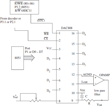
Figure 7.19 Interfacing Units Block Diagram when Using the DAC808 with the 8051
Table 7.22 gives the meaning and use of each pin for DAC 808.
Table 7.22 Pins in DAC 808

Figure 7.20(a) shows interfacing the DAC chip with an MCU or CPU address and data buses, and Figure 7.20(b) shows interfacing the ADC chip with 8051 ports.
Example 7.8
Show the programming steps for generating RAMP-like waveform.
Figure 7.21 shows the programming steps for generating a RAMP waveform output.
Considerations when Selecting or Using a DAC
Following are the considerations when selecting or using an ADC:
- OPAMP amplifier or integrator: An amplifier converts the DAC current output into output voltage of actuator. An actuator is one that gives the output of voltage or current or frequency or power in accordance with physical value of analog input to control a parameter like pressure, temperature, light intensity, linear or angular position. The DAC and appropriate signal conditioner or amplifier generates the desired analog signal for actuator.

Figure 7.20 (a) Interfacing the DAC Chip with any MCU or CPU Address and Data Buses AD0-AD7 and (b) Interfacing the ADC Chip with 8051 Ports

Figure 7.21 Programming Steps for DAC Generating a RAMP Waveform Output
- Conversion rate: This is for changing the analog outputs frequently and generating analog wave-form (for example, a ramp signal for a signal plotter) for higher conversion rate.
- Number of analog output channels: The number of analog output channels may be required in a specific system like an automatic environment control plant or a robot with multiple degrees of freedom with a DC motor for each degree movements.
- Reference signal: Reference signal precision affects the DAC precision. Hence, reference signal source circuit can be an important criterion.
- Separation of analog and digital grounds: Digital ground carries noise. It arises due to the sharp 1 to 0 and 0 to 1 transitions in digital circuits. A decoupling capacitor is placed near the digital chips to reduce noise. The separation of analog and digital grounds is also done.
7.7 INTER-INTEGRATED CIRCUITS INTERFACING (I2C BUS STANDARD)
Interconnection Using a Bus
Advantage of doing interconnection using a bus is simplicity of wiring. Though several devices and systems or units are interconnected but only the destined unit accepts (receives) or sends (transmits) the data and others ignore the bus signals. Consider address and data buses. These are parallel buses as all address signals A0 to A15 are sent in parallel and all D0-D7 signals are parallel [Figure 1.1]. Parallel buses are difficult to use for interconnecting the remote units and devices.
Interconnection Using a Serial Bus
Advantage of doing interconnection using serial bus is that the interconnection of the units is done with one or two or four wires only. Only the destined unit accepts (receives) or sends (transmits) the data, and others ignore the serial signals
Interconnection Using a UART Serial Bus
One possible way, we have learnt for interprocessor serial communication in Section 3.6.3. We learnt how to use theSM2, TB8 and RB8 bits for serial bus communication and 8051 in UART mode This method is for the serial UART communication between interconnected 8051 MCUs only.
Interconnection Using a Synchronous Serial Bus
I2C synchronous serial bus is originally from Philips since 1970. It provides one of the standard methods (protocol). It serially interconnects the integrated circuits (ICs). It is popularly used in the serial communication networks of embedded devices.
It can be used for systems with multiple masters and slaves on the bus. Master means a smart device that can initiate data transfers. Slave means a device that acknowledges and responds to the request of the master device. A device can also work in master mode at one instance and in slave mode in another instance.
Built-in Interface for I2C Bus in 8051 Versions
A version of 8051 family may also have a built-in interface for I2C bus. There are two signals on I2C bus—SDA (serial data) and SCL (serial clock). Philips P83C528 is an 8051 version from Philips with P1.6 pin for SCL and P1.7 pin for SCL.
I2C Bus Signals and Serial Communication Rate
I2C bus operates at 100 kbps, 400 kpbs and 3.4 Mbps (2 m). Figure 7.22(a) shows I2C bus interface. There are two signals SDA (Serial Data) and SCL (Serial Clock) between 8051 and four I2C devices at P1.7 and P1.6, respectively.
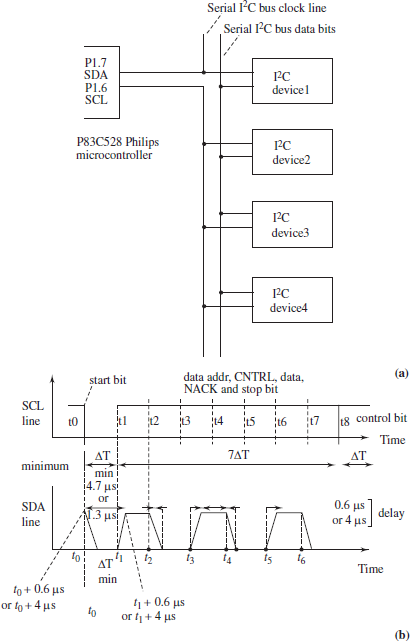
Figure 7.22 (a) I2C Bus Interface with Two Signals SDA (Serial Data) and SCL (Serial Clock) Between the 8051 and Four I2C Devices and (b) Two Signals and the Delay Between the +ve Edges of SCL with Respect to SDA
The signals have internal pull ups. Internal pull up means the transistor at output stage internally connected to 5 V through a resistance to draw (pull) finite currents on logic 0 or 1. External bus current requirement increases when the multiple devices interconnect. Therefore, intervals of 1 μs between clock pulses and of 0.5 μs intervals between SDA and SCL increase. An external R = 1 kOhm to 2.2 kOhm pull up to 5 V with each of these signals can be additionally placed. This ensures that the intervals do not get extended because of loading.
Figure 7.22(b) shows the delay between the positive edges of SCL with respect to SDA.
Logic 1 is for ΔT = 4 μs in standard bus and for 0.6 μs in fast bus. Bit transmits during logic 1. Start bit is at logic 0. Start bit minimum interval ΔT is 1.3 μs in fast bus and 4.7 μs in standard bus. A protocol is used for sending the bits or bytes on a serial line. It gives the sequencing of the bits before and after the data bits.
I2C Bus Protocol
A protocol is followed for sending the bits or bytes on a serial line. It specifies sequencing of the bits before and after the data (message) bits. Assume one bit time interval = ΔT. Figure 7.23 shows the bits sequencing in I2C bus.
Protocol provides for addressing to slaves by a master and sending messages between the master and slave. (Addressed slave sends the response when master sends (places) the request for that on the bus). The following are the fields in bit sequences on I2C bus:
- The master sends the output at SDA line for 8×ΔT for the first and second fields. First field is the start bit. Second field has next seven bits. These are bits for slave address. The maximum significance bit (msb) is sent first and least significance bit (lsb) at the last. Usually, four msbs can be used to specify the device type and the next three lsbs to select one of the 8 devices of that type. For example, 0010 specifies RF tuning control, 0100 audio tone generating device, 0011 PCM audio-interface and 1000 video-interface as the device type.
- Third field has 1 control bit for ΔT. It specifies whether write or read cycle is in progress. The slave can put the acknowledgement bit after that during the fourth field. Master goes in input mode for SDA for that ACK bit time interval of AT. Fourth field thus specifies whether the present data is acknowledgement from slave.
- Fifth field is of 8-bit data (or command) from master. Sixth field is 1 bit NACK (negative acknowledgement). If active, then it means acknowledgement not needed from the slave if transfer successful, else acknowledgement is expected from the slave.
- The last (seventh) field is stop bit like in an UART.

Figure 7.23 I2C Bus Protocol First to Seventh Fields
Figure 7.24 shows the example of steps in programming of serial transfer from master and first and second fields in 8051 built-in I2C bus interface. Assume that there is only one master.

Figure 7.24 Example of Programming Steps when Using 8051 Built-in I2C Bus Interface
I2C bus is relatively slow. CAN (Controller Area Network) bus, USB (Universal Serial Bus) and IEEE 1394b are three other popular serial buses.
SUMMARY
- External UART 8250 or USART 8251 are programmable serial communication devices. It can be interfaced to the DCE like a modem. It can be programmed for 1 or 2 or 1½ stop bit.
- There are three modes of data transfer between the system memory and external peripherals: (a) busy and wait programmed IO, (b) interrupt- driven and (c) DMA controlled transfer.
- External PPI 8255 is a programmable parallel ports device.
- Ports can be programmed in the without handshake, handshake, bi-directional handshake modes.
- DMAC 8257 is a four-channel DMAC that provides direct memory access channel to a device once it is programmed for DMA address (start address of the memory block) and terminal counts for that channel for that channel.
- PIC 8259 is an interrupt controller for the eight interrupt request signals from the external devices. It can mask a request and has programmable priority resolver.
- ADC 0804, 0808 and 0816 are the one, eight and sixteen channel ADCs. Each converts analog input into 8 bits. Analog input is from the sample hold amplifier. The voltage reference source, read-write logic and start and end of conversion circuits are required for the operations. Signals from transducer connect a signal conditioning circuit when measuring a physical parameter like temperature. The signal conditioner adjusts the range of analog input to the ADC.
- DAC 808 is an 8-bit DAC. It has no internal command register and can thus directly interface the port bits also.
- I2C is a synchronous serial bus that can be used to interconnect several masters and slaves in a microcontroller or ICs network.
- CAN, USB and IEEE1394 are other device network interface protocols.
KEY TERMS
Actuator: A circuit that generates voltage or current or power or frequency in a system that controls physical conditions like temperature, pressure and sound. A loudspeaker is an example of actuator.
ADC: Analog-to-digital conversion after comparison with a reference voltage. When analog input equals one at +ve reference pin, the outputs are all 1s and when equal to one at the −ve reference pin, the outputs are all 0s.
CAN: Controller area network is a serial bus standard popular particularly devices and controllers networks in the automobile system.
Command instruction: A control byte or word written by a processor instruction into a programmable device to program the actions at the device, for example, enables the device by setting a bit or by resetting a bit. Control word(s): A byte or word written by a processor instruction into a programmable device to program the device modes and to command the device.
Conversion accuracy: With respect to a given reference voltage how accurate is the conversion in an ADC or DAC.
Conversion speed: How fast is the conversion in an ADC or DAC, it is measured by number of conversions successfully made per second.
Conversion time: With respect to a start of conversion signal, after how much time the conversion will be over and end of conversion interrupt generates.
DAC: Digital-to-analog converter after comparison with a reference voltage. The analog output equals reference when the input bits are all 1s and equals −ve reference when the bits are all 0s.
DACK: A signal generated as acknowledgement by the DMAC after a peripheral requests the DMA transfer. Data bus buffer: A buffer to hold a byte before it is read by the processor instruction or after it is written by the processor instruction.
DCE: Data communication equipment that uses a line or channel such as a mobile or wired or wireless link for communicating with the serial data. It interconnects the DTE. DCE example is a modem.
DMA address register: A register where the address of the memory is loaded to enable DMAC to read or write there by direct transfer, which takes place using the system buses when accessible.
DMA controller: A device to facilitate direct transfer of bytes between the system memory and external peripherals such as CD disk controller and hard disk controller and transfers the needed bulk data without frequent processor interrupt.
DRQ: A signal generated by peripheral for DMAC to request the DMA transfers and the DMAC sends back the DACK to enable the peripheral to start the transfer.
DTE: Data terminal equipment that uses a port like COM port (RS232C port) to link a line or channel like a telephone link using the DCE between. Example of DTE is an IBM PC.
Handshaking signals: Signals between a device and another device and one is for request and other is for acknowledgement of that request. Using handshaking signals and a control signal (interrupt), the device is able to transfer the bytes an in interrupt-driven mode or vice versa.
I2C bus: A synchronous serial bus for inter-integrated circuits communication.
In-service register: A register in 8259 to hold the bytes for a specific request being serviced by PIC.
Interrupt control signal: An interrupt to CPU after an output transfer is complete or after a input becomes available.
Interrupt mask register: A register in 8259 to hold the bits that are set for the requests that are masked and reset for those which are unmasked. For example, when bit 0 = 0, IRQ0 request is unmasked and when bit 4 = 1, IRQ4 request is masked.
Interrupt request register: A register in 8259 to hold the bits that are set for the requests that are pending and needing service and reset for those which are either serviced or not pending. For example, when bit 0 = 0, IRQ0 request is not pending and when bit 4 = 1, IRQ4 request is pending.
Keypad: A set of about 16 keys, for example, in a mobile phone or telephone or calculator to give input to the systems using a port(s) directly or through a keypad controller.
Mode instruction: A control byte or word written by a processor instruction into a programmable device to program the device mode by setting a bit(s) or by resetting a bit(s).
Modem control: The signals DSR (data set ready from DCE), DTR (data terminal ready from DTE), RTS (request to send from DTE), CTS (clear to send from DCE), RI (ring indicator), DCD (data carrier detect) are the modem control (by handshaking) signals between the DCE and DTE.
Parallel port: A port that can connect using data bus line to the processor and using IO pins to the external device (peripheral).
PIC: Programmable interrupt controller 8259 chip from Intel.
PPI: Programmable peripheral interface 8255 chip from Intel.
Priority resolver: A unit to resolve the priority before the service in a PIC or DMAC when there are several sources of interrupt or devices. Priority can be resolved in nested mode or rotation mode or specific rotation mode as per the control bits (operation command bits).
Protocol: A standard program or standard method by which the serial or parallel bits are sequenced on the line in a network.
PTS (peripheral transaction server): A DMAC called as PTS in 80960 and 80196 MCUs.
Reference signal: A signal acting a reference in an ADC or DAC. It is compared with the analog signal and ratio of that is as per the digital bits generated at outputs of ADC or inputs of DAC.
Sensor: An element or circuit used to modify the current or voltage or state of circuit according to the physical parameter such as light or pressure or magnetic field.
Signal conditioner: An amplifier, scalar, adder or integrator circuit so that the range of the outputs is between the maximum and minimum in order to get maximum conversion accuracy. For example, human body temperature can be between 98°F and 105°F. Signal conditioner can generate 0 V for 98°F and 2V for 105°F.
Status word: A word (byte or bytes) in a programmable device that is read by a processor instruction to get the current status of the device.
Stepper motor: A motor with four inputs and left or right shifting the bits rotate the motor by one step. For example, input 0001 changed to 0010 by shifting will rotate the motor by one step.
Stop bit: A mark bit (=1) for minimum one unit interval after a byte is communicated by an UART. Two stop bits mean two unit intervals and it is minimum time before the next byte can be started.
Synchronization character(s): Character(s) preceding the data bits. This enables synchronization of the receiver clock and also enables the use ofjust one serial line in place of two (SDA and SCLK).
Terminal count register: A register where the number of bytes are loaded to enable DMAC to read or write there by direct transfer, which takes place using the system buses when accessible. It decrements on each transfer. When it becomes 0 on continuous decrements, an interrupt or TC signal becomes active to enable the processor to intervene. Every decrease of TC by 128 can also generate a Mark signal, for example, in 8257.
Transducer: A unit to generate a transfer signal to enable the acquisition system to find the physical value of the parameter, like sound level, temperature. A microphone is an example of a transducer.
USB: Universal serial bus standard that enables us to connect the scanner, joystick and other devices serially. Devices can network in a tree-like structure also when using USB.
REVIEW QUESTIONS
- If an MCU has asynchronous and synchronous communication interface, when do you need the additional 8251 USART chip?
- List the programmable features of 8251.
- List the various units within the 8251.
- Describe the use of modem-control and read-write logic pins at 8251.
- When do you need the additional 8255 PPI chip when an MCU has ports?
- List the programmable features of 8255.
- List the various units of 8255.
- Describe the uses of 8255 read-write logic and Port C pins.
- Explain with an example each of the following: busy and wait programmed IO, interrupt-driven and DMA controlled transfer modes.
- When will you prefer DMAC 8257 and when do you prefer interrupt-driven transfers using 8255? [Hint: Consider the number of bytes that need to be transferred.]
- How will you program Port A as a bi-directional port with handshake and interrupt control signals?
- How will you program Port A and B for the programmed I/O transfer?
- How will you interface the 8051 with the ADC 0816 using Port P0 and P2 for address and data buses?
- List the programmable features of 8257.
- List the various units within the 8257.
- Describe the use of the 8257 read-write logic and control logic. Explain the mode set register subunit. Write the use of each 8257 pin. What is the possible application of mark pin to signal every 128th transfer?
- Explain the uses mode set register bits of DMAC 8257.
- How will you interface the 8051 and 8257 with two IO peripherals? Illustrate with a circuit diagram.
- If an MCU has built-in interrupt-handling mechanism, when do we need the additional 8259 PIC?
- List the programmable features of 8259.
- List the various units within the 8259.
- Describe the uses of 8259 internal registers.
- Explain the use of cascading pins of 8259.
- What are the merits and demerits of CMOS- based ADCs?
- How do you interface ADC 0804 with the port pins of 8051?
- What are the advantages of the (i) ADC with dual polarity analog inputs, and (ii) feasibility and internal programmability of both +ve and −ve reference voltages?
- Describe DAC 808 circuit and its operation when interfaced to 8051.
- How does the serial line differ from serial bus?
- Describe all the bits during the serial transfer from the master in an I2C interface device.
- List the advanced serial buses.
PRACTICE EXERCISES
- How will you reprogram 8251 as 7-bit data, even parity and 1½ stop bit UART mode transmission with baud rate (one-sixteenth) of clock rate? (Assume address of data buffer 0060H and of control words 61H.)
- How will you program the 8251 for 7-bit data, odd parity and two sync character byte as 11010010 and 00101101 USRT mode with bit-clock rate?
- Make a table as follows. Command instruction bits that you will program in different modes of serial communication.

- How will you interconnect the 8251 with a modem?
- How will you interconnect the 8251 at the addresses F000H and F001H?
- There are 8 motors (0th to 7th) in a robot for each degree of freedom. How will you interface these to switch the 3rd motor using the 8051 and 8255 direct bit set-reset mode?
- There are 8 LEDs (0th to 7th) in a row. How will you interface these to show the time in minutes for which the washing is ON in a washing machine? Assume that time (in unit of a minute) stores at in a memory location 2000H. Use the 8051 and 8255 direct bit set-reset mode to switch 0 th LED flashing during the first minute, after the first minute, the LED is permanently ON and the 1st LED flashing, after the second minute the 0th and 1st LED are permanently ON and 2nd LED flashing.
- How will you program the DMA address register and Terminal Count register of Ch0 and Ch1?
- How will you mask the IRQ3 and IRQ4 in 8259?
- Assume use of nested priority resolution in 8259. How will you allocate the IRQ pins for: Keypad, printer and timer interrupts?

- Draw the interfacing circuit of 8257 with 8051 address and data buses. Assume Ch0 register starts from F020H.
- How will you interface the 8051 with 8255 port bits connected to the ADC 0816?
- Search the Web for an 8051 version having internal ADC with both +ve and -ve reference voltages internal programmability.
- Search the Web and make a table for finding the following:
- Search the Web and find five versions of MCUs with I2C bus interface pins.
- Show the timing diagram for SDA and SCLK signals in I2C bus interface. Show the time slot in which the receiver acknowledgement is expected.
MULTIPLE CHOICE QUESTIONS
- Which of the options is/are correct?
- 8251 can interface with the RS232C TxD and RxD while 8051 SI cannot
- Both can interface with the RS232C TxD and RxD
- 8051 provides both synchronous and asynchronous communication
- 8251 provides both synchronous and asynchronous communication with a modem or DCE control signals.
- A 8251 mode instruction, two sync characters and command instruction programming will require
- four addresses
- two addresses
- eight addresses
- one address only
- In 8251
- TxEmpty signal is at the external pin
- TxEmpty is a flag, which sets in the status register
- TxEmpty is a flag, which resets in the status register on transmitter buffer empty
- TxEmpty signal is at the external pin as well as sets a flag in the status register on Tx buffer empty.
- 8255 Port’s A bit 7 is to be toggled (if 1 to be made 0 and if 0 then 1). Which of the following processor write instruction will do that?
- Send accumulator byte to Port A after XOR operation with 1000 0000
- Send accumulator byte to Port A after XOR operation with 0111 1111
- Send accumulator byte to Port A after subtracting with 1000 0000
- Use bit set-reset mode of 8255
- 8255 Modes 0, 1 and 2 and bit set-reset mode are programmed by bits
- b7, b6 and b5
- b7, b6, b5 and b2
- b7
- b0-b7
- 8255 control word bit 0 = 0 means
- Port C lower four bits as input in Mode 0 Group B
- PC0 as output
- Port C lowest bit as output in Mode 1 Group B
- Port C lower four bits as output in Mode 0 Group B
- 8257 is for DMA transfer
- from peripheral to RAM
- from RAM to peripheral
- between peripheral and RAM
- between floppy disk controller and RAM
- 8257 DMAC can transfer
- with Ch0 highest priority
- with Ch0 highest priority as well as rotating priority
- with Ch3 highest priority
- with Ch3 highest priority as well as rotating priority
- 8059 PIC
- provides the interrupt type on D0-D7 in 80x86 mode of operation
- provides the interrupt vector LSB address on D0-D7 in 80x86 mode of operation
- provides the interrupt type on A0-A7 in 80x86 mode of operation
- provides the interrupt vector LSB address on A0-A7 in 80x86 mode of operation
- 8259 mask register byte is written as 01010000. Then
- IRQ6 and IRQ4 are unmasked
- IRQ6 and IRQ4 are masked
- IRQ is unmasked and cannot be masked again
- IRQ6 and IRQ4 are masked and cannot be unmasked again
- An ADC 0804 is measuring analog inputs up to 500 mV. Which one will you prefer?
- Use 1.023 V as (reference volatge/2) input and amplifier with a gain of 2
- Use 1.023 V as (reference volatge/2 ) input and amplifier with a gain of 4
- Use 1.023 V as (reference volatge) input and amplifier with a gain of 1
- Use 5 V as (reference volatge ) input and amplifier with a gain of 4
- A DAC output uses a low pass filter
- for line noise filtering
- to reduce the effect of sharp 1 to 0 transition and 0 to 1 transitions at the DAC input
- to drive low frequency output
- to drive dc motor
- Serial line for interprocess communication and serial bus differs in the following:
- serial bus can address several processors and type of devices with bus interface and inter connects multiple masters and slaves
- serial line cannot address the several processors
- serial line can connect up to 16 processors only
- serial bus can address several processors and type of devices with bus interface and inter connects a master with the multiple slaves
- DMAC uses the bus access
- till the end of the TC is reached after which, it sends the hold signal to the processor
- uses the IO bus access only
- till the end of the TC is reached after which, it sends the processor the hold acknowledge signal
- during the intervals in which the bus access is provided at the regular intervals by the processor and when the latter does not need the buses
FILL IN THE BLANKS TYPE QUESTIONS
- 1. 8251 _____ on power up reset.
- 8251 _____ is a chip and is used for _____.
- 8255 has _____ addresses, which are used for Port _____, _____, _____ and control word.
- 8255 facilitates _____ set or reset of individual _____ at Port _____.
- Number of handshaking signals when using 8225 Port as bi-directional buffer = _____ and their names are _____.
- 8255 has total _____ port pins and _____ groups of ports.
- Decoding circuit is used for _____ before a peripheral chip.
- 8237 is used for _____.
- Direct memory access advantage is _____ and it is used when _____.
- 8259 is used for _____.
- Functions of priority resolver in 8259 is _____.
- Functions of in-service register in 8259 is _____.
- Transducer is used for _____ and interfaces to ADC through _____ circuits.
- Actuator is used for _____ and interfaces to DAC through _____ circuits.
- Assume (Vref+ − Vref−) = 2.048 V, Vin = 1.2024 V. n = 8. The output of an ADC _____ _____ when Vin = 0.512 V.
- (Vref+ − Vref−) = _____ when Vin = 1.024 V and n = 8 and output of an ADC = 10000000.
- Vin = 0.024 V then output = 00000011. Resolution of the ADC is _____.
- Vref+ − Vref− = V. n = 8, Digital input = 1000 0000 = 128 decimal. Vout =1.024 V.
- The resolution of DAC is _____ when DAC input 00000010 gives analog output = 0.016 V?
- I2C bus is used for _____. The time interval between SDA bits = _____.