
Chapter 2
Register-Transfer Level Design
Logic synthesis works on register-transfer level (RTL) designs. What logic synthesis offers is an automated route from an RTL design to a gate-level design.
For this reason, it is important that the user of logic synthesis is familiar with RTL design to the extent that it is second nature. This chapter has been included because many designers have never used RTL design formally. This chapter serves as a simple introduction to RTL design for those readers not familiar with it. It is not meant to be a comprehensive study but it does touch on all the main issues that a designer encounters when using the method.
RTL is a medium-level design methodology that can be used for any digital system. Its use is not restricted to logic synthesis: it is equally useful for hand-crafted designs. It is an essential part of the top-down digital design process.
Register-transfer level design is a grand name for a simple concept. In RTL design, a circuit is described as a set of registers and a set of transfer functions describing the flow of data between the registers. The registers are implemented directly as flip-flops, whilst the transfer functions are implemented as blocks of combinational logic.
This division of the design into registers and transfer functions is an important part of the design process and is the main objective of the hardware designer using synthesis. The synthesis style of VHDL has a direct one-to-one relationship with the registers and transfer functions in the design.
RTL is inherently a synchronous design methodology, and this is apparent in the design of all synthesis tools.
This chapter outlines the basic steps in the RTL methodology. It is recommended that these basic steps are used when designing for logic synthesis. To illustrate the connection between RTL and logic synthesis, the examples will be written in VHDL. You are not expected to understand the full details of the VHDL at this stage, but all the VHDL used will be covered in later chapters.
The basis of RTL design is that circuits can be thought of as a set of registers and a set of transfer functions defining the datapaths between registers. The method gives a clear way of thinking about these datapaths and trying different circuit architectures while still at an abstract level.
The first stage of the design is to specify at a system level (i.e. not RTL) what is to be achieved by the circuit. Typically this will be a set of arithmetic and logic operations on data coming in at the primary inputs of the circuit. At this stage there is no hardware implementation in mind; the purpose is just to create a simulation model that can then be used as the formal specification of the design. At this stage the system-level model looks more like software than hardware. The system-level model can also be used to confirm with a customer that their design requirements have been understood. Even at this early stage in the design, long before the RTL design process is complete, it is possible to write a VHDL model for simulation purposes only (not intended to be synthesisable). This is a worthwhile exercise since it tests the understanding of the problem and allows the algorithm to be checked for correctness. Later, this VHDL model can be used for comparison with the completed RTL design to verify the correctness of the design procedure. This ability to cross-check different representations of a design in the same design language using the same simulator is a powerful feature of VHDL.
The second stage of the design is to transform the system level design into an RTL design. It is rare for a design to be directly implemented in exactly the same form as the system-level model. For example, if the design performs a number of multiplications or divisions, the circuit area of the direct implementation would be excessive.
The basic design steps in using RTL are:
- identify the data operations;
- determine the type and precision of the operations;
- decide what data processing resources to provide;
- allocate operations to resources;
- allocate registers for intermediate results;
- design the controller;
- design the reset mechanism.
The VHDL model of the RTL design can be simulated and checked against the system design.
The third stage of the design is to synthesise the RTL design. The resulting gate-level netlist or schematic can be (and should be) simulated against the RTL design to confirm that the synthesised circuit has the same behaviour.
Finally, the netlist or schematic produced by synthesis is supplied to the placement and routing tools for circuit layout.
Needless to say, the design will probably need to go through the design/synthesise/layout cycle several times with minor or even major modifications before all the design constraints are met. Synthesis does not eliminate the need to re-iterate designs, but it does speed up the iteration time considerably.
The best way to illustrate the RTL design method is with an example. In this case, the example will be a quite artificial circuit for calculating the dot product of two vectors.
The dot product of two vectors is defined by:
![]()
For the purpose of this example, to keep it simple, the size of the vectors will be fixed at 8 elements.
The system-level model in VHDL is:
package dot_product_types is
type int_vector is array (0 to 7) of integer;
end;
use work.dot_product_types.all;
entity dot_product is
port (a, b : in int_vector; z : out integer);
end;
architecture system of dot_product is
begin
process (a, b)
variable accumulator : integer;
begin
accumulator := 0;
for i in 0 to 7 loop
accumulator := accumulator + a(i)*b(i);
end loop;
z <= accumulator;
end process;
end;
This VHDL model is generally referred to as the system model. It is the simplest possible statement of the algorithm to be carried out, with no regard for data precision, timing or data storage.
In fact, since this is a very simple example, it is possible to synthesise this system model. This would not normally be the case and it should be assumed during the system modelling phase that the full range of VHDL can be used since the result is never going to be synthesised. In this example, synthesising the system model is of interest because it will give a means of comparison so that the effect of the RTL design process can be measured.
The system model was synthesised using a commercial synthesis system and targeted at a commercial ASIC library. It is not relevant which system and which library because the purpose of performing the synthesis is just to compare this direct implementation of the algorithm with the RTL model that will be developed over the rest of the chapter.
The results of synthesis were
- area – 40 000 NAND gate equivalents;
- I/O – 546 ports;
- storage – 0 registers.
It can be seen from the lack of registers that the system model synthesises to a purely combinational circuit. This circuit contains eight multipliers and seven adders. One of the reasons why this is such a large circuit is that the standard interpretation of integers is a 32-bit 2's complement representation. This means that the multipliers and adders are all 32-bit circuits.
Clearly the direct implementation of the system model is unacceptable and a better solution should be sought. This is where RTL design comes in.
2.3 Identify the Data Operations
The first stage in the design process is to identify what data operations are being performed in the problem. This can be seen more clearly in the form of a data-flow diagram showing the relationship between the datapaths and the operations performed on them. This is illustrated in Figure 2.1.
Figure 2.1 Cross-product calculator – data-flow diagram.
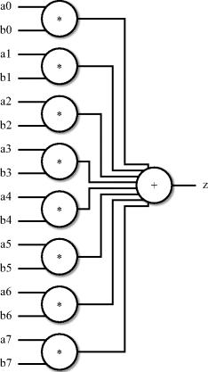
It can be seen from this diagram that the dot-product calculation requires eight 2-way multiplications and one 8-way addition. These are the basic data operations required to perform the calculation.
At this stage the type of the operation should also be considered. Are the calculations acting on integers, fixed-point or floating-point types? Will a transformation be needed? For example, performing floating-point calculations is very expensive in hardware and time, so significant speed and area improvements could be made by recasting the problem onto fixed-point or even integer types.
For this example, all the operations are assumed to be 2's-complement integer arithmetic.
The diagram also shows the dependencies on the data operations. The multiplications can be performed in any order or even all simultaneously since they are independent of each other. However, the additions must be carried out after the multiplications.
The additions have been lumped together as one operation. In practice, the additions will be performed as a series of two-way additions. They are lumped together in the figure because the ordering of the additions is irrelevant and can be chosen by the designer at a later stage in the design process so as to simplify the circuit design. This means that there are a number of structures for the data-flow diagram depending on the chosen ordering of the additions. The optimum ordering of these two-way additions will often become obvious as a design progresses. The two most likely candidates for the ordering of the additions are shown in Figures 2.2 and 2.3.
Figure 2.2 Adder – balanced tree.
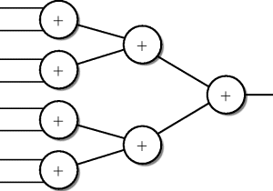
Figure 2.3 Adder – skewed tree.
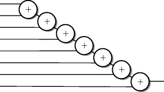
The different orderings of adders place different requirements on the ordering of the multiplications. The balanced tree for example allows an addition to be performed when any two adjacent multiplications have been performed. The multiplication pairs can be performed in any order or simultaneously. The skewed tree on the other hand places a stricter ordering on the multiplications but allows an addition after every multiplication except the first.
No decision will be made at this stage of the design process, but it will become clear later in the design process that the skewed tree data-flow turns out to be the ordering for the chosen solution for this design.
Note that the two orderings of the additions illustrated here, and indeed all of the possible orderings, require seven 2-way additions.
In conclusion then, the data operations required to perform the dot-product calculation are:
- 8 multiplications;
- 7 additions.
2.4 Determine the Data Precision
In a real design, the specification would place requirements on the design, such as the expected data range, the required overflow behaviour and the maximum allowable cumulative error (for example when sampling real-world data). These factors will vary from design to design, but the key step in the design process will always be the same: to assign a precision to every data-flow such that the design meets the requirements.
This example is for illustration only, so the precision of the calculations will be chosen arbitrarily. In this case overflow during the addition will be allowed but will be ignored to keep the example simple.
In this example the following will be assumed:
- data inputs 8-bit 2's-complement;
- all other datapaths 16-bit 2's-complement.
2.5 Choose Resources to Provide
Having determined the data operations to be performed and the precision of those operations, it is now possible to decide what hardware resources will be provided in the circuit design to implement the algorithm.
In the simplest case, there would be a one-to-one mapping of operations onto resources. This would be a direct implementation of the algorithm in hardware. In this example, a direct implementation would require eight 8-bit multipliers (with 16-bit outputs) plus seven 16-bit adders. This is the same circuit as the system specification but with reduced precision on the datapaths.
Since this is just an example, there are no design constraints as such. However, for the purposes of the exercise, it will be assumed that there are design constraints that effectively restrict the hardware resources to one multiplier. The system will be clocked and the result accumulated over several clock cycles. No limit is placed on the number of clock cycles that can be used or on the length of the clock cycle, but it will also be assumed that a complete multiply and add can be performed in one clock cycle. This means that, since there is only one multiplier, the design also only needs one adder.
So, in summary, the hardware resources available are:
- one, 8-bit input, 16-bit output, multiplier;
- one, 16-bit input, 16-bit output, adder.
2.6 Allocate Operations to Resources
The next stage in the RTL design cycle is commonly referred to as Allocation and Scheduling. Allocation refers to the mapping of data operations onto hardware resources. Scheduling refers to the choice of clock cycle on which an operation will be performed in a multi-cycle operation. Registers must also be allocated to all values that cross over from one clock cycle to a later one. Allocation and Scheduling are interlinked and normally must be carried out simultaneously. The aim is to maximise the resource usage and simultaneously to minimise the registers required to store intermediate results.
Due to the simplicity of this example, the allocation stage is trivial since all multiplications must be allocated to the one multiplier and all the additions to the one adder.
The scheduling operation means choosing which clock cycle each multiplication and addition is to be performed. This is confused slightly by the fact that all the additions are interchangeable. Since the specification allows a multiplication and an addition in one clock cycle, the schedule can allow the product of a multiplication to be fed directly to the adder in the same clock cycle, therefore avoiding an intermediate register.
The scheduling and allocation scheme is illustrated by Table 2.1.
Table 2.1 Scheduling and allocation for cross-product calculator.
| Cycle | ∗ Operator | + Operator |
| 1 | a0∗b0 ⇒ product0 | 0 + product0 ⇒ result |
| 2 | a1∗b1 ⇒ product1 | result + product1 ⇒ result |
| 3 | a2∗b2 ⇒ product2 | result + product2 ⇒ result |
| 4 | a3∗b3 ⇒ product3 | result + product3 ⇒ result |
| 5 | a4∗b4 ⇒ product4 | result + product4 ⇒ result |
| 6 | a5∗b5 ⇒ product5 | result + product5 ⇒ result |
| 7 | a6∗b6 ⇒ product6 | result + product6 ⇒ result |
| 8 | a7∗b7 ⇒ product7 | result + product7 ⇒ result |
The whole operation of calculating the dot-product takes eight clock cycles. The algorithm has been simplified slightly by adding an eighth addition in the first cycle that effectively resets the accumulated result by adding 0 to product0 instead of adding the result so far. This saves the need for a reset cycle.
Only one register is required by this scheduling since the only value that needs to be saved from one clock cycle to another is the result that is accumulated over the eight clock cycles.
It is now possible to design the datapath part of the circuit minus its controller. The datapath consists of a multiplier with two inputs, one multiplexed from the set of a0 to a7, the other multiplexed from the set of b0 to b7. The product is then added to either the accumulated result or 0. Finally, the accumulated result is saved in a register. The circuit is shown in Figure 2.4.
Figure 2.4 Cross-product calculator – datapath.
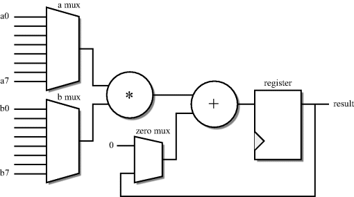
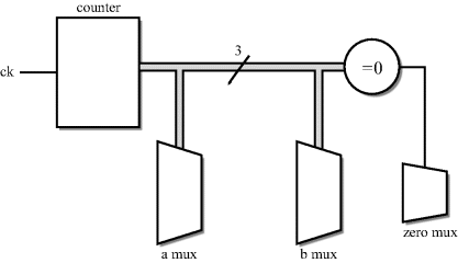
The penultimate stage in the design of the dot-product calculator is to design a controller to sequence the operations over the eight clock cycles. There are three multiplexers and a register to control in this circuit. Their operation for each of the eight clock cycles is shown in Table 2.2.
Table 2.2 Controller operations per clock cycle.

It can be seen that the multiplexers selecting between the a and b vector elements have identical operation; the zero multiplexer selects the zero input on clock 1 and the result input all the rest of the time; the register is permanently in load mode and so needs no control.
Normally, the controller would be implemented as a state machine. However, in this case, the state machine can be simplified to a counter that counts from 0 to 7 repeatedly. The output of the counter controls the a and b multiplexers directly. A zero detector on the counter output controls the zero multiplexer. The circuit for the controller is illustrated by Figure 2.5.
Figure 2.5 Cross-product calculator – controller.
2.8 Design the Reset Mechanism
The final stage of the RTL design is to design the reset mechanism. This is a simple, but essential stage of the design process. The design of a reset mechanism is an essential part of the design of the RTL system, although it is often the case that only the controller needs a reset control. If the reset mechanism is not designed into the RTL model, then there is no guarantee that the circuit will start up in a known state.
In this case, it is sufficient to reset the controller. The datapath will be cleared by the design of the controller, which resets the accumulator anyway at the start of the calculation. The controller's reset will be incorporated as a synchronous reset.
2.9 VHDL Description of the RTL Design
Now that the RTL design process has been completed, a VHDL model can be written. This model can be simulated to verify correct behaviour by comparison with the system model that we started with. The difference is that the RTL model is clocked and needs eight clock cycles to form a result, whilst the system model was combinational and formed the result instantaneously.
library ieee;
use ieee.std_logic_1164.all, ieee.numeric_std.all;
package dot_product_types is
subtype sig8 is signed (7 downto 0);
type sig8_vector is array (natural range <>) of sig8;
end;
library ieee;
use ieee.std_logic_1164.all, ieee.numeric_std.all;
use work.dot_product_types.all;
entity dot_product is
port (a, b : in sig8_vector(7 downto 0);
ck, reset: in std_logic;
result : out signed(15 downto 0));
end;
architecture behaviour of dot_product is
signal i : unsigned(2 downto 0);
signal ai, bi : signed (7 downto 0);
signal product, add_in, sum, accumulator : signed(15 downto 0);
begin
control: process
begin
wait until rising_edge(ck);
if reset = '1' then
i <= (others => '0'),
else
i<=i+ 1;
end if;
end process;
a_mux: ai <= a(to_integer(i));
b_mux: bi <= b(to_integer(i));
multiply: product <= ai * bi;
z_mux: add_in <= X"0000" when i = 0 else accumulator;
add: sum <= product + add_in;
accumulate: process
begin
wait until rising_edge(ck);
accumulator <= sum;
end process;
output: result <= accumulator;
end;
This design depends on an existing package called numeric_std that defines a set of numeric types. This will be examined in more detail in Chapter 6. For now it is sufficient to say that type unsigned represents unsigned (magnitude-only) numbers, and type signed represents signed (2's-complement) numbers. All the VHDL used in this circuit is explained in subsequent chapters and fits the common subset of VHDL that can be synthesised by current VHDL synthesis tools.
The RTL design exercise just completed was an area constrained design. It was assumed that there would only be sufficient logic gates available to this circuit to allow a single multiplier and a single adder. It is interesting at this stage to do a comparison with the unconstrained design based on the system specification at the start of the chapter.
The RTL design was synthesised using the same synthesis system and the same target ASIC library as for the system specification.
The results of synthesis were:
- area – 1200 NAND gate equivalents;
- I/O – 146 ports;
- storage – 19 registers.
The only strange result here is the number of ports – 146 I/O pins is clearly a large overhead. However, this is simply a result of the use of an artificial example that assumes that the two vectors being used to form the dot-product are primary inputs. In practice they would probably be time-multiplexed onto either one or two input buses.
For comparison, Table 2.3 compares the synthesised RTL results with the results from synthesising the system specification. This illustrates the importance of the RTL design process.
Table 2.3 Comparison of synthesis results.
| System model | RTL model | |
| NAND equivalents | 40 000 | 1200 |
| ports | 546 | 146 |
| clock cycles | — | 8 |
| registers | 0 | 19 |