
5
Interconnect
5.1 INTRODUCTION
SOC designs usually involve the integration of intellectual property (IP) cores, each separately designed and verified. System integrators can maximize the reuse of design to reduce costs and to lower risks. Frequently the most important issue confronting an SOC integrator is the method by which the IP cores are connected together.
SOC interconnect alternatives extend well beyond conventional computer buses. We first provide an overview of SOC interconnect architectures: bus and network-on-chip (NOC). Bus architectures developed specifically for SOC designs are described and compared. There are many switch-based alternatives to bus-based interconnects. We will not consider ad hoc or fully customized switching interconnects that are not intended for use with a variety of IP cores. Switch-based interconnects as used in SOC interconnects are referred to as NOC technology.
An NOC usually includes an interface level of abstraction, hiding the underlying physical interconnects from the designer. We follow current SOC usage and refer to interconnect as a bus or as an NOC implemented by a switch. In the NOC the switch can be a crossbar, a directly linked interconnect, or a multistage switching network.
There is a great deal of bus and computer interconnect literature. The units being connected are sometimes referred to as agents (in buses) or nodes (in the general interconnect literature); we simply use the term units. Since current SOC interconnects usually involve a modest number of units, the chapter provides a simplified view of the interconnect alternatives. A comprehensive treatment of on-chip communication architectures is available elsewhere [193]. For a general discussion of computer interconnection networks, see any of several standard texts [72, 78].
5.2 OVERVIEW: INTERCONNECT ARCHITECTURES
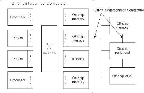
Figure 5.1 depicts a system that includes an SOC module. The SOC module typically contains a number of IP blocks, one or more of which are processors. In addition, there are various types of on-chip memory serving as cache, data, or instruction storage. Other IP blocks serving application-specific functions, such as graphics processors, video codecs, and network control units, are integrated in the SOC.
Figure 5.1 A simplified block diagram of an SOC module in a system context.
WHAT IS AN NOC?
As SOC terminology has evolved there seems to be only two interconnect strategies: the bus or the NOC. So what exactly is the NOC? Professor Nurmi (in a presentation reported by Leibson [156]) summarized the NOC characteristics:
1. The NOC is more than a single, shared bus.
2. The NOC provides point-to-point connections between any two hosts attached to the network either by crossbar switches or through node-based switches.
3. The NOC provides high aggregate bandwidth through parallel links.
4. In the NOC, communication is separate from computation.
5. The NOC uses a layered approach to communications, although with few network layers due to complexity and expense.
6. NOCs support pipelining and provide intermediate data buffering between sender and receiver.
In the context of the SOC when the designer finds that bus technology provides insufficient bandwidth or connectivity, the obvious alternative is some sort of switch. Any well-designed switched interconnect will clearly satisfy points 2, 3, 4, and 6. Point 5 is not satisfied by ad hoc switching interconnects, where the processor nodes and switching interconnect are interfaced by common, specialized design. But in the SOC, incorporating various vendor IPs ad hoc interconnects is almost never the case. The designer selects a common communications interface (layer) separate from the processor node.
The IP blocks in the SOC module need to communicate with each other. They do this through the interconnect, which is accessed through an interconnect interface unit (ICU). The ICU enables a common interface protocol for all SOC modules.
External to the SOC module are off-chip memories, off-chip peripheral devices, and mass storage devices. The cost and performance of the system, therefore, depends on both on-chip and off-chip interconnect structures.
Choosing a suitable interconnect architecture requires the understanding of a number of system level issues and specifications. These are:
1. Communication Bandwidth. The rate of information transfer between a module and the surrounding environment in which it operates. Usually measured in bytes per second, the bandwidth requirement of a module dictates to a large extent the type of interconnection required in order to achieve the overall system throughput specification.
2. Communication Latency. The time delay between a module requesting data and receiving a response to the request. Latency may or may not be important in terms of overall system performance. For example, long latency in a video streaming application usually has little or no effect on the user’s experience. Watching a movie that is a couple of seconds later than when it is actually broadcast is of no consequence. In contrast, even small, unanticipated latencies in a two-way mobile communication protocol can make it almost impossible to carry out a conversation.
3. Master and Slave. These terms concern whether a unit can initiate or react to communication requests. A master, such as a processor, controls transactions between itself and other modules. A slave, such as memory, responds to requests from the master. An SOC design typically has several masters and numerous slaves.
4. Concurrency Requirement. The number of independent simultaneous communication channels operating in parallel. Usually, additional channels improve system bandwidth.
5. Packet or Bus Transaction. The size and definition of the information transmitted in a single transaction. For a bus, this consists of an address with control bits (read/write, etc.) and data. The same information in an NOC is referred to as a packet. The packet consists of a header (address and control) and data (sometimes called the payload).
6. ICU. In an interconnect, this unit manages the interconnect protocol and the physical transaction. It can be simple or complex, including out-of-order transaction buffering and management. If the IP core requires a protocol translation to access the bus, the unit is called a bus wrapper. In an NOC, this unit manages the protocol for transport of a packet from the IP core to the switching network. It provides packet buffering and out-of-order transaction transmission.
7. Multiple Clock Domains. Different IP modules may operate at different clock and data rates. For example, a video camera captures pixel data at a rate governed by the video standard used, while a processor’s clock rate is usually determined by the technology and architectural design. As a result, IP blocks inside an SOC often need to operate at different clock frequencies, creating separate timing regions known as clock domains. Crossing between clock domains can cause deadlock and synchronization problems without careful design.
Given a set of communication specifications, a designer can explore the different bandwidth, latency, concurrency, and clock domain requirements of different interconnect architectures, such as bus and NOC. Some examples of these are given in Table 5.1. Other examples include the Avalon Bus for Altera field-programmable gate arrays (FPGAs) [10], the Wishbone Interconnect for use in open-source cores and platforms [189], and the AXI4-Stream interface protocol for FPGA implementation [74].
TABLE 5.1 Examples of Interconnect Architectures [167]

*As implemented in the ARM PL330 high-speed controller.
BW, bandwidth.
Designing the interconnect architecture for an SOC requires careful consideration of many requirements, such as those listed above. The rest of this chapter provides an introduction to two interconnect architectures: the bus and the NOC.
5.3 BUS: BASIC ARCHITECTURE
The performance of a computer system is heavily dependent on the characteristics of its interconnect architecture. A poorly designed system bus can throttle the transfer of instructions and data between memory and processor, or between peripheral devices and memory. This communication bottleneck is the focus of attention among many microprocessor and system manufacturers who, over the last three decades, have adopted a number of bus standards. These include the popular VME bus and the Intel Multibus-II. For systems on a board and personal computers, the evolution includes the instruction set architecture (ISA) bus, the EISA bus, and the now prevalent PCI and PCI Express buses. All these bus standards are designed to connect together integrated circuits (ICs) on a printed circuit board (PCB) or PCBs in a system-on-board implementation.
While these bus standards have served the computing community well, they are not particularly suited for SOC technology. For example, all such system-level buses are designed to drive a backplane, either in a rack-mounted system or on a computer motherboard. This imposes numerous constraints on the bus architecture. For a start, the number of signals available is generally restricted by the limited pin count on an IC package or the number of pins on the PCB connector. Adding an extra pin on a package or a connector is expensive. Furthermore, the speed at which the bus can operate is often limited by the high capacitive load on each bus signal, the resistance of the contacts on the connector, and the electromagnetic noise produced by such fast-switching signals traveling down a PCB track. Finally, drivers for on-chip buses can be much smaller, saving area and power.
Before describing bus operations and bus structures in detail, we provide, in Table 5.2, a comparison of two different bus interconnect architectures, showing size and speed estimates for a typical bus slave.
TABLE 5.2 Comparison of Bus Interconnect Architectures [198]
| Standard | Speed (MHz) | Area (rbe*) |
| AMBA(implementation dependent) | 166–400 | 175,000 |
| CoreConnect | 66/133/183 | 160,000 |
*rbe = register bit equivalent; estimates are approximate and vary by implementation.
5.3.1 Arbitration and Protocols
Conceptually, the bus is just wires shared by multiple units. In practice, some logic must be present to provide an orderly use of the bus; otherwise, two units may send signals at the same time, causing conflicts. When a unit has exclusive use of the bus, the unit is said to own the bus. Units can be either potentially master units that can request ownership or slave units that are passive and only respond to requests. A bus master is the unit that initiates communication on a computer bus or input/output (I/O) paths. In an SOC, a bus master is a component within the chip, such as a processor. Other units connected to an on-chip bus, such as I/O devices and memory components, are the “slaves.” The bus master controls the bus paths using specific slave addresses and control signals. Moreover, the bus master also controls the flow of data signals directly between the master and the slaves.
A process called arbitration determines ownership. A simple implementation has a centralized arbitration unit with an input from each potential requesting unit. The arbitration unit then grants bus ownership to one requesting unit, as determined by the bus protocol.
A bus protocol is an agreed set of rules for transmitting information between two or more devices over a bus. The protocol determines the following:
- the type and order of data being sent;
- how the sending device indicates that it has finished sending the information;
- the data compression method used, if any;
- how the receiving device acknowledges successful reception of the information; and
- how arbitration is performed to resolve contention on the bus and in what priority, and the type of error checking to be used.
5.3.2 Bus Bridge
A bus bridge is a module that connects together two buses, which are not necessarily of the same type. A typical bridge can serve three functions:
1. If the two buses use different protocols, a bus bridge provides the necessary format and standard conversion.
2. A bridge is inserted between two buses to segment them and keep traffic contained within the segments. This improves concurrency: both buses can operate at the same time.
3. A bridge often contains memory buffers and the associated control circuits that allow write posting. When a master on one bus initiates a data transfer to a slave module on another bus through the bridge, the data is temporarily stored in the buffer, allowing the master to proceed to the next transaction before the data are actually written to the slave. By allowing transactions to complete quickly, a bus bridge can significantly improve system performance.
5.3.3 Physical Bus Structure
The nature of the bus transaction depends on the physical bus structure (number of wire paths, cycle time, etc.) and the protocol (especially the arbitration support). Multiple bus users must be arbitrated for access to the bus in any given cycle. Thus, arbitration is part of the bus transaction. Simple arbiters have a request cycle wherein signals from the users are prioritized, followed by the acknowledge cycle selecting the user. More complex arbiters add bus control lines and associated logic so that each user is aware of pending bus status and priority. In such designs no cycles are added to the bus transaction for arbitration.
5.3.4 Bus Varieties
Buses may be unified or split (address and data). In the unified bus the address is initially transmitted in a bus cycle followed by one or more data cycles; the split bus has separate buses for each of these functions.
Also, the buses may be single transaction or tenured. Tenured buses are occupied by a transaction only during associated addresses or data cycles. Such buses have unit receivers that buffer the messages and create separate address and data transactions.
EXAMPLE 5.1 BUS EXAMPLES
There are many possible bus designs with varying combinations of physical bus widths and arbitration protocols. The examples below consider some obvious possibilities. Suppose the bus has a transmission delay of one processor cycle, and the memory (or shared cache) has a four-cycle access delay after an initial address and requires an additional cycle for each sequential data access. The memory is accessed 4 bytes at a time. The data to be transmitted consist of a 16-byte cache line. Address requests are 4 bytes.
In these examples, Taccess is the time required to access the first word from memory after the address is issued, and line access is the time required to access the remaining words. Also, the last byte of data arrives at the end of the timing template and can be used only after that point.
(a) Simple Bus. This is a single transaction bus with simple request/acknowledge (ack) arbitration. It has a physical width of 4 bytes. The request and ack signals are separate signals but assumed to be part of the bus transaction, so the bus transaction latency is 11 cycles. The first word is sent from memory at the last cycle of Taccess, while the fourth (and last) word is sent from memory at the last cycle of line access. The final bus cycle is to reset the arbiter.

(b) Bus with Arbitration Support. This bus has a more sophisticated arbiter but still has a 4-byte physical width and integrates address and data. There is an additional access cycle (five cycles instead of four) to represent the time to move the address from the bus receiver to the memory. This is not shown in case (a), as simple buses are usually slower with immediate coupling to memory. Now the initial cycles for request and ack are overlapped with bus processing, and the final cycle for resetting the arbiter is not shown in the figure for case (b), so the bus transaction now takes 10 cycles.

(c) Tenured Split Bus, 4 Bytes Wide. The assumption is that the requested line is fetched into a buffer for five cycles and then transmitted in four cycles. While the transaction latency, including the cycle for the address, is no different from that in case (b) at 10 cycles, the transaction occupies the bus for less than half (four cycles) of that time. The address bus is used for only one cycle out of 10. The remaining time is available for other unrelated transactions to improve communication performance.

(d) Tenured Split Bus, 16 Bytes Wide, with a One-Cycle Bus Transaction Time. As with case (c), the transaction latency is unaffected at 10 cycles. Since the memory clearly limits the system, in this case the memory fetches the entire 16-byte cache line before transmitting it in a single cycle. Both address and data buses are used for only one cycle per transaction. Note that the figure for case (d) allows an additional cycle to reaccess the bus, although this might not be needed and is not accounted for in case (c).

Cases (c) and (d) are interesting, since the bus bandwidth exceeds the memory bandwidth; for instance, in case (d), the memory is busy for seven cycles (four cycles to access the first word and three cycles to assess the remaining words) but the bus is busy for only one cycle. In both of these cases, the “bus”–memory situation is memory limited since that is where the contention will develop.
5.4 SOC STANDARD BUSES
Two commonly used SOC bus standards are the Advanced Microcontroller Bus Architecture (AMBA) bus developed by ARM and the CoreConnect bus developed by IBM. The latter has been adopted in Xilinx’s Virtex platform FPGA families.
5.4.1 AMBA
The AMBA, introduced in 1997, had its origin from the ARM processor, which is one of the most successful SOC processors used in the industry. The AMBA bus is based on traditional bus architecture employing two levels of hierarchy. Two buses are defined in the AMBA specification [22]:
- The Advanced High-Performance Bus (AHB) is designed to connect embedded processors, such as an ARM processor core, to high-performance peripherals, direct memory access (DMA) controllers, on-chip memory, and interfaces. It is a high-speed, high-bandwidth bus architecture that uses separate address, read, and write buses. A minimum of 32-bit data operation is recommended in the standard and data widths are extendable to 1024 bits. Concurrent multiple master/slave operations are supported. It also supports burst mode data transfers and split transactions. All transactions on the AHB bus are referenced to a single clock edge, making system-level design easy to understand.
- The Advanced Peripheral Bus (APB) has a lower performance than the AHB bus, but is optimized for minimal power consumption and has reduced interface complexity. It is designed for interfacing to slower peripheral modules.
A third bus, the Advanced System Bus (ASB), is an earlier incarnation of the AHB, designed for lower performance systems using 16/32-bit microcontrollers. It is used where cost, performance, and complexity of the AHB is not justified.
The AMBA bus was designed to address a number of issues exposed by users of the ARM processor bus in SOC integration. The goals achieved by its design are [95]:
1. Modular Design and Design Reuse. Since the ARM processor bus interface is extremely flexible, inexperienced designers could inadvertently create inefficient or even unworkable designs by using ad hoc bus and control logic. The AMBA specification encourages a modular design methodology that supports better design partitioning and design reuse.
2. Well-Defined Interface Protocol, Clocking, and Reset. AMBA specifies a low-overhead bus interface and clocking structure that is simple yet flexible. The performance of the AMBA bus is enhanced by its multimaster, split transaction, and burst mode operations.
3. Low-Power Support. One of the attractions of the ARM processor when compared with other embedded processor cores is its power efficiency. The two-level partitioning of the AMBA buses ensures energy-efficient designs in the peripheral modules, which fits well with the low-power CPU core.
4. On-Chip Test Access. AMBA has an optional on-chip test access methodology that reuses the basic bus infrastructure for testing modules that are connected to the bus.
The AHB
Figure 5.2 depicts a typical system using the AMBA bus architecture. The AHB forms the system backbone bus on which the ARM processor, the high-bandwidth memory interface and random-access memory (RAM), and the DMA devices reside. The interface between the AHB bus and the slower APB bus is through a bus bridge module.
Figure 5.2 A typical AMBA bus-based system [95].

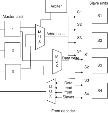
The AMBA AHB bus protocol is designed to implement a multimaster system. Unlike most bus architectures designed for PCB-based systems, the AMBA AHB bus avoids tristate implementation by employing a central multiplexer interconnect scheme. This method of interconnect provides higher performance and lower power than using tristate buffers. All bus masters assert the address and control signals, indicating the type of transfer each master requires. A central arbiter determines which master has its address and control signal routed to all the slaves. A central decoder circuit selects the appropriate read data and response acknowledge signal from the slave that is involved in the transaction. Figure 5.3 depicts such a multiplexer interconnect scheme for a system with three masters and four slaves.
Figure 5.3 Multiplexor (MUX) interconnection for a three masters/four slaves system [22].
Transactions on the AHB bus involve the following steps:
- Bus Master Obtains Access to the Bus. This process begins with the master asserting a request signal to the arbiter. If more than one master simultaneously requests the control of the bus, the arbiter determines which of the requesting masters will be granted the use of the bus.
- Bus Master Initiates Transfer. A granted bus master drives the address and control signals with the address, direction, and width of the transfer. It also indicates whether the transaction is part of a burst in the case of burst mode operation. A write data bus operation moves data from the master to a slave, while a read data bus operation moves data from a slave to the master.
- Bus Slave Provides a Response. A slave signals to the master the status of the transfer such as whether it was successful, if it needs to be delayed, or that an error occurred.
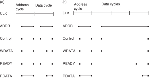
Figure 5.4a depicts a basic AHB transfer cycle. An AHB transfer consists of two distinct phases: the address phase and the data phase. The master asserts the address (ADDR) and control signals on the rising edge of the clock (CLK) during the address phase, which always lasts for a single cycle. The slave then samples the address and control signals and responds accordingly during the data phase to a data read (RDATA) or write (WDATA) operation, and indicates its completion with the READY signal. A slave may insert wait states into any transfer by delaying the assertion of READY as shown in Figure 5.4b. For a write operation, the bus master holds the data stable throughout the extended data cycles. For a read transfer the slave does not provide valid data until the last cycle of the data phase.
Figure 5.4 A simple AHB transfer [22]. (a) No wait states in transfer; (b) with wait states during transfer.
The AHB bus is a pipelined (tenured) bus. Therefore, the address phase of any transfer can occur during the data phase of a previous transfer. This overlapping pipeline feature allows for high-performance operation.
The APB
The APB is optimized for minimal power and low complexity instead of performance. It is used to interface to peripherals, which are low bandwidth.
The operation of the APB is straightforward and can be described by a state diagram with three states. The APB either stays in the Idle state, or loops around the Setup state and the Enable state during data transfer.
5.4.2 CoreConnect
As in the case of AMBA bus, IBM’s CoreConnect Bus is an SOC bus standard designed around a specific processor core, the PowerPC, but it is also adaptable to other processors. The CoreConnect Bus and the AMBA bus share many common features. Both have a bus hierarchy to support different levels of bus performance and complexity. Both have advanced bus features such as multiple master, separate read/write ports, pipelining, split transaction, burst mode transfer, and extendable bus width.
The CoreConnect architecture provides three buses for interconnecting cores, library macros, and custom logic:
- processor local bus (PLB),
- on-chip peripheral bus (OPB),
- device control register (DCR) bus.
Figure 5.5 illustrates how the CoreConnect architecture can be used in an SOC system built around a PowerPC. High-performance, high-bandwidth blocks such as the PowerPC 440 CPU core, the PCI-X bus bridge, and the PC133/DDR133 (DDR1 with a 133 MHz bus) synchronous dynamic RAM (SDRAM) Controller are connected together using the PLB, while the OPB hosts lower data rate on-chip peripherals. The daisy-chained DCR bus provides a relatively low-speed datapath for passing configuration and status information between the PowerPC 440 CPU core and other on-chip modules.
Figure 5.5 A CoreConnect-based SOC [123].

The PLB
The PLB is used for high-bandwidth, high-performance, and low-latency interconnections between the processors, memory, and DMA controllers [123]. It is a fully synchronous, split transaction bus with separate address, read, and write data buses, allowing two simultaneous transfers per clock cycle. All masters have their own Address, Read Data, Write Data, and control signals called transfer qualifier signals. Bus slaves also have Address, Read Data, and Write Data buses, but these buses are shared.
PLB transactions, as in the AMBA AHB, consist of multiple phases that may last for one or more clock cycles, and involve the address and data buses separately. Transactions involving the address bus have three phases: request (RQ), transfer (XFER), and address acknowledge (ACK). A PLB transaction begins when a master drives its address and transfer qualifier signals and requests ownership of the bus during the request phase of the address tenure. Once the PLB arbiter grants bus ownership, the master’s address and transfer qualifiers are presented to the slave devices during the transfer phase. The address cycle terminates when a slave latches the master’s address and transfer qualifiers during the address acknowledge phase.
Figure 5.6 illustrates two deep read and write address pipelining along with concurrent read and write data tenures. Master A and Master B represent the state of each master’s address and transfer qualifiers. The PLB arbitrates between these requests and passes the selected master’s request to the PLB slave address bus. The trace labeled Address Phase shows the state of the PLB slave address bus during each PLB clock.
Figure 5.6 PLB transfer protocol [123].
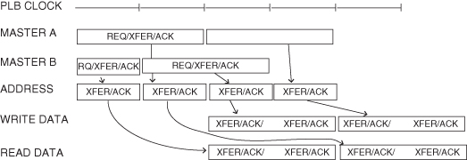
Each data beat in the data tenure has two phases: transfer and acknowledge. During the transfer phase the master drives the write data bus for a write transfer or samples the read data bus for a read transfer. As shown in Figure 5.6, the first (or only) data beat of a write transfer coincides with the address transfer phase.
Split Transaction
The PLB address, read data, and write data buses are decoupled, allowing for address cycles to be overlapped with read or write data cycles, and for read data cycles to be overlapped with write data cycles. The PLB split bus transaction capability allows the address and data buses to have different masters at the same time. Additionally, a second master may request ownership of the PLB, via address pipelining, in parallel with the data cycle of another master’s bus transfer. This situation is illustrated in Figure 5.6, with the dependence of various signals indicated by arrows.
The OPB
The OPB is a secondary bus designed to alleviate system performance bottlenecks by reducing capacitive loading on the PLB [126]. Peripherals suitable for attachment to the OPB include serial ports, parallel ports, UARTs, GPIO (general purpose I/O), timers, and other low-bandwidth devices. The OPB is more sophisticated than the AMBA APB. It supports multiple masters and slaves by implementing the address and data buses as a distributed multiplexer. This type of structure is suitable for the less data-intensive OPB bus and allows peripherals to be added to a custom core logic design without changing the I/O on either the OPB arbiter or existing peripherals. Figure 5.7 shows one method of structuring the OPB address and data buses. Both masters and slaves provide enable control signals for their outbound buses. By requiring that each unit provide this signal, the associated bus combining logic can be strategically placed throughout the chip. As shown in the figure, either of the masters is capable of providing an address to the slaves, whereas both masters and slaves are capable of driving and receiving the distributed data bus.
Figure 5.7 The on-chip peripheral bus (OPB) [126].

Table 5.3 shows a comparison between the AMBA and CoreConnect bus standards.
TABLE 5.3 Comparison between CoreConnect and AMBA Architectures [198]
| IBM CoreConnect PLB | ARM AMBA 2.0 AMBA High-Performance Bus | |
| Bus architecture | 32, 64, and 128 bits, extendable to 256 bits | 32, 64, and 128 bits |
| Data buses | Separate read and write | Separate read and write |
| Key capabilities | Multiple bus masters | Multiple bus masters |
| Four-deep read pipelining, two-deep write pipelining | Pipelining | |
| Split transactions | Split transactions | |
| Burst transfers | Burst transfers | |
| Line transfers | Line transfers | |
| OPB | AMBA APB | |
| Masters supported | Supports multiple masters | Single master: The APB bridge |
| Bridge function | Master on PLB or OPB | APB master only |
| Data buses | Separate read and write | Separate or three-state |
5.4.3 Bus Interface Units: Bus Sockets and Bus Wrappers
Using a standard SOC bus for the integration of different reusable IP blocks has one major drawback. Since standard buses specify protocols over wired connections, an IP block that complies with one bus standard cannot be reused with another block using a different bus standard. One approach to alleviate this is to employ a hardware “socket,” which is an example of a bus wrapper in Section 5.2, to separate the interconnect logic from the IP core using a well-defined IP core protocol that is independent of the physical bus protocol. Core-to-core communication is therefore handled by the interface wrapper. This approach is taken by the Virtual Socket Interface Alliance (VSIA) [44] with their virtual component interface (VCI) [249], and by Sonics Inc. employing the Open Core Protocol (OCP) and Silicon Backplane μNetwork [225].
VSIA proposes a set of standards and interfaces known as virtual socket interface (VSI) that enables system-level interaction on a chip using predesigned blocks (called virtual components [VCs]) [249]. This encourages designs using a component paradigm. The VCs, which are effectively IP blocks that conform to the VSI specifications, can be one of three varieties. Hard VCs consist of placed and routed gates with all silicon layers defined. It has predictable performance, area usage, and power consumption, but offers no flexibility. Soft VCs are designed in some hardware description language representation, which are mapped to physical design through synthesis, placement, and routing. They can be easily modified but generally take more effort to integrate and verify in the SOC design as well as having less predictable performance. Finally, firm VCs offer a compromise between the two. They come in the form of generators or partially placed library blocks that require final routing and/or placement adjustment. This form of VCs provides more predictable performance than soft VCs, but still offers some degree of flexibility in aspect ratio and configuration.
In order to connect these different VCs together, VSIA has developed a VCI specification to which other proprietary buses can interface. By following the VCI specification, a designer can take a VC and integrate it with any of several buses in order to meet system performance requirements. The VCI standard specifies a family of protocols. Currently three protocols are defined: the peripheral VCI (PVCI), the basic VCI (BVCI), and the advanced VCI (AVCI) [249]. The PVCI is a low-performance protocol where the request and the response data transfer occur during a single control handshake transaction. It is therefore not a split-transaction protocol. The BVCI employs a split-transaction protocol, but responses must arrive in order. In other words, the response data must be supplied in the same order in which the initiator generated the requests. The AVCI is similar to the BVCI, but out-of-order transactions are allowed. Requests are tagged and transactions can be interleaved and reordered.
In addition to the specification of the VCI, VSIA also specifies a number of abstraction layers to define the representation views required to integrate a VC into an SOC design [44]. The idea is that if both the IP block provider (VC provider) and the system integrator (VC integrator) conform to the VSI specifications at all levels of abstraction, SOC designs using an IP component paradigm can proceed with lower risk of errors.
An alternative to VCI is the OCP promoted by the Open Core Protocol International Partnership (OCP-IP) [188]. The OCP defines a point-to-point interface between two communicating entities such as two IP cores using a core-centric protocol. An interface implementing the OCP assumes the attributes of a socket, which, as explained earlier, is effectively a bus wrapper that allows interfacing to the target bus. A system consisting of three IP core modules using the OCP and bus wrappers is shown in Figure 5.8. One module is a system initiator, one is a system target, and another is both initiator and target.
Figure 5.8 A three-core system using OCP and bus wrappers [225].

Another layer of interconnection can be made above the OCP in order to help IP integration further. Sonics Inc. proposes their proprietary SiliconBackplane Protocol that seamlessly glues together IP blocks that uses the OCP. The communication between different blocks takes place over the Silicon Backplane μNetwork, which has a scalable bandwidth of 50–4000 MB/s. Figure 5.9 depicts how the Sonics μNetwork components are connected together [225].
Figure 5.9 Sonics μNetwork configuration [225]. DSP, digital signal processor.

Bus interface units using the wrapper-based approach have been demonstrated to reduce the design time of SOC, but at a cost in terms of gates and latency. Attaching simple wrapper hardware increases the access latencies and incurs a hardware overhead of 3–5 K gates [160].
In addition, bus interface units can include first-in–first-out (FIFO) buffers to improve performance. Figure 5.10 shows the amount of hardware overhead incurred and performance improvement achieved by employing write data buffers in a bus interface unit [9].
Figure 5.10 (a) Hardware overhead of write buffers; (b) performance impact of buffer for burst mode transfer [9].
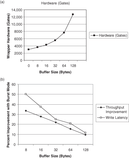
The write buffer provides several cycles improvement in latency and, depending on the data size, more than 10% improvement in throughput.
5.5 ANALYTIC BUS MODELS
5.5.1 Contention and Shared Bus
Contention occurs wherever two or more units request a shared resource that cannot supply both at the same time. When contention occurs, either (1) it delays its request and is idle until the resource is available or (2) it queues its request in a buffer and proceeds until the resource is available. Case (2) is only possible when the requested item is not logically essential to program execution (as in a cache prefetch, for example).
Whether we need to analyze the bus as a source of contention depends on its maximum (or offered) bandwidth relative to the memory bandwidth. As contention and queues develop at the “bottleneck” in the system, the most limiting resource is the source of the contention, and other parts of the system simply act as delay elements. Thus buses must be analyzed for contention when they are more restrictive (have less available bandwidth) than memory.
Buses often have no buffering (queues), and access delays cause immediate system slowdown. The analysis on the effects of bus congestion depends on the access type and buffering.
Generally there are two types of access patterns:
1. Requests without Immediate Resubmissions. The denied request returns with the same arrival distribution as the original request. Once a request is denied, processing continues despite the delay in the resubmission of the request. This is the case of a cache line prefetch, which is not currently required for continued program execution.
2. Requests Are Immediately Resubmitted. This is a more typical case, when multiple independent processors access a common bus. A program cannot proceed after a denied request. It is immediately resubmitted. The processor is idle until the request is honored and serviced.
5.5.2 Simple Bus Model: Without Resubmission
In the following, we assume that each request occupies the bus for the same service time (e.g., Tline access). Even if we have two different types of bus users (e.g., word requests and line requests on a single line or [dirty] double line requests), most cases are reasonably approximated by simple computation of the per-processor average (offered) bus occupancy, ρ, given by:
![]()
The processor time is the mean time the processor needs to compute before making a bus request. Of course, it is possible for the processor to overlap some of its compute time with the bus time. In this case, the processor time is the net nonoverlapped time between bus requests. In any event, ρ ≤ 1.
The simplest model for n processors accessing a bus is given by:
![]()
![]()
The fraction of bandwidth realized times the maximum bus bandwidth gives the realized (or achieved) bus bandwidth, Bw.
The achieved bandwidth fraction (achieved occupancy) per processor (ρa) is given by:

A processor slows down by ρa/ρ due to bus congestion.
5.5.3 Bus Model with Request Resubmission
A model that supports request resubmission involves a more complex analysis and requires an iterative solution. There are several solutions, each providing similar results. The solution provided by Hwang and Briggs [122] is an iterative pair of equations:
![]()
and
![]()
where a is the actual offered request rate. To find a final ρa, initially set a = ρ to begin the iteration. Convergence usually occurs within four iterations.
5.5.4 Using the Bus Model: Computing the Offered Occupancy
The model in the preceding section does not distinguish among types of transactions. It just requires the mean bus transaction time, which is the average number of cycles that the bus is busy managing a transaction. Then the issue is finding the offered occupancy, ρ.
The offered occupancy is the fraction of the time that the bus would be busy if there were no contention among transactions (bounded by 0.0 and 1.0). In order to find this, we need to determine the mean time for a bus transaction and the compute time between transactions.
The nature of the processor initiating the transaction is another factor. Simple processors make blocking transactions. In this case the processor is idle after the bus request is made and resumes computation only after the bus transaction is complete. The alternative for more complex processors is a buffered (or nonblocking) transaction. In this case the processor continues processing after making a request, and may indeed make several requests before completion of an initial request. Depending on the system configuration, there are two common cases:
1. A Single Bus Master with Blocking Transactions. In this case there is no bus contention as the processor waits for the transaction to complete. Here the achieved occupancy, ρa, is the same as the offered occupancy, and ρ = ρa = (bus transaction time)/(compute time + bus transaction time).
2. Multiple (n) Bus Masters with Blocking Transactions. In this case the offered occupancy is simply nρ where ρ is as in case (1). Now contention can develop so we use our bus model to determine the achieved occupancy, ρa.
Example. Suppose a processor has bus transactions that consist of cache line transfers. Assume that 80% of the transactions move a single line and occupy the bus for 20 cycles and 20% of the transactions move a double line (as in dirty line replacement), which takes 36 cycles. The mean bus transaction time is 23.2 cycles. Now assume that a cache miss (transaction) occurs every 200 cycles.
In case (1), the bus is occupied: ρ = ρa = 23.2/223.2 = 0.10; there is no contention, but the bus causes a system slow down, as discussed below.
In case (2), suppose we have four processors. Now the offered occupancy is ρ = 0.104 and we use our model to find the contention time. Initially we set a = ρ = 0.104, nρa = 1 − (1 − a)n = 1 − (1 − 0.104)4; now we find ρa and substitute the value of ρa for a and continue.
So initially, ρa = 0.089; after the next iteration, ρa = 0.010; and after several iterations, ρa = 0.095. We always achieve less than what is offered and the difference is delay due to contention. So:
![]()
Solving for the contention time, we get about 21 cycles.
5.5.5 Effect of Bus Transactions and Contention Time
There are two separate effects of bus delays on overall system performance. The first is the obvious case of blocking, which simply inserts a transaction delay into the program execution. The second effect is due to contention. Contention reduces the rate of transaction flow into the bus and memory. This reduces performance proportionally.
In the case of blocking the processor simply slows down by the amount of the bus transaction. So the relative performance compared to an ideal processor with no bus transactions is:
![]()
In the case (1) example the processor slows down by 200/223.3 = 0.896.
Contention, when present, adds additional delay. In case (2) the individual processor slows down by 200/(223.2 + 21) = 0.819. The result of contention is that it simply slows down the system (without contention) by the ratio of ρa/ρ. The supply of transactions is reduced by this ratio.
5.6 BEYOND THE BUS: NOC WITH SWITCH INTERCONNECTS
While bus interconnect has been the predominant architecture for SOC interconnections, it suffers from a number of drawbacks. Even a well-designed bus-based system may suffer from data transfer bottlenecks, limiting the performance of the entire system. It is also not inherently scalable. As more modules are added to a bus, not only does data congestion increase, but power consumption also rises due to the increased load presented to the bus driver circuits. Switch-based NOC interconnections avoid some of these limitations. However, switches are inherently more complex than buses and are most useful in larger SOC configurations. There are broad trade-offs possible in switch design. Large numbers of nodes can be interconnected with relatively low latency but at exponentially increasing cost (as with crossbar switches) or they can be implemented with relatively longer latency and with more modest cost (as in a distributed interconnection).
This section presents some basic concepts and alternatives in the design of the physical interconnect network. This network consists of a configuration of switches to enable the interconnection of N units. The design efficiency or cost–performance of the interconnection network is determined by:
1. The delay in connecting a requesting unit to its destination.
2. The bandwidth between units and the number of connections that can be carried on concurrently.
3. The cost of the network.
SOC INTERCONNECT SWITCHES.
This section is an abstract of some of the basic concepts and results from the computer interconnect literature. In SOC switching, currently the number of nodes (units) is typically limited by die size to 16–64. Since the units are on chip, the link bandwidth, w, is relatively large: 16–128 wires. In SOC, dynamic networks are dominant so far (either crossbar or multistage); static networks, when used, tend to be a grid (torus). As the number of SOC units increases, a greater variety of network implementations are expected.
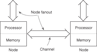
In a network, units communicate with one another via a link or a channel, which can be either unidirectional or bidirectional. Links have bandwidth or the number of bits per unit time that can be transmitted concurrently between units (or nodes). The fanout of a node is the number of bidirectional channels connecting it to its neighboring nodes (Figure 5.11).
Figure 5.11 Node and channels; the node fanout is the number of channels connecting a node to its neighbors.
Networks can be static or dynamic. In a static network, the topology or the relationship between nodes in the network is fixed (Figure 5.12). The path between two nodes does not change. In a dynamic network, the paths between nodes can be altered both to establish connectivity and also to improve network bandwidth (Figure 5.13).
Figure 5.12 Static network (links between units is fixed).

Figure 5.13 Dynamic network (links between units vary to establish connection).
A static network could consist of a 2-D grid of switches [64] to connect together SOC modules. A dynamic network could consist of a centralized crossbar switch. Apart from the advantage of avoiding traffic congestion, a switch-based scheme may allow modules to operate at different clock frequencies as well as alleviating the bus loading problem.
Figure 5.14 shows a crossbar-based interconnect that connects some locally synchronous blocks on the same chip [66]. The crossbar switch is fully asynchronous. Inside the chip, clock domain converters are used to bridge the asynchronous interconnect to the synchronous blocks.
Figure 5.14 A switch-based interconnect scheme [66].

5.6.1 Static Networks
In a static network the distance between two units is the smallest number of links or channels (or hops) that must be traversed for establishing communications between them. The diameter of the network is the largest distance (without backtracking) between any two units in the network. An example of a static network in a linear network is found in Figure 5.15a. Networks can be open or closed. A closed network improves average distance and diameter by converting a linear array into a ring (Figure 5.15b). The most common type of static network is the (k, d) network [70]. This is a regular array of nodes with dimension d and with k nodes in each dimension. These networks are usually closed as in the case of a ring, d = 1 or a torus, d = 2.
Figure 5.15 Example of static network without preferred sites. (a) Linear array; (b) linear array with closure (a ring); (c) grid (2-D mesh); (d) k × k grid with closure (a 2-D torus). These are also called (k, d) networks. In (a) and (b), we have k = 4, d = 1 (one dimensional). In (c) and (d), we have k = 3, d = 2.
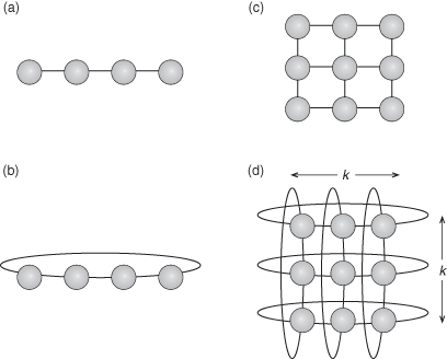
Assume there are k nodes in a linear array and we wish to extend the network. Instead of simply increasing the number of linear elements, we can increase the dimensionality of the network, creating a grid network of two dimensions, d = 2 (Figure 5.15c). These (k, d) networks can be linear arrays, d = 1, 2-D grids, d = 2, cubic arrays, d = 3, or hypercubes. Hypercubes are usually limited to two elements per dimension, k = 2, with as many dimensions as needed to contain the network. Higher dimensional networks improve the connectivity but at the expense of connection switches. There must be a switch for each nearest neighbor and generally there are 2d neighbors in a (k, d) network. Figure 5.15d represents a torus, commonly referred to as a nearest-neighbor mesh.
In the special case of the binary cube, or hypercube, k = 2. The number of hypercube nodes (N) and the diameter can be determined as follows: for (2, n), the binary n-cube with bidirectional channels has:
![]()
and for the (2, n) case:
![]()
For general (k, n) with n dimensions and with closure and bidirectional channels, we have
![]()
or
![]()
and
![]()
Example. Suppose we have a 4 × 4 grid (torus as in Figure 5.15d). In (k, d) terms it is a (4, 2) network, N = 16 and n = 2, and the diameter is 4.
In general, it is the dimension of the network and its maximum distance that are important to cost and performance. Some cost and performance comparisons for various (k, d) static networks are shown in Table 5.4.
TABLE 5.4 Some Cost and Performance Comparisons for Various (k, d) Static Networks with 64 Nodes (N = 64)
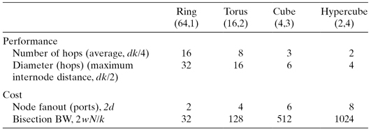
Links (and ports) are bidirectional with 16 wires (w = 16). Bisection bandwidth (BW) refers to the number of wires intersected when a network is split into two equal halves.
Links are characterized in three ways:
1. The Cycle Time of the Link, Tch. This corresponds to the time it requires to transmit between neighboring nodes. 1/Tch is the bandwidth of a wire in the link or channel.
2. The Width of the Link, w. This determines the number of bits that may be concurrently transmitted between two nodes.
3. Whether the link is unidirectional or bidirectional.
Associated with the link characterization is the length of the message in bits (l) plus H header bits. The header is simply the address of the destination node. Thus, Tch × (l + H)/w will be the time required to transmit a message between two adjacent units.
Suppose unit A has a message for unit C, which must be transmitted via unit B. If node B is available, the message is transmitted first from A to B and stored at B. After the message has been completely transmitted, node B accesses node C and transmits the message to C if C is available. Rather than storing the message at B, we can use wormhole routing [70]. As the message is received at B, it is buffered only long enough to decode its header and determine its destination. As soon as this minimal amount of information can be determined, the message is retransmitted to C, assuming that C is available. The amount of buffering then required at B is significantly reduced and the overall time of transmission is:
![]()
where h = [H/w].
Example. In a 4 × 4 grid, (k, d) = (4, 2) and, assuming Tch = 1, let h = 1, l = 256 and w = 64. Then Twormhole = 2 + 4 = 6 cycles.
Once the header is decoded at an intermediate node, that node can determine whether the message is for it or for another node. The intermediate node selects a minimum distance path to the destination node. If multiple paths have the same distance, then this intermediate node will select the path that is currently unblocked or available to it.
5.6.2 Dynamic Networks
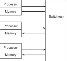
The dynamic indirect network is shown in Figure 5.16a and b.
Figure 5.16 A basic dynamic, indirect switching network. P, processor; M, memory. Figure 5.16a represents a centralized switching network, separate from the processors. Figures 5.16b shows a more distributed network.

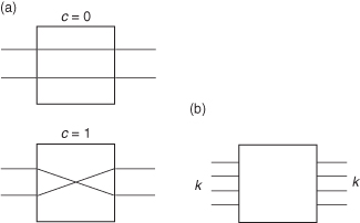
Typically, the basic element in the dynamic network is a crossbar switch (Figure 5.17).
Figure 5.17 (a) A 2 × 2 crossbar with control c; (b) this can be generalized to a k × k crossbar switch.
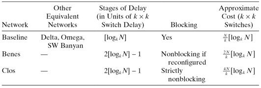
The crossbar simply connects one of k points to any of another k points. Multiple messages can be concurrently executed across the crossbar switch, so long as two messages do not have the same destination. The cost of the crossbar switch increases as n2, so that for larger networks, use of a crossbar switch only becomes prohibitively expensive. In order to contain the cost of the switch, we can use a small crossbar switch as the basis of a multistage network, frequently referred to as a MIN—multistage interconnection network [256]. There are many types, including baseline, Benes, Clos, Omega [150], and Banyan networks. The baseline network is among the simplest, and is shown in Figure 5.18.
Figure 5.18 Baseline dynamic network topology.

The header causes successive stages of the switch to be set so that the proper connection path is established between two nodes. For example, consider a deterministic “obvious” routing algorithm for these M, N networks. Suppose node 011 sends a message to destination 110. The switch outputs labeled 1, 1, and 0 cause the message to be routed to the 110 destination node by setting the control (c) so that either the upper output (“0”) or the lower output (“1”) of each switch is selected. Similarly, the return path is simply 011. The number of stages between two nodes is:
![]()
where k is the number of inputs to the crossbar element (k × k) and therefore the total number of (k × k) switches required for a one-bit wide path is:
![]()
Other dynamic networks provide different trade-offs on achievable message bandwidth, message delay, and fault tolerance. Table 5.5 summarizes some of the attributes of some common dynamic networks.
TABLE 5.5 Dynamic Networks, Switching N Inputs × N Outputs Using k × k Switches
5.7 SOME NOC SWITCH EXAMPLES
5.7.1 A 2-D Grid Example of Direct Networks
Data traffic can be distributed over the entire NOC by connecting the user IP cores through a direct interconnect network. Data transfer bottlenecks are avoided because there are multiple paths between nodes and data transfers can be performed simultaneously. Xfabric uses a 2-D grid direct network approach to connect user cores on a Xilinx FPGA as shown in Figure 5.19 [64]. Data processing cores with one to four communication ports are interconnected via a network of junction components (shown in gray). These data routing junctions manage system data flow autonomously between multiple user cores. Multiple instances of junctions form a direct two-dimensional grid network that can interconnect up to 1024 single-port cores. Horizontal and vertical data transport links between junction components enable efficient data communications between cores.
Figure 5.19 Xfabric connecting data processing core via junction components [64]. It is a direct switching network using a 2-D grid topology.
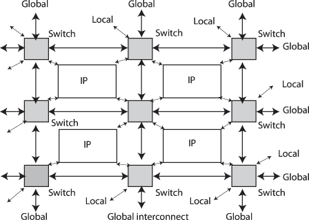
Figure 5.20 shows the functional schematic of a junction component. Each junction consists of four Local Ports (from LPORT0 to LPORT3) and four Global Ports (from GPORT0 to GPORT3). User cores send 48-bit words and receive 32-bit words via Local Ports, while the 16-bit Global Ports are used to route data to adjacent junctions.
Figure 5.20 Schematic diagram of a junction component [64].

Each junction component performs all the necessary routing and arbitration functions to deliver multiple parallel data streams between data sources and destinations with minimum latency, thus avoiding transfer bottlenecks found in bus-based systems.
5.7.2 Asynchronous Crossbar Interconnect for Synchronous SOC (Dynamic Network)
Another NOC for SOC applications is the PivotPoint architecture by Fulcrum [66]. The center of the system is the Nexus crossbar switch (see Figure 5.14), which has a data throughput rate of 1.6 Tbps. Nexus uses clockless asynchronous circuits and has the advantages normally associated with this design style, including adaptivity to process technology, environmental variations, and lower system power consumption. The choice of asynchronous design style is partly driven by the need for interconnecting multiple clock domain cores. The synchronous cores can run at different frequencies with independent phase relationships to each other. Clock-domain converters are required to interface between the synchronous cores and the asynchronous crossbar. Since the crossbar switch does not use any clock signals, integrating different clock domains require no extra effort. In this way, the system is globally asynchronous, but locally synchronous, which is also known as a GALS system.
Data transfer on Nexus is done through bursts. Each burst contains a variable number of data words (36-bit) and is terminated by a tail signal. A 4-bit control is used to indicate a destination channel (TO), which becomes the source channel (FROM) when the burst leaves the crossbar. The format of the burst is shown in Figure 5.21. Bursts are automatically routed by the crossbar and cannot be dropped, fragmented, or duplicated.
Figure 5.21 Format of burst used on Nexus [66].
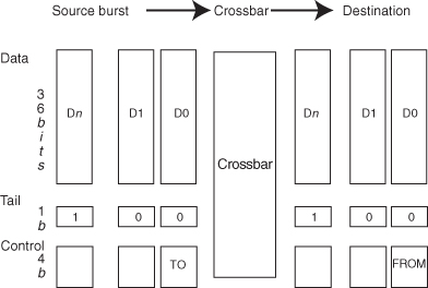
The crossbar provides the routing through a physical link that is created when the first word of the burst enters the crossbar and is closed when the last word leaves the crossbar.
5.7.3 Blocking versus Nonblocking
Nexus and PivotPoint are designed to avoid head-of-the-line (HOL) blocking. HOL blocking occurs when one packet failing to progress results in other unrelated packets behind it to be blocked. PivotPoint uses virtual channels (also called ports) to transport separated traffic streams simultaneously. Blocked packets in one channel only blocks packets behind it on the same channel. Packets on other channels are free to progress. In this way communication stalls are minimized.
5.8 LAYERED ARCHITECTURE AND NETWORK INTERFACE UNIT
The network interface unit is a key component in the NOC, since it can overcome a number of limitations found in the conventional bus-based approach [40]. Although the bus standards discussed earlier provide some degree of portability and reusability of IP cores, they are difficult to adapt to advances in both process and bus interface technologies. The fundamental weakness of buses is that they do not take a layered approach to interconnection: There is no explicit separation between the transaction level communication in the application layer and the interconnect signals in the physical layer. In contrast, activities in NOC systems are generally separated into transaction, transport, and physical layers as depicted in Figure 5.22. As a result, NOC systems can be adapted more easily to the rapid advances in process technology or in system architecture.
Figure 5.22 The layered architecture of NOC [26].

Figure 5.23 shows a general-purpose on-chip interconnect network comprising of a number of modules such as processors, memories, and IP blocks organized as tiles. These module tiles are connected to the network that routes packets of data between them. All communications between tiles are via the network, and the area overhead of the network logic can be as low as 6.6% [71]. The key characteristics of such NOC architectures are that they have: (1) a layered architecture that is easily scalable; (2) a flexible switching topology that can be configured by the user to optimize performance for different applications; and (3) point-to-point communication that effectively decouples the IP blocks from each other.
Figure 5.23 A typical NOC architecture [26].
5.8.1 NOC Layered Architecture
Most NOC architectures adopt a three-layered communication scheme, as shown in Figure 5.22. The physical layer specifies how packets are transmitted over the physical interfaces. Any changes in process technology, interconnecting switch structure, and clock frequency affect only this layer. Upper layers are not compromised in any way.
The transport layer defines how packets are routed through the switch network. A small header cell in the packet is typically used to specify how routing is to be done. The transaction layer defines the communication primitives used to connect the IP blocks to the network. The NOC interface unit (NIU) provides the transaction level services to the IP block, governing how information is exchanged between NIUs to implement a particular transaction (Figure 5.24).
Figure 5.24 The transaction, transport, and physical layers of an NOC [26].

The layered architecture of NOC offers a number of benefits [26]:
1. Physical and Transport Layers can be Independently Optimized. The physical layer is governed mostly by process technology while the transaction layer is dependent on the particular application. The layered approach allows them to be separately optimized without affecting each other.
2. Inherently Scalable. A properly designed switch fabric in an NOC can be scaled to handle any amount of simultaneous transactions. The distributed nature of the architecture allows the switches to be optimized to match the requirements. At the same time, the NIU responsible for the transaction layer can be designed to satisfy the performance requirement of the IP block that it services with no effect on the configuration and performance of the switch fabric.
3. Better Control of Quality-of-Service. Rules defined in the transport layer can be used to distinguish between time-critical and best-effort traffic. Prioritizing packets helps to achieve quality-of-service requirements enabling real-time performance on critical modules.
4. Flexible Throughput. By allocating multiple physical transport links, throughput can be increased to meet the demand of a system statically or dynamically.
5. Multiple Clock Domain Operation. Since the notion of a clock only applies to the physical layer and not to the transport and transaction layers, an NOC is particularly suited to an SOC system containing IP blocks that operate at different clock frequencies. Using suitable clock synchronization circuits at the physical layer, modules with independent clock domains can be combined with reduced timing convergence problems.
5.8.2 NOC and NIU Example
For the Nexus crossbar switch in Section 5.7.2, the NIU implements the PivotPoint system architecture connecting nodes using the Nexus crossbar switch. Figure 5.25 shows a simplified PivotPoint architecture. In addition to the Nexus crossbar switch, the FIFO buffer provides data-buffering function for the transmit (TX) and the receive (RX) channels. The System Packet Interface (SPI-4.2, represented simply as SPI-4 in the figure) implements a standard protocol for chip-to-chip communication at data rates of 9.9–16 Gbps.
Figure 5.25 PivotPoint architecture [66].

5.8.3 Bus versus NOC
When compared with buses, NOC is not without drawbacks. Perhaps the most significant weakness of NOC is the extra latency that it introduces. Unlike data communication networks, where quality of service is governed mainly by bandwidth and throughput, SOC applications usually also have very strict latency constraints. Furthermore, the NIU and the switch fabric add to the area overhead of the system. Therefore, direct implementation of a conventional network architecture in SOC generally results in unacceptable area and latency overheads. Table 5.6 presents the pros and cons between buses and NOC approaches to SOC interconnect qualitatively.
TABLE 5.6 The Bus-versus-NOC Arguments [112]
| Bus Pros and Cons | NOC Pros and Cons |
| Every unit attached adds parasitic capacitance (−) | Only point-to-point one-way wires are used for all network sizes (+) |
| Bus timing is difficult in deep submicron process (−) | Network wires can be pipelined because the network protocol is globally asynchronous (+) |
| Bus testability is problematic and slow (−) | Built-in self-test (BIST) is fast and complete (+) |
| Bus arbiter delay grows with the number of masters. The arbiter is also instance specific (−) | Routing decisions are distributed and the same router is used for all network sizes (+) |
| Bandwidth is limited and shared by all units attached (−) | Aggregated bandwidth scales with the network size (+) |
| Bus latency is zero once arbiter has granted control (+) | Internal network contention causes a small latency (−) |
| The silicon cost of a bus is low for small systems (+) | The network has a significant silicon area (−) |
| Any bus is almost directly compatible with most available IPs, including software running on CPUs (+) | Bus-oriented IPs need smart wrappers. Software needs clean synchronization in multiprocessor systems (−) |
| The concepts are simple and well understood (+) | System designers need re-education for new concepts (−) |
5.9 EVALUATING INTERCONNECT NETWORKS
There have been a number of important analyses about the comparative merits of various network configurations [137, 145, 194]. The examples below illustrate the use of simple analytic models in evaluating interconnect networks.
5.9.1 Static versus Dynamic Networks
In this section, we present the results and largely follow the analyses performed by Agarwal [8] in his work on network performance.
Dynamic Networks
Assume we have a dynamic indirect network made up of k × k switches with wormhole routing. Let us assume this network has n stages and channel width w with message length l. In the indirect network, we assume that the header network path address is transmitted in one cycle just before the message leaves the node, so that there is only one cycle of header overhead to set up the interconnect; see Figure 5.26.
Figure 5.26 Message transmission from node to switch.

Assuming the switches have unit delay (Tch = one cycle), the total time for a message to transit the network without contention is:
![]()
For all our subsequent analysis we assume that n + l/w ![]() 1, so
1, so
![]()
In a blocking dynamic network, each network switch has a buffer. If a block is detected, a queue develops at the node; so each of N units with occupancy ρ requests service from the network. Since the number of connection lines at each network level is the same (N), then the expected occupancy for each is ρ. At each switch, the message transmits experiences a waiting time. Kruskal and Snir [145] have shown that this waiting time is (assume that Tch = 1 cycle and express time in cycles):
![]()
The channel occupancy is
![]()
where m is the probability that a node makes a request in a channel cycle.
The total message transit time, Tdynamic, is:

Static Networks
A similar analysis may be performed on a static (k, n) network. Let kd be the average number of hops required for a message to transit a single dimension. For a unidirectional network with closure ![]() and for a bidirectional network
and for a bidirectional network ![]() , the total time for a message to pass from source to destination is:
, the total time for a message to pass from source to destination is:
![]()
Again, we assume that Tch = 1 cycle and perform the remaining computations on a cycle basis. Agarwal [8] computes the waiting time (M/G/1) as:
![]()
The total transit time for a message to a destination (h = 1) is:
The preceding cannot be used for low k (i.e., k = 2, 3, 4). In this case [1],
![]()
and ![]() or, for hypercube,
or, for hypercube, ![]()
5.9.2 Comparing Networks: Example
In the following example assume that m, the probability that a unit requests service in any channel cycle, is 0.1; h = 1, l = 256, and w = 64. Compare a 4 × 4 grid (torus) static network with N = 16, k = 4, n = 2, and a MIN dynamic network with N = 16, k = 2.
For the dynamic network, the number of stages is:
![]()
while the channel occupancy is:
![]()
The message transit time without contention is:
![]()
while the waiting time is:
![]()
Hence the total message transit time is:
![]()
For the static network, the average number of hops kd = k/4 = 1, and the total message time is:
![]()
Since
![]()
and Tw for low k is given by:
![]()
the waiting time is given by
5.10 CONCLUSIONS
The interconnect subsystem is the backbone of the SOC. The system’s performance can be throttled by limitations in the interconnect. Because of its importance, a great deal of attention has been afforded to optimize cost–performance interconnect strategies.
Excluding fully custom designs, there are two distinct approaches to SOC interconnect: bus based and network based (NOC). However, even here these can be complementary approaches. An NOC can connect nodes that can themselves be a bus-based cluster of processors or other IPs.
In the past most SOCs were predominantly bus based. The number of nodes to be connected were small (perhaps four or eight IPs) and each node consisted solely of a single IP. This remains a tried and tested method of interconnect that is both familiar and easy to use. The use of standard protocols and bus wrappers make the task of IP core integration less error prone. Also, the large number of bus options available allows users to trade-off between complexity, ease of use, performance, and universality.
As the number of interconnected nodes increases, the bandwidth limitations of bus-based approaches become more apparent. Switches overcome the bandwidth limitations but with additional cost and, depending on the configuration, additional latency. As switches (whether static or dynamic) are translated into IP and supported with experience and the emergence of tools, they will become the standard SOC interconnect especially for high-performance systems.
Modeling the performance of either bus- or switch-based interconnects is an important part of the SOC design. If initial analysis of bus-based interconnection demonstrates insufficient bandwidth and system performance, switch-based design is the alternative. Initial analysis and design selection is usually based on analytic models, but once the selection has been narrowed to a few alternatives, a more thorough simulation should be used to validate the final selection. The performance of the SOC will depend on the configuration and capability of the interconnection scheme.
In NOC implementations, the network interface unit has a key role. For a relatively small overhead, it enables a layering of the interconnect implementation. This allows designs to be re-engineered and extended to include new switches without affecting the upper level SOC implementation. Growth in NOC adoption facilitates easier SOC development.
There are various topics in SOC interconnect that are beyond the scope of this chapter. Examples include combination of design and verification of on-chip communication protocols [46], self-timed packet switching [105], functional modeling and validation of NOC systems [210], and the AMBA 4 technology optimized for reconfigurable logic [74]. The material in this chapter, and other relevant texts such as that by Pasricha and Dutt [193], provide the foundation on which the reader can follow and contribute to the advanced development of SOC interconnect.
5.11 PROBLEM SET
1. A tenured split (address plus bidirectional data bus) bus is 32 + 64 bits wide. A typical bus transaction (read or write) uses a 32-bit memory address and subsequently has a 128-bit data transfer. If the memory access time is 12 cycles,
(a) show a timing diagram for a read and a write (assuming no contention).
(b) what is the (data) bus occupancy for a single transaction?
2. If four processors use the bus described above and ideally (without contention) each processor generates a transaction every 20 cycles,
(a) what is the offered bus occupancy?
(b) using the bus model without resubmissions, what is the achieved occupancy?
(c) using the bus model with resubmissions, what is the achieved occupancy?
(d) what is the effect on system performance for the (b) and (c) results?
3. Search for current products that use the AMBA bus; find at least three distinct systems and tabularize their respective parameters (AHB and APB): bus width, bandwidth, and maximum number of IP users per bus. Provide additional details as available.
4. Search for current products that use the CoreConnect bus; find at least three distinct systems and tabularize their respective parameters (PLB and OPB): bus width, bandwidth, and maximum number of IP users per bus. Provide additional details as available.
5. Discuss some of the problems that you would expect to encounter in creating a bus wrapper to convert from an AMBA bus to a CoreConnect bus.
6. A static switching interconnect is implemented as a 4 × 4 torus (2-D) with wormhole routing. Each path is bidirectional with 32 wires; each wire can be clocked at 400 Mbps. For a message consisting of an 8-bit header and 128-bit “payload,”
(a) what is the expected latency (in cycles) for a message to transit from one node to an adjacent node?
(b) what is the average distance between nodes and the average message latency (in cycles)?
(c) if the network has an occupancy of 0.4, what is the delay due to congestion (waiting time) for the message?
(d) what is the total message transit time?
7. A dynamic switching interconnect is to connect 16 nodes using a baseline switching network implemented with 2 × 2 crossbars. It takes one cycle to transit a 2 × 2. Each path is bidirectional with 32 wires; each wire can be clocked at 400 Mbps. For a message consisting of an 8 bit header and 128 bit “payload,”
(a) what is the expected latency (in cycles) for a message to transit from one node to any other?
(b) draw the network.
(c) what is the message waiting time, if the network has an occupancy of 0.4?
(d) what is the total message transit time?
8. The bisection bandwidth of a switching interconnect is defined as the maximum available bandwidth across a line dividing the network into two equal parts (number of nodes). What is the bisection bandwidth for the static and dynamic networks outlined above?
9. Search for at least three distinct NOC systems; compare their underlying switches (find at least one dynamic and one static example). Provide details in table form.