
4
Memory Design: System-on-Chip and Board-Based Systems
4.1 INTRODUCTION
Memory design is the key to system design. The memory system is often the most costly (in terms of area or number of die) part of the system and it largely determines the performance. Regardless of the processors and the interconnect, the application cannot be executed any faster than the memory system, which provides the instructions and the operands.
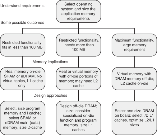
Memory design involves a number of considerations. The primary consideration is the application requirements: the operating system, the size, and the variability of the application processes. This largely determines the size of memory and how the memory will be addressed: real or virtual. Figure 4.1 is an outline for memory design, while Table 4.1 compares the relative area required for different memory technologies.
TABLE 4.1 Area Comparison for Different Memory Technologies
| Memory Technology | rbe | KB per Unit A |
| DRAM | 0.05–0.1 | 1800–3600 |
| SRAM | 0.6 | 300 |
| ROM/PROM | 0.2–0.8+ | 225–900 |
| eDRAM | 0.15 | 1200 |
| Flash: NAND | 0.02 | 10,000 |
Figure 4.1 An outline for memory design.
We start by looking at issues in SOC external and internal memories. We then examine scratchpad and cache memory to understand how they operate and how they are designed. After that, we consider the main memory problem, first the on-die memory and then the conventional dynamic RAM (DRAM) design. As part of the design of large memory systems, we look at multiple memory modules, interleaving, and memory system performance. Figure 4.2 presents the SOC memory design issues. In this chapter the interconnect, processors, and I/O are idealized so that the memory design trade-offs can be characterized.
Figure 4.2 The SOC memory model.

Table 4.2 shows the types of memory that can be integrated into an SOC design.
TABLE 4.2 Some Flash Memory (NAND) Package Formats (2- to 128-GB Size)

Example. Required functionality can play a big role in achieving performance. Consider the differences between the two paths of Figure 4.1: the maximum functionality path and the restricted functionality path. The difference seems slight, whether the memory is off-die or on-die. The resulting performance difference can be great because of the long off-die access time. If the memory (application data and program) can be contained in an on-die memory, the access time will be 3–10 cycles.
Off-die access times are an order of magnitude greater (30–100 cycles). To achieve the same performance, the off-die memory design must have an order of magnitude more cache, often split into multiple levels to meet access time requirements. Indeed, a cache bit can be 50 times larger than an on-die embedded DRAM (eDRAM) bit (see Chapter 2 and Section 4.13). So the true cost of the larger cache required for off-die memory support may be 10 by 50 or 500 DRAM bits. If a memory system uses 10K rbe for cache to support an on-die memory, the die would require 100K rbe to support off-die memory. That 90K rbe difference could possibly accommodate 450K eDRAM bits.
4.2 OVERVIEW
4.2.1 SOC External Memory: Flash
Flash technology is a rapidly developing technology with improvements announced regularly. Flash is not really a memory replacement but is probably better viewed as a disk replacement. However, in some circumstances and configurations, it can serve the dual purpose of memory and nonvolatile backup storage.
Flash memory consists of an array of floating gate transistors. These transistors are similar to MOS transistors but with a two-gate structure: a control gate and an insulated floating gate. Charge stored on the floating gate is trapped there, providing a nonvolatile storage. While the data can be rewritten, the current technology has a limited number of reliable rewrite cycles, usually less than a million. Since degradation with use can be a problem, error detection and correction are frequently implemented.
While the density is excellent for semiconductor devices, the write cycle limitation generally restricts the usage to storing infrequently modified data, such as programs and large files.
There are two types of flash implementations: NOR and NAND. The NOR implementation is more flexible, but the NAND provides a significantly better bit density. Hybrid NOR/NAND implementations are also possible with the NOR array acting as a buffer to the larger NAND array. Table 4.3 provides a comparison of these implementations.
TABLE 4.3 Comparison of Flash Memories
| Technology | NOR | NAND |
| Bit density (KB/A) | 1000 | 10,000 |
| Typical capacity | 64 MB | 16 GB (dice can be stacked by 4 or more) |
| Access time | 20–70 ns | 10 µs |
| Transfer rate (MB per sec.) | 150 | 300 |
| Write time(µs) | 300 | 200 |
| Addressability | Word or block | Block |
| Application | Program storage and limited data store | Disk replacement |
Flash memory cards come in various package formats; larger sizes are usually older (see Table 4.2). Small flash dice can be “stacked” with an SOC chip to present a single system/memory package. A flash die can also be stacked to create large (64–256 GB) single memory packages.
In current technology, flash usually is found in off-die implementations. However, there are a number of flash variants that are specifically designed to be compatible with ordinary SOC technology. SONOS [201] is a nonvolatile example, and Z-RAM [91] is a DRAM replacement example. Neither seems to suffer from rewrite cycle limitations. Z-RAM seems otherwise compatible with DRAM speeds while offering improved density. SONOS offers density but with slower access time than eDRAM.
4.2.2 SOC Internal Memory: Placement
The most important and obvious factor in memory system design is the placement of the main memory: on-die (the same die as the processor) or off-die (on its own die or on a module with multiple dice). As pointed out in Chapter 1, this factor distinguishes conventional workstation processors and application-oriented board designs from SOC designs.
The design of the memory system is limited by two basic parameters that determine memory systems performance. The first is the access time. This is the time for a processor request to be transmitted to the memory system, access a datum, and return it back to the processor. Access time is largely a function of the physical parameters of the memory system—the physical distance between the processor and the memory system, or the bus delay, the chip delay, and so on. The second parameter is memory bandwidth, the ability of the memory to respond to requests per unit time. Bandwidth is primarily determined by the way the physical memory system is organized—the number of independent memory arrays and the use of special sequential accessing modes.
The cache system must compensate for limits on memory access time and bandwidth.
The workstation processor, targeting high performance, requires a very efficient memory system, a task made difficult by memory placement off-die. Table 4.4 compares the memory system design environments.
TABLE 4.4 Comparing System Design Environments
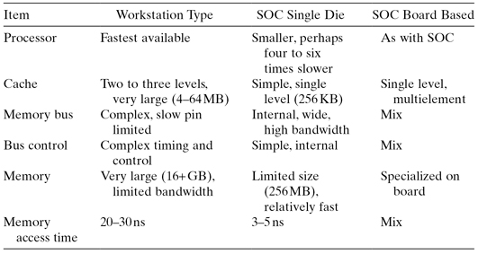
The workstation and board-based memory design is clearly a greater challenge for designers. Special attention must be paid to the cache, which must make up for the memory placement difficulties.
4.2.3 The Size of Memory
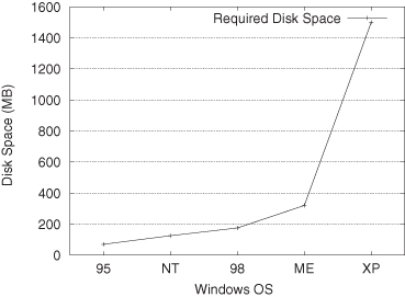
As it will become obvious in this chapter, designing for large off-die memory is the key problem in system board designs. So why not limit memory to sizes that could be incorporated on a die? In a virtual memory system, we can still access large address spaces for applications. For workstations, the application environment (represented by the operating system) has grown considerably (see Figure 4.3). As the environment continues to grow, so too does the working set or the active pages of storage. This requires more real (physical) memory to hold a sufficient number of pages to avoid excessive page swapping, which can destroy performance. Board-based systems face a slightly different problem. Here, the media-based data sets are naturally very large and require large bandwidths from memory and substantial processing ability from the media processor. Board-based systems have an advantage, however, as the access time is rarely a problem so long as the bandwidth requirements are met. How much memory can we put on a die? Well, that depends on the technology (feature size) and the required performance. Table 4.1 shows the area occupied for various technologies. The eDRAM size assumes a relatively large memory array (see later in this chapter). So, for example, in a 45-nm technology, we might expect to have about 49.2 kA/cm2 or about 8 MB of eDRAM. Advancing circuit design and technology could significantly improve that, but it does seem that about 64 MB would be a limit, unless a compatible flash technology becomes available.
Figure 4.3 Required disk space for several generations of Microsoft’s Windows operating system. The newer Vista operating system requires 6 GB.
4.3 SCRATCHPADS AND CACHE MEMORY
Smaller memories are almost always faster than larger memory, so it is useful to keep frequently used (or anticipated) instructions and data in a small, easily accessible (one cycle access) memory. If this memory is managed directly by the programmer, it is called a scratchpad memory; if it is managed by the hardware, it is called a cache.
Since management is a cumbersome process, most general-purpose computers use only cache memory. SOC, however, offers the potential of having the scratchpad alternative. Assuming that the application is well-known, the programmer can explicitly control data transfers in anticipation of use. Eliminating the cache control hardware offers additional area for larger scratchpad size, again improving performance.
SOC implements scratchpads usually for data and not for instructions, as simple caches work well for instructions. Furthermore, it is not worth the programming effort to directly manage instruction transfers.
The rest of this section treats the theory and experience of cache memory. Because there has been so much written about cache, it is easy to forget the simpler and older scratchpad approach, but with SOC, sometimes the simple approach is best.
Caches work on the basis of the locality of program behavior [113]. There are three principles involved:
1. Spatial Locality. Given an access to a particular location in memory, there is a high probability that other accesses will be made to either that or neighboring locations within the lifetime of the program.
2. Temporal Locality. Given a sequence of references to n locations, there will be references into the same locations with high probability.
3. Sequentiality. Given that a reference has been made to location s, it is likely that within the next few references, there will be a reference to the location of s + 1. This is a special case of spatial locality.
The cache designer must deal with the processor’s accessing requirements on the one hand, and the memory system’s requirements on the other. Effective cache designs balance these within cost constraints.
4.4 BASIC NOTIONS
Processor references contained in the cache are called cache hits. References not found in the cache are called cache misses. On a cache miss, the cache fetches the missing data from memory and places it in the cache. Usually, the cache fetches an associated region of memory called the line. The line consists of one or more physical words accessed from a higher-level cache or main memory. The physical word is the basic unit of access to the memory.
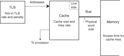
The processor–cache interface has a number of parameters. Those that directly affect processor performance (Figure 4.4) include the following:
1. Physical word—unit of transfer between processor and cache.
Typical physical word sizes:
2–4 bytes—minimum, used in small core-type processors
8 bytes and larger—multiple instruction issue processors (superscalar)
2. Block size (sometimes called line)—usually the basic unit of transfer between cache and memory. It consists of n physical words transferred from the main memory via the bus.
3. Access time for a cache hit—this is a property of the cache size and organization.
4. Access time for a cache miss—property of the memory and bus.
5. Time to compute a real address given a virtual address (not-in-translation lookaside buffer [TLB] time)—property of the address translation facility.
6. Number of processor requests per cycle.
Figure 4.4 Parameters affecting processor performance.
Cache performance is measured by the miss rate or the probability that a reference made to the cache is not found. The miss rate times the miss time is the delay penalty due to the cache miss. In simple processors, the processor stalls on a cache miss.
IS CACHE A PART OF THE PROCESSOR?
For many IP designs, the first-level cache is integrated into the processor design, so what and why do we need to know cache details? The most obvious answer is that an SOC consists of multiple processors that must share memory, usually through a second-level cache. Moreover, the details of the first-level cache may be essential in achieving memory consistency and proper program operation. So for our purpose, the cache is a separate, important piece of the SOC. We design the SOC memory hierarchy, not an isolated cache.
4.5 CACHE ORGANIZATION
A cache uses either a fetch-on-demand or a prefetch strategy. The former organization is widely used with simple processors. A demand fetch cache brings a new memory locality into the cache only when a miss occurs. The prefetch cache attempts to anticipate the locality about to be requested and prefetches it. It is commonly used in I-caches.
There are three basic types of cache organization: fully associative (FA) mapping (Figure 4.5), direct mapping (Figure 4.6), and set associative mapping (Figure 4.7, which is really a combination of the other two). In an FA cache, when a request is made, the address is compared (COMP) to the addresses of all entries in the directory. If the requested address is found (a directory hit), the corresponding location in the cache is fetched; otherwise, a miss occurs.
Figure 4.5 Fully associative mapping.

Figure 4.6 Direct mapping.

Figure 4.7 Set associative (multiple direct-mapped caches) mapping.

In a direct-mapped cache, the lower-order line address bits access the directory (index bits in Figure 4.8). Since multiple line addresses map into the same location in the cache directory, the upper line address bits (tag bits) must be compared to the directory address to validate a hit. If a comparison is not valid, the result is a miss. The advantage of the direct-mapped cache is that a reference to the cache array itself can be made simultaneously with the access to the directory.
Figure 4.8 Address partitioned by cache usage.

The address given to the cache by the processor is divided into several pieces, each of which has a different role in accessing data. In an address partitioned as in Figure 4.8, the most significant bits that are used for comparison (with the upper portion of a line address contained in the directory) are called the tag.
The next field is called the index, and it contains the bits used to address a line in the cache directory. The tag plus the index is the line address in memory.
The next field is the offset, and it is the address of a physical word within a line.
Finally, the least significant address field specifies a byte in a word. These bits are not usually used by the cache since the cache references a word. (An exception arises in the case of a write that modifies only a part of a word.)
The set associative cache is similar to the direct-mapped cache. Bits from the line address are used to address a cache directory. However, now there are multiple choices: Two, four, or more complete line addresses may be present in the directory. Each address corresponds to a location in a subcache. The collection of these subcaches forms the total cache array. These subarrays can be accessed simultaneously, together with the cache directory. If any of the entries in the cache directory match the reference address, then there is a hit, and the matched subcache array is sent back to the processor. While selection in the matching process increases the cache access time, the set associative cache access time is usually better than that of the fully associative mapped cache. But the direct-mapped cache provides the fastest processor access to cache data for any given cache size.
4.6 CACHE DATA
Cache size largely determines cache performance (miss rate). The larger the cache, the lower the miss rate. Almost all cache miss rate data are empirical and, as such, have certain limitations. Cache data are strongly program dependent. Also, data are frequently based upon older machines, where the memory and program size were fixed and small. Such data show low miss rate for relatively small size caches. Thus, there is a tendency for the measured miss rate of a particular cache size to increase over time. This is simply the result of measurements made on programs of increasing size. Some time ago, Smith [224] developed a series of design target miss rates (DTMRs) that represent an estimate of what a designer could expect from an integrated (instruction and data) cache. These data are presented in Figure 4.9 and give an idea of typical miss rates as a function of cache and line sizes.
Figure 4.9 A design target miss rate per reference to memory (fully associative, demand fetch, fetch [allocate] on write, copy-back with LRU replacement) [223, 224].

For cache sizes larger than 1 MB, a general rule is that doubling the size halves the miss rate. The general rule is less valid in transaction-based programs.
4.7 WRITE POLICIES
How is memory updated on a write? One could write to both cache and memory (write-through or WT), or write only to the cache (copy-back or CB—sometimes called write-back), updating memory when the line is replaced. These two strategies are the basic cache write policies (Figure 4.10).
Figure 4.10 Write policies: (a) write-through cache (no allocate on write) and (b) copy-back cache (allocate on write).

The write-through cache (Figure 4.10a) stores into both cache and main memory on each CPU store.
Advantage: This retains a consistent (up-to-date) image of program activity in memory.
Disadvantage: Memory bandwidth may be high—dominated by write traffic.
In the copy-back cache (Figure 4.10b), the new data are written to memory when the line is replaced. This requires keeping track of modified (or “dirty”) lines, but results in reduced memory traffic for writes:
1. Dirty bit is set if a write occurs anywhere in line.
2. From various traces [223], the probability that a line to be replaced is dirty is 47% on average (ranging from 22% to 80%).
3. Rule of thumb: Half of the data lines replaced are dirty. So, for a data cache, assume 50% are dirty lines, and for an integrated cache, assume 30% are dirty lines.
Most larger caches use copy-back; write-through is usually restricted to either small caches or special-purpose caches that provide an up-to-date image of memory. Finally, what should we do when a write (or store) instruction misses in the cache? We can fetch that line from memory (write allocate or WA) or just write into memory (no write allocate or NWA). Most write-through caches do not allocate on writes (WTNWA) and most copy back caches do allocate (CBWA).
4.8 STRATEGIES FOR LINE REPLACEMENT AT MISS TIME
What happens on a cache miss? If the reference address is not found in the directory, a cache miss occurs. Two actions must promptly be taken: (1) The missed line must be fetched from the main memory, and (2) one of the current cache lines must be designated for replacement by the currently accessed line (the missed line).
4.8.1 Fetching a Line
In a write-through cache, fetching a line involves accessing the missed line and the replaced line is discarded (written over).
For a copy-back policy, we first determine whether the line to be replaced is dirty (has been written to) or not. If the line is clean, the situation is the same as with the write-through cache. However, if the line is dirty, we must write the replaced line back to memory.
In accessing a line, the fastest approach is the nonblocking cache or the prefetching cache. This approach is applicable in both write-through and copy-back caches. Here, the cache has additional control hardware to allow the cache miss to be handled (or bypassed), while the processor continues to execute. This strategy only works when the miss is accessing cache data that are not currently required by the processor. Nonblocking caches perform best with compilers that provide prefetching of lines in anticipation of processor use. The effectiveness of nonblocking caches depends on
1. the number of misses that can be bypassed while the processor continues to execute; and
2. the effectiveness of the prefetch and the adequateness of the buffers to hold the prefetch information; the longer the prefetch is made before expected use, the less the miss delay, but this also means that the buffers or registers are occupied and hence are not available for (possible) current use.
4.8.2 Line Replacement
The replacement policy selects a line for replacement when the cache is full. There are three replacement policies that are widely used:
1. Least Recently Used (LRU). The line that was least recently accessed (by a read or write) is replaced.
2. First In–First Out (FIFO). The line that had been in the cache the longest is replaced.
3. Random Replacement (RAND). Replacement is determined randomly.
Since the LRU policy corresponds to the concept of temporal locality, it is generally the preferred policy. It is also the most complex to implement. Each line has a counter that is updated on a read (or write). Since these counters could be large, it is common to create an approximation to the true LRU with smaller counters.
While LRU performs better than either FIFO or RAND, the use of the simpler RAND or FIFO only amplifies the LRU miss rate (DTMR) by about 1.10 (i.e., 10%) [223].
4.8.3 Cache Environment: Effects of System, Transactions, and Multiprogramming
Most available cache data are based upon trace studies of user applications. Actual applications are run in the context of the system. The operating system tends to slightly increase (20% or so) the miss rate experienced by a user program [7].
Multiprogramming environments create special demands on a cache. In such environments, the cache miss rates may not be affected by increasing cache size. There are two environments:
1. A Multiprogrammed Environment. The system, together with several programs, is resident in memory. Control is passed from program to program after a number of instructions, Q, have been executed, and eventually returns to the first program. This kind of environment results in what is called a warm cache. When a process returns for continuing execution, it finds some, but not all, of its most recently used lines in the cache, increasing the expected miss rate (Figure 4.11 illustrates the effect).
2. Transaction Processing. While the system is resident in memory together with a number of support programs, short applications (transactions) run through to completion. Each application consists of Q instructions. This kind of environment is sometimes called a cold cache. Figure 4.12 illustrates the situation.
Figure 4.11 Warm cache: cache miss rates for a multiprogrammed environment switching processes after Q instructions.

Figure 4.12 Cold cache: cache miss rates for a transaction environment switching processes after Q instructions.

Both of the preceding environments are characterized by passing control from one program to another before completely loading the working set of the program. This can significantly increase the miss rate.
4.9 OTHER TYPES OF CACHE
So far, we have considered only the simple integrated cache (also called a “unified” cache), which contains both data and instructions. In the next few sections, we consider various other types of cache. The list we present (Table 4.5) is hardly exhaustive, but it illustrates some of the variety of cache designs possible for special or even commonplace applications.
TABLE 4.5 Common Types of Cache
| Type | Where It Is Usually Used |
| Integrated (or unified) | The basic cache that accommodates all references (I and D). This is commonly used as the second- and higher-level cache. |
| Split caches I and D | Provides additional cache access bandwidth with some increase in the miss rate (MR). Commonly used as a first-level processor cache. |
| Sectored cache | Improves area effectiveness (MR for given area) for on-chip cache. |
| Multilevel cache | The first level has fast access; the second level is usually much larger than the first to reduce time delay in a first-level miss. |
| Write assembly cache | Specialized, reduces write traffic, usually used with a WT on-chip first-level cache. |
Most currently available microprocessors use split I- and D-caches, described in the next section.
4.10 SPLIT I- AND D-CACHES AND THE EFFECT OF CODE DENSITY
Multiple caches can be incorporated into a single processor design, each cache serving a designated process or use. Over the years, special caches for systems code and user code or even special input/output (I/O) caches have been considered. The most popular configuration of partitioned caches is the use of separate caches for instructions and data.
Separate instruction and data caches provide significantly increased cache bandwidth, doubling the access capability of the cache ensemble. I- and D-caches come at some expense, however; a unified cache with the same size as the sum of a data and instruction cache has a lower miss rate. In the unified cache, the ratio of instruction to data working set elements changes during the execution of the program and is adapted to by the replacement strategy.
Split caches have implementation advantages. Since the caches need not be split equally, a 75–25% or other split may prove more effective. Also, the I-cache is simpler as it is not required to handle stores.
4.11 MULTILEVEL CACHES
4.11.1 Limits on Cache Array Size
The cache consists of a static RAM (SRAM) array of storage cells. As the array increases in size, so does the length of the wires required to access its most remote cell. This translates into the cache access delay, which is a function of the cache size, organization, and the process technology (feature size, f). McFarland [166] has modeled the delay and found that an approximation can be represented as
![]()
where f is the feature size in microns, C is the cache array capacity in kilobyte, and A is the degree of associativity (where direct map = 1).
The effect of this equation (for A = 1) can be seen in Figure 4.13. If we limit the level 1 access time to under 1 ns, we are probably limited to a cache array of about 32 KB. While it is possible to interleave multiple arrays, the interleaving itself has an overhead. So usually, L1 caches are less than 64 KB; L2 caches are usually less than 512 KB (probably interleaved using smaller arrays); and L3 caches use multiple arrays of 256 KB or more to create large caches, often limited by die size.
Figure 4.13 Cache access time (for a single array) as a function of cache array size.

4.11.2 Evaluating Multilevel Caches
In the case of a multilevel cache, we can evaluate the performance of both levels using L1 cache data. A two-level cache system is termed inclusive if all the contents of the lower-level cache (L1) are also contained in the higher-level cache (L2).
Second-level cache analysis is achieved using the principle of inclusion; that is, a large, second-level cache includes the same lines as in the first-level cache. Thus, for the purpose of evaluating performance, we can assume that the first-level cache does not exist. The total number of misses that occur in a second-level cache can be determined by assuming that the processor made all of its requests to the second-level cache without the intermediary first-level cache.
There are design considerations in accommodating a second-level cache to an existing first-level cache. The line size of the second-level cache should be the same as or larger than the first-level cache. Otherwise, if the line size in the second-level cache were smaller, loading the line in the first-level cache would simply cause two misses in the second-level cache. Further, the second-level cache should be significantly larger than the first-level; otherwise, it would have no benefit.
In a two-level system, as shown in Figure 4.14, with first-level cache, L1, and second-level cache, L2, we define the following miss rates [202]:
1. A local miss rate is simply the number of misses experienced by the cache divided by the number of references to it. This is the usual understanding of miss rate.
2. The global miss rate is the number of L2 misses divided by the number of references made by the processor. This is our primary measure of the L2 cache.
3. The solo miss rate is the miss rate the L2 cache would have if it were the only cache in the system. This is the miss rate defined by the principle of inclusion. If L2 contains all of L1, then we can find the number of L2 misses and the processor reference rate, ignoring the presence of the L1 cache. The principle of inclusion specifies that the global miss rate is the same as the solo miss rate, allowing us to use the solo miss rate to evaluate a design.
Figure 4.14 A two-level cache.
The preceding data (read misses only) illustrate some salient points in multilevel cache analysis and design:
1. So long as the L1 cache is the same as or larger than the L2 cache, analysis by the principle of inclusion provides a good estimate of the behavior of the L2 cache.
2. When the L2 cache is significantly larger than the L1 cache, it can be considered independent of the L1 parameters. Its miss rate corresponds to a solo miss rate.
EXAMPLE 4.1

Miss penalties:
| Miss in L1, hit in L2: | 2 cycles |
| Miss in L1, miss in L2: | 15 cycles |
Suppose we have a two-level cache with miss rates of 4% (L1) and 1% (L2). Suppose the miss in L1 and the hit in L2 penalty is 2 cycles, and the miss penalty in both caches is 15 cycles (13 cycles more than a hit in L2). If a processor makes one reference per instruction, we can compute the excess cycles per instruction (CPIs) due to cache misses as follows:


Note: the L2 miss penalty is 13 cycles, not 15 cycles, since the 1% L2 misses have already been “charged” 2 cycles in the excess L1 CPI:

The cache configurations for some recent SOCs are shown in Table 4.6.
TABLE 4.6 SOC Cache Organization
| SOC | L1 Cache | L2 Cache |
| NetSilicon NS9775 [185] | 8-KB I-cache, 4-KB D-cache | — |
| NXP LH7A404 [186] | 8-KB I-cache, 8-KB D-cache | — |
| Freescale e600 [101] | 32-KB I-cache, 32-KB D-cache | 1 MB with ECC |
| Freescale PowerQUICC III [102] | 32-KB I-cache, 32-KB D-cache | 256 KB with ECC |
| ARM1136J(F)-S [24] | 64-KB I-cache, 64-KB D-cache | Max 512 KB |
4.11.3 Logical Inclusion
True or logical inclusion, where all the contents of L1 reside also in L2, should not be confused with statistical inclusion, where usually, L2 contains the L1 data. There are a number of requirements for logical inclusion. Clearly, the L1 cache must be write-through; the L2 cache need not be. If L1 were copy-back, then a write to a line in L1 would not go immediately to L2, so L1 and L2 would differ in contents.
When logical inclusion is required, it is probably necessary to actively force the contents to be the same and to use consistent cache policies.
Logical inclusion is a primary concern in shared memory multiprocessor systems that require a consistent memory image.
4.12 VIRTUAL-TO-REAL TRANSLATION
The TLB provides the real addresses used by the cache by translating the virtual addresses into real addresses.
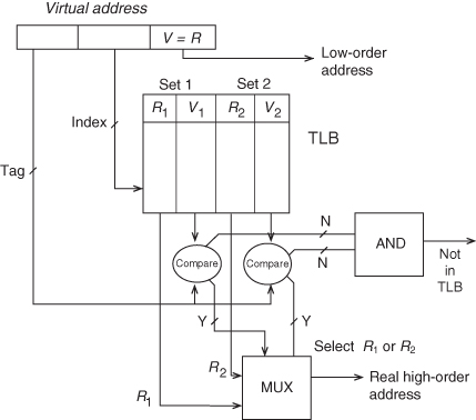
Figure 4.15 shows a two-way set associative TLB. The page address (the upper bits of the virtual address) is composed of the bits that require translation. Selected virtual address bits address the TLB entries. These are selected (or hashed) from the bits of the virtual address. This avoids too many address collisions, as might occur when both address and data pages have the same, say, “000,” low-order page addresses. The size of the virtual address index is equal to log2 t, where t is the number of entries in the TLB divided by the degree of set associativity. When a TLB entry is accessed, a virtual and real translation pair from each entry is accessed. The virtual addresses are compared to the virtual address tag (the virtual address bits that were not used in the index). If a match is found, the corresponding real address is multiplexed to the output of the TLB.
Figure 4.15 TLB with two-way set associativity.
With careful assignment of page addresses, the TLB access can occur at the same time as the cache access. When a translation is not found in the TLB, the process described in Chapter 1 must be repeated to create a correct virtual-to-real address pair in the TLB. This may require more than 10 cycles; TLB misses—called not-in-TLB—are costly to performance. TLB access in many ways resembles cache access. FA organization of TLB is generally slow, but four-way or higher set associative TLBs perform well and are generally preferred.
Typical TLB miss rates are shown in Figure 4.16. FA data are similar to four-way set associative.
Figure 4.16 Not-in-TLB rate.

For those SOC or board-based systems that use virtual addressing, there are additional considerations:
1. Small TLBs may create excess not-in-TLB faults, adding time to program execution.
2. If the cache uses real addresses, the TLB access must occur before the cache access, increasing the cache access time.
Excess not-in-TLB translations can generally be controlled through the use of a well-designed TLB. The size and organization of the TLB depends on performance targets.
Typically, separate instruction and data TLBs are used. Both TLBs might use 128-entry, two-way set associative, and might use LRU replacement algorithm. The TLB conflagrations of some recent SOCs are shown in Table 4.7.
TABLE 4.7 SOC TLB Organization
| SOC | Organization | Number of Entries |
| Freescale e600 [101] | Separate I-TLB, D-TLB | 128-entry, two-way set associative, LRU |
| NXP LH7A404 [186] | Separate I-TLB, D-TLB | 64-entry each |
| NetSilicon NS9775 (ARM926EJ-S) [185] | Mixed | 32-entry two-way set associative |
4.13 SOC (ON-DIE) MEMORY SYSTEMS
On-die memory design is a special case of the general memory system design problem, considered in the next section. The designer has much greater flexibility in the selection of the memory itself and the overall cache-memory organization. Since the application is known, the general size of both the program and data store can be estimated. Frequently, part of the program store is designed as a fixed ROM. The remainder of memory is realized with either SRAM or DRAM. While the SRAM is realized in the same process technology as the processor, usually DRAM is not. An SRAM bit consists of a six-transistor cell, while the DRAM uses only one transistor plus a deep trench capacitor. The DRAM cell is designed for density; it uses few wiring layers. DRAM design targets low refresh rates and hence low leakage currents. A DRAM cell uses a nonminimum length transistor with a higher threshold voltage, (VT), to provide a lower-leakage current. This leads to lower gate overdrive and slower switching. For a stand-alone die, the result is that the SRAM is 10–20 times faster and 10 or more times less dense than DRAM.
eDRAM [33, 125] has been introduced as a compromise for use as an on-die memory. Since there are additional process steps in realizing an SOC with eDRAM, the macro to generate the eDRAM is fabrication specific and is regarded as a hard (or at least firm) IP. The eDRAM has an overhead (Figure 4.17) resulting in less density than DRAM. Process complexity for the eDRAM can include generating three additional mask layers resulting in 20% additional cost than that for the DRAM.
Figure 4.17 On-die SRAM and DRAM. The eDRAM must accommodate the process requirements of the logic, representing an overhead. SRAM is unaffected.

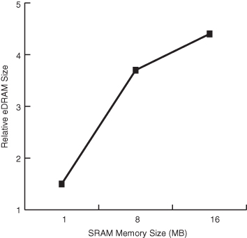
An SOC, using the eDRAM approach, integrates high-speed, high-leakage logic transistors with lower-speed, lower-leakage memory transistors on the same die. The advantage for eDRAM lies in its density as shown in Figure 4.18. Therefore, one key factor for selecting eDRAM over SRAM is the size of the memory required.
Figure 4.18 The relative density advantage eDRAM improves with memory size.
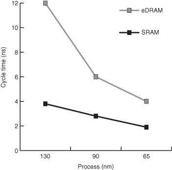
Having paid the process costs for eDRAM, the timing parameters for eDRAM are much better than conventional DRAM. The cycle time (and access time) is much closer to SRAM, as shown in Figure 4.19. All types of on-die memory enjoy the advantage of bandwidth as a whole memory column can be accessed at each cycle.
Figure 4.19 Cycle time for random memory accesses.
A final consideration in memory selection is the projected error rate due to radiation (called the soft error rate or SER). Each DRAM cell stores significantly larger amounts of charge than in the SRAM cell. The SRAM cells are faster and easier to flip, with correspondingly higher SER. Additionally, for an SRAM cell, as technology scales, the critical amount of charge for determining an error decreases due to scaling of supply voltages and cell capacitances. The differences are shown in Figure 4.20. At even 130-nm feature size, the SER for SRAM is about 1800 times higher than for eDRAM. Of course, more error-prone SRAM implementation can compensate by a more extensive use of error-correcting codes (ECCs), but this comes with its own cost.
Figure 4.20 The ratio of soft error rates of SRAM to eDRAM.

Ultimately, the selection of on-die memory technology depends on fabrication process access and memory size required.
4.14 BOARD-BASED (OFF-DIE) MEMORY SYSTEMS
In many processor design situations (probably all but the SOC case), the main memory system is the principal design challenge.
As processor ensembles can be quite complex, the memory system that serves these processors is correspondingly complex.
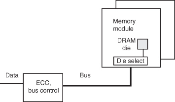
The memory module consists of all the memory chips needed to forward a cache line to the processor via the bus. The cache line is transmitted as a burst of bus word transfers. Each memory module has two important parameters: module access time and module cycle time. The module access time is simply the amount of time required to retrieve a word into the output memory buffer register of a particular memory module, given a valid address in its address register. Memory service (or cycle) time is the minimum time between requests directed at the same module. Various technologies present a significant range of relationships between the access time and the service time. The access time is the total time for the processor to access a line in memory. In a small, simple memory system, this may be little more than chip access time plus some multiplexing and transit delays. The service time is approximately the same as the chip cycle time. In a large, multimodule memory system (Figure 4.21), the access time may be greatly increased, as it now includes the module access time plus transit time, bus accessing overhead, error detection, and correction delay.
Figure 4.21 Accessing delay in a complex memory system. Access time includes chip accessing, module overhead, and bus transit.
After years of rather static evolution of DRAM memory chips, recent years have brought about significant new emphasis on the performance (rather than simply the size) of memory chips.
The first major improvement to DRAM technology is synchronous DRAM (SDRAM). This approach synchronizes the DRAM access and cycle time to the bus cycle. Additional enhancements accelerate the data transfer and improves the electrical characteristics of the bus and module. There are now multiple types of SDRAM. The basic DRAM types are the following:
1. DRAM. Asynchronous DRAM.
2. SDRAM. The memory module timing is synchronized to the memory bus clock.
3. Double data rate (DDR) SDRAM. The memory module fetches a double-sized transfer unit for each bus cycle and transmits at twice the bus clock rate.
In the next section, we present the basics of the (asynchronous) DRAM, following that of the more advanced SDRAMs.
4.15 SIMPLE DRAM AND THE MEMORY ARRAY
The simplest asynchronous DRAM consists of a single memory array with 1 (and sometimes 4 or 16) output bits. Internal to the chip is a two-dimensional array of memory cells consisting of rows and columns. Thus, half of the memory address is used to specify a row address, one of 2n/2 row lines, and the other half of the address is similarly used to specify one of 2n/2 column lines (Figure 4.22). The cell itself that holds the data is quite simple, consisting merely of a MOS transistor holding a charge (a capacitance). As this discharges over time, it must continually be refreshed, once every several milliseconds.
Figure 4.22 A memory chip.

With large-sized memories, the number of address lines dominates the pinout of the chip. In order to conserve these pins and to provide a smaller package for better overall density, the row and column addresses are multiplexed onto the same lines (input pins) for entry onto the chip. Two additional lines are important here: row address strobe (RAS) and column address strobe (CAS). These gate first the row address, then the column address into the chip. The row and column addresses are then decoded to select one out of the 2n/2 possible lines. The intersection of the active row and column lines is the desired bit of information. The column line’s signals are then amplified by a sense amplifier and are transmitted to the output pin (data out, or Dout) during a read cycle. During a write cycle, the write-enable (WE) signal stores the data-in (Din) signal to specify the contents of the selected bit address.
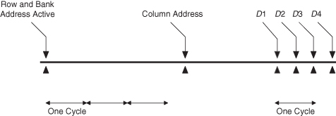
All of these actions happen in a sequence approximated in the timing diagram in Figure 4.23. At the beginning of a read from memory, the RAS line is activated. With the RAS active and the CAS inactive, the information on the address lines is interpreted as the row address and is stored into the row address register. This activates the row decoder and the selected row line in the memory array. The CAS is then activated, which gates the column address lines into a column address register. Note that
1. the two rise times on CAS represent the earliest and latest that this signal may rise with respect to the column address signals and
2. WE is inactive during read operations.
Figure 4.23 Asynchronous DRAM chip timing.

The column address decoder then selects a column line; at the intersection of the row and column line is the desired data bit. During a read cycle, the WE is inactive (low) and the output line (Dout) is at a high-impedance state until it is activated either high or low depending on the contents of the selected memory cell.
The time from the beginning of RAS until the data output line is activated is a very important parameter in the memory module design. This is called the chip access time or tchip access. The other important chip timing parameter is the cycle time of the memory chip (tchip cycle). This is not the same as the access time, as the selected row and column lines must recover before the next address can be entered and the read process repeated.
The asynchronous DRAM module does not simply consist of memory chips (Figure 4.24). In a memory system with p bits per physical word, and 2n words in a module, the n address bits enter the module and are usually directed at a dynamic memory controller chip. This chip, in conjunction with a memory timing controller, provides the following functions:
1. multiplexing the n address bits into a row and a column address for use by the memory chips,
2. the creation of the correct RAS and CAS signal lines at the appropriate time, and
3. providing a timely refresh of the memory system.
Figure 4.24 An asynchronous DRAM memory module.
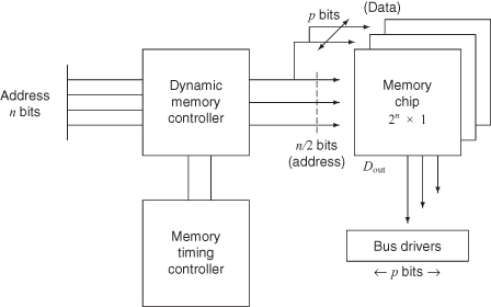
Since the dynamic memory controller output drives all p bits, and hence p chips, of the physical word, the controller output may also require buffering. As the memory read operation is completed, the data-out signals are directed at bus drivers, which then interface to the memory bus, which is the interface for all of the memory modules.
Two features found on DRAM chips affect the design of the memory system. These “burst” mode-type features are called
1. nibble mode and
2. page mode.
Both of these are techniques for improving the transfer rate of memory words. In nibble mode, a single address (row and column) is presented to the memory chip and the CAS line is toggled repeatedly. Internally, the chip interprets this CAS toggling as a mod 2w progression of low-order column addresses. Thus, sequential words can be accessed at a higher rate from the memory chip. For example, for w = 2, we could access four consecutive low-order bit addresses, for example:
![]()
and then return to the original bit address.
In page mode, a single row is selected and nonsequential column addresses may be entered at a high rate by repeatedly activating the CAS line (similar to nibble mode, Figure 4.23). Usually, this is used to fill a cache line.
While terminology varies, the nibble mode usually refers to the access of (up to) four consecutive words (a nibble) starting on a quad word address boundary. Table 4.8 illustrates some SOC memory size, position and type. The newer DDR SDRAM and follow ons are discussed in the next section.
TABLE 4.8 SOC Memory Designs

4.15.1 SDRAM and DDR SDRAM
The first major improvement to the DRAM technology is the SDRAM. This approach, as mentioned before, synchronizes the DRAM access and cycle to the bus cycle. This has a number of significant advantages. It eliminates the need for separate memory clocking chips to produce the RAS and CAS signals. The rising edge of the bus clock provides the synchronization. Also, by extending the package to accommodate multiple output pins, versions that have 4, 8, and 16 pins allow more modularity in memory sizing.
With the focus on the bus and memory bus interface, we further improve bus bandwidth by using differential data and address lines. Now when the clock line rises, the complement clock falls, but midway through the cycle, the clock line falls and the complement clock rises. This affords the possibility to transmit synchronous data twice during each cycle: once on the rising edge of the clock signal and once on the rising edge of the complement clock. By using this, we are able to double the data rate transmitted on the bus. The resulting memory chips are called DDR SDRAMs (Figure 4.25). Also, instead of selecting a row and a column for each memory reference, it is possible to select a row and leave it selected (active) while multiple column references are made to the same row (Figure 4.26).
Figure 4.25 Internal configuration of DDR SDRAM.

Figure 4.26 A line fetch in DDR SDRAM.
In cases where spatial locality permits, the read and write times are improved by eliminating the row select delay. Of course, when a new row is referenced, then the row activation time must be added to the access time. Another improvement introduced in SDRAMs is the use of multiple DRAM arrays, usually either four or eight. Depending on the chip implementation, these multiple arrays can be independently accessed or sequentially accessed, as programmed by the user. In the former case, each array can have an independently activated row providing an interleaved access to multiple column addresses. If the arrays are sequentially accessed, then the corresponding rows in each array are activated and longer bursts of consecutive data can be supported. This is particularly valuable for graphics applications.
The improved timing parameters of the modern memory chip results from careful attention to the electrical characteristic of the bus and the chip. In addition to the use of differential signaling (initially for data, now for all signals), the bus is designed to be a terminated strip transmission line. With the DDR3 (closely related to graphics double data rate [GDDR3]), the termination is on-die (rather than simply at the end of the bus), and special calibration techniques are used to ensure accurate termination.
The DDR chips that support interleaved row accesses with independent arrays must carry out a 2n data fetch from the array to support the DDR. So, a chip with four data out (n = 4) lines must have arrays that fetch 8 bits. The DDR2 arrays typically fetch 4n, so with n = 4, the array would fetch 16 bits. This enables higher data transmission rates as the array is accessed only once for every four-bus half-cycles.
Some typical parameters are shown in Tables 4.9 and 4.10. While representatives of all of these DRAMs are in production at the time of writing, the asynchronous DRAM and the SDRAM are legacy parts and are generally not used for new development. The DDR3 part was introduced for graphic application configurations. For most cases, the parameters are typical and for common configurations. For example, the asynchronous DRAM is available with 1, 4, and 16 output pins. The DDR SDRAMs are available with 4, 8, and 16 output pins. Many other arrangements are possible.
TABLE 4.9 Configuration Parameters for Some Typical DRAM Chips Used in a 64-bit Module
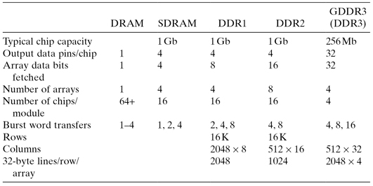
TABLE 4.10 Timing Parameters for Some Typical DRAM Modules (64 bits)

Multiple (up to four) DDR2 SDRAMs can be configured to share a common bus (Figure 4.27). In this case, when a chip is “active” (i.e., it has an active row), the on-die termination is unused. When there are no active rows on the die, the termination is used. Typical server configurations then might have four modules sharing a bus (called a channel) and a memory controller managing up to two buses (see Figure 4.27). The limit of two is caused simply by the large number of tuned strip and microstrip transmission lines that must connect the controller to the buses. More advanced techniques place a channel buffer between the module and a very high-speed channel. This advanced channel has a smaller width (e.g., 1 byte) but a much higher data rate (e.g., 8×). The net effect leaves the bandwidth per module the same, but now the number of wires entering the controller has decreased, enabling the controller to manage more channels (e.g., 8).
Figure 4.27 SDRAM channels and controller.

4.15.2 Memory Buffers
The processor can sustain only a limited number of outstanding memory references before it suspends processing and the generation of further memory references. This can happen either as a result of logical dependencies in the program or because of an insufficient buffering capability for outstanding requests. The significance of this is that the achievable memory bandwidth is decreased as a consequence of the pause in the processing, for the memory can service only as many requests as are made by the processor.
Examples of logical dependencies include branches and address interlocks. The program must suspend computation until an item has been retrieved from memory.
Associated with each outstanding memory request is certain information that specifies the nature of the request (e.g., a read or a write operation), the address of the memory location, and sufficient information to route requested data back to the requestor. All this information must be buffered either in the processor or in the memory system until the memory reference is complete. When the buffer is full, further requests cannot be accepted, requiring the processor be stalled.
In interleaved memory, the modules usually are not all equally congested. So, it is useful to maximize the number of requests made by the processor, in the hope that the additional references will be to relatively idle modules and will lead to a net increase in the achieved bandwidth. If maximizing the bandwidth of memory is a primary objective, we need buffering of memory requests up to the point at which the logical dependencies in the program become the limiting factor.
4.16 MODELS OF SIMPLE PROCESSOR–MEMORY INTERACTION
In systems with multiple processors or with complex single processors, requests may congest the memory system. Either multiple requests may occur at the same time, providing bus or network congestion, or requests arising from different sources may request access to the memory system. Requests that cannot be immediately honored by the memory system result in memory systems contention. This contention degrades the bandwidth and is possible to achieve from the memory system.
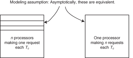
In the simplest possible arrangement, a single simple processor makes a request to a single memory module. The processor ceases activity (as with a blocking cache) and waits for service from the module. When the module responds, the processor resumes activity. Under such an arrangement, the results are completely predictable. There can be no contention of the memory system since only one request is made at a time to the memory module. Now suppose we arrange to have n simple processors access m independent modules. Contention develops when multiple processors access the same module. Contention results in a reduced average bandwidth available to each of the processors. Asymptotically, a processor with a nonblocking cache making n requests to the memory system during a memory cycle resembles the n processor m module memory system, at least from a modeling point of view. But in modern systems, processors are usually buffered from the memory system. Whether or not a processor is slowed down by memory or bus contention during cache access depends on the cache design and the service rate of processors that share the same memory system.
Given a collection of m modules each with service time Tc, access time Ta, and a certain processor request rate, how do we model the bandwidth available from these memory modules, and how do we compute the overall effective access time? Clearly, the modules in low-order interleave are the only ones that can contribute to the bandwidth, and hence they determine m. From the memory system’s point of view, it really does not matter whether the processor system consists of n processors, each making one request every memory cycle (i.e., one per Tc), or one processor with n requests per Tc, so long as the statistical distribution of the requests remains the same. Thus, to a first approximation, the analysis of the memory system is equally applicable to the multiprocessor system or the superscalar processor. The request rate, defined as n requests per Tc, is called the offered request rate, and it represents the peak demand that the noncached processor system has on the main memory system.
4.16.1 Models of Multiple Simple Processors and Memory
In order to develop a useful memory model, we need a model of the processor. For our analysis, we model a single processor as an ensemble of multiple simple processors. Each simple processor issues a request as soon as its previous request has been satisfied. Under this model, we can vary the number of processors and the number of memory modules and maintain the address request/data supply equilibrium. To convert the single processor model into an equivalent multiple processor, the designer must determine the number of requests to the memory module per module service time, Ts = Tc.
A simple processor makes a single request and waits for a response from memory. A pipelined processor makes multiple requests for various buffers before waiting for a memory response. There is an approximate equivalence between n simple processors, each requesting once every Ts, and one pipelined processor making n requests every Ts (Figure 4.28).
Figure 4.28 Finding simple processor equivalence.
In the following discussion, we use two symbols to represent the bandwidth available from the memory system (the achieved bandwidth):
1. B. The number of requests that are serviced each Ts. Occasionally, we also specify the arguments that B takes on, for example, B (m, n) or B (m).
2. Bw. The number of requests that are serviced per second: Bw = B/Ts.
To translate this into cache-based systems, the service time, Ts, is the time that the memory system is busy managing a cache miss. The number of memory modules, m, is the maximum number of cache misses that the memory system can handle at one time, and n is the total number of request per Ts. This is the total number of expected misses per processor per Ts multiplied by the number of processors making requests.
4.16.2 The Strecker-Ravi Model
This is a simple yet useful model for estimating contention. The original model was developed by Strecker [229] and independently by Ravi [204]. It assumes that there are n simple processor requests made per memory cycle and there are m memory modules. Further, we assume that there is no bus contention. The Strecker model assumes that the memory request pattern for the processors is uniform and the probability of any one request to a particular memory module is simply 1/m. The key modeling assumption is that the state of the memory system at the beginning of the cycle is not dependent upon any previous action on the part of the memory—hence, not dependent upon contention in the past (i.e., Markovian). Unserved requests are discarded at the end of the memory cycle.
The following modeling approximations are made:
1. A processor issues a request as soon as its previous request has been satisfied.
2. The memory request pattern from each processor is assumed to be uniformly distributed; that is, the probability of any one request being made to a particular memory module is 1/m.
3. The state of the memory system at the beginning of each memory cycle (i.e., which processors are awaiting service at which modules) is ignored by assuming that all unserviced requests are discarded at the end of each memory cycle and that the processors randomly issue new requests.
Analysis:
Let the average number of memory requests serviced per memory cycle be represented by B (m, n). This is also equal to the average number of memory modules busy during each memory cycle. Looking at events from any given module’s point of view during each memory cycle, we have
![]()
![]()
![]()
![]()
The achieved memory bandwidth is less than the theoretical maximum due to contention. By neglecting congestion in previous cycles, this analysis results in an optimistic value for the bandwidth. Still, it is a simple estimate that should be used conservatively.
It has been shown by Bhandarkar [41] that B (m, n) is almost perfectly symmetrical in m and n. He exploited this fact to develop a more accurate expression for B (m, n), which is
![]()
where K = max (m, n) and l = min (m, n).
We can use this to model a typical processor ensemble.
EXAMPLE 4.2
Suppose we have a two-processor die system sharing a common memory. Each processor die is dual core with the two processors (four processors total) sharing a 4-MB level 2 cache. Each processor makes three memory references per cycle and the clock rate is 4 GHz. The L2 cache has a miss rate of 0.001 misses per reference. The memory system has an average Ts of 24 ns including bus delay.
We can ignore the details of the level 1 caches by inclusion. So each processor die creates 6 × 0.001 memory references per cycle or 0.012 references for both cycles. Since there are 4 × 24 cycles in a Ts, we have n = 1.152 processor requests per Ts. If we design the memory system to manage m = 4 requests per Ts, we compute the performance as
![]()
The relative performance is
![]()
Thus, the processor can only achieve 70% of its potential due to the memory system. To do better, we need either a larger level 2 cache (or a level 3 cache) or a much more elaborate memory system (m = 8).
4.16.3 Interleaved Caches
Interleaved caches can be handled in a manner analogous to interleaved memory.
EXAMPLE 4.3
An early Intel Pentium™ processor had an eight-way interleaved data cache. It makes two references per processor cycle. The cache has the same cycle time as the processor.
For the Intel instruction set,
![]()
Since the Pentium tries to execute two instructions each cycle, we have
![]()
![]()
Using Strecker’s model, we get
![]()
The relative performance is
![]()
that is, the processor slows down by about 2% due to contention.
4.17 CONCLUSIONS
Cache provides the processor with a memory access time significantly faster than the memory access time. As such, the cache is an important constituent in the modern processor. The cache miss rate is largely determined by the size of the cache, but any estimate of miss rate must consider the cache organization, the operating system, the system’s environment, and I/O effects. As cache access time is limited by size, multilevel caches are a common feature of on-die processor designs.
On-die memory design seems to be relatively manageable especially with the advent of eDRAM, but off-die memory design is an especially difficult problem. The primary objective of such designs is capacity (or size); however, large memory capacity and pin limitations necessarily imply slow access times. Even if die access is fast, the system’s overhead, including bus signal transmission, error checking, and address distribution, adds significant delay. Indeed, these overhead delays have increased relative to decreasing machine cycle times. Faced with a hundred-cycle memory access time, the designer can provide adequate memory bandwidth to match the request rate of the processor only by a very large multilevel cache.
4.18 PROBLEM SET
1. A 128KB cache has 64bits lines, 8bits physical word, 4KB pages, and is four-way set associative. It uses copy-back (allocate on write) and LRU replacement. The processor creates 30-bit (byte-addressed) virtual addresses that are translated into 24-bit (byte-addressed) real byte addresses (labeled A0−A23, from least to most significant).
(a) Which address bits are unaffected by translation (V = R)?
(b) Which address bits are used to address the cache directories?
(c) Which address bits are compared to entries in the cache directory?
(d) Which address bits are appended to address bits in (b) to address the cache array?
2. Show a layout of the cache in Problem 1. Present the details as in Figures 4.5–4.7.
3. Plot traffic (in bytes) as a function of line size for a DTMR cache (CBWA, LRU) for
(a) 4KB cache,
(b) 32KB cache, and
(c) 256KB cache.
4. Suppose we define the miss rate at which a copy-back cache (CBWA) and a write-through cache (WTNWA) have equal traffic as the crossover point.
(a) For the DTMR cache, find the crossover point (miss rate) for 16B, 32B, and 64B lines. To what cache sizes do these correspond?
(b) Plot line size against cache size for crossover.
5. The cache in Problem 1 is now used with a 16-byte line in a transaction environment (Q = 20,000).
(a) Compute the effective miss rate.
(b) Approximately, what is the optimal cache size (the smallest cache size that produces the lowest achievable miss rate)?
6. In a two-level cache system, we have
- L1 size 8 KB with four-way set associative, 16-byte lines, and write-through (no allocate on writes); and
- L2 size 64-KB direct mapping, 64-byte lines, and copy-back (with allocate on writes).
Suppose the miss in L1, hit in L2 delay is 3 cycles and the miss in L1, miss in L2 delay is 10 cycles. The processor makes 1.5 refr/I.
(a) What are the L1 and L2 miss rates?
(b) What is the expected CPI loss due to cache misses?
(c) Will all lines in L1 always reside in L2? Why?
7. A certain processor has a two-level cache. L1 is 4-KB direct-mapped, WTNWA. The L2 is 8-KB direct-mapped, CBWA. Both have 16-byte lines with LRU replacement.
(a) Is it always true that L2 includes all lines at L1?
(b) If the L2 is now 8 KB four-way set associative (CBWA), does L2 include all lines at L1?
(c) If L1 is four-way set associative (CBWA) and L2 is direct-mapped, does L2 include all lines of L1?
8. Suppose we have the following parameters for an L1 cache with 4 KB and an L2 cache with 64 KB.
The cache miss rate is
| 4 KB | 0.10 misses per reference |
| 64 KB | 0.02 misses per reference |
| 1 refr/Instruction | |
| 3 cycles | L1 miss, L2 hit |
| 10 cycles | Total time L1 miss, L2 miss |
What is the excess CPI due to cache misses?
9. A certain processor produces a 32-bit virtual address. Its address space is segmented (each segment is 1-MB maximum) and paged (512-byte pages). The physical word transferred to/from cache is 4 bytes.
A TLB is to be used, organized set associative, 128 × 2. If the address bits are labeled V0−V31 for virtual address and R0−R31 for real address, least to most significant,
(a) Which bits are unaffected by translation (i.e., Vi = Ri)?
(b) If the TLB is addressed by the low-order bits of the portion of the address to be translated (i.e., no hashing), which bits are used to address the TLB?
(c) Which virtual bits are compared to virtual entries in the TLB to determine whether a TLB hit has occurred?
(d) As a minimum, which real address bits does the TLB provide?
10. For a 16-KB integrated level 1 cache (direct mapped, 16-byte lines) and a 128-KB integrated level 2 cache (2 W set associative, 16-byte lines), find the solo and local miss rate for the level 2 cache.
11. A certain chip has an area sufficient for a 16-KB I-cache and a 16-KB D-cache, both direct mapped. The processor has a virtual address of 32 bits, a real address of 26 bits, and uses 4-KB pages. It makes 1.0 I-refr/I and 0.5 D-refr/I. The cache miss delay is 10 cycles plus 1 cycle for each 4-byte word transferred in a line. The processor is stalled until the entire line is brought into the cache. The D-cache is CBWA; use dirty line ratio w = 0.5. For both caches, the line size is 64 B. Find
(a) The CPI lost due to I-misses and the CPI lost due to D-misses.
(b) For the 64-byte line, find the number of I- and D-directory bits and corresponding rbe (area) for both directories.
12. Find two recent examples of DDR3 devices and for these devices, update the entries of Tables 4.9 and 4.10.
13. List all the operations that must be performed after a “not-in-TLB” signal. How would a designer minimize the not-in-TLB penalty?
14. In Example 4.2, suppose we need a relative performance of 0.8. Would this be achieved by interleaving at m = 8?
15. Update the timing parameters for the NAND-based flash memory described in Table 4.3.
16. Compare recent commercially available flash (NAND and NOR) with recent eDRAM offerings.