
3
Processors
3.1 INTRODUCTION
Processors come in many types and with many intended uses. While much attention is focused on high-performance processors in servers and workstations, by actual count, they are a small percentage of processors produced in any year. Figure 3.1 shows the processor production profile by annual production count (not by dollar volume).
Figure 3.1 Worldwide production of microprocessors and controllers [227].
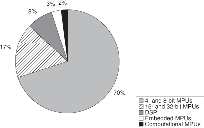
Clearly, controllers, embedded controllers, digital signal processors (DSPs), and so forth, are the dominant processor types, providing the focus for much of the processor design effort. If we look at the market growth, the same data show that the demand for SOC and larger microcontrollers is growing at almost three times that of microprocessor units (MPUs in Figure 3.2).
Figure 3.2 Annual growth in demand for microprocessors and controllers [227].

THIS CHAPTER AND PROCESSOR DETAILS
This chapter contains details about processor design issues, especially for advanced processors in high-performance applications. Readers selecting processors from established alternatives may choose to skip some of the details, such as sections about branch prediction and superscalar processor control. We indicate such sections with an asterisk (*) in the section title.
Such details are important, even for those selecting a processor, for two reasons:
1. Year by year, SOC processors and systems are becoming more complex. The SOC designer will be dealing with increasingly complex processors.
2. Processor performance evaluation tool sets (such as SimpleScalar [51]) provide options to specify issues such as branch prediction and related parameters.
Readers interested in application-specific instruction processors, introduced in Section 1.3, can find relevant material in Sections 6.3, 6.4, and 6.8.
Especially in SOC type applications, the processor itself is a small component occupying just a few percent of the die. SOC designs often use many different types of processors suiting the application. Often, noncritical processors are acquired (purchased) as design files (IP) and are integrated into the SOC design. Therefore, a specialized SOC design may integrate generic processor cores designed by other parties. Table 3.1 illustrates the relative advantages of different choices of using intellectual property within SOC designs.
TABLE 3.1 Optimized Designs Provide Better Area–Time Performance at the Expense of Design Time
| Type of Design | Design Level | Relative Expected Area × Time |
| Customized hard IP | Complete physical | 1.0 |
| Synthesized firm IP | Generic physical | 3.0–10.0 |
| Soft IP | RTL or ASIC | 10.0–100.0 |
3.2 PROCESSOR SELECTION FOR SOC
3.2.1 Overview
For many SOC design situations, the selection of the processor is the most obvious task and, in some ways, the most restricted. The processor must run a specific system software, so at least a core processor—usually a general-purpose processor (GPP)—must be selected for this function. In compute-limited applications, the primary initial design thrust is to ensure that the system includes a processor configured and parameterized to meet this requirement. In some cases, it may be possible to merge these processors, but that is usually an optimization consideration dealt with later. In determining the processor performance and the system performance, we treat memory and interconnect components as simple delay elements. These are referred to here as idealized components since their behavior has been simplified, but the idealization should be done in such a way that the resulting characterization is realizable. The idealized element is characterized by a conservative estimate of its performance.
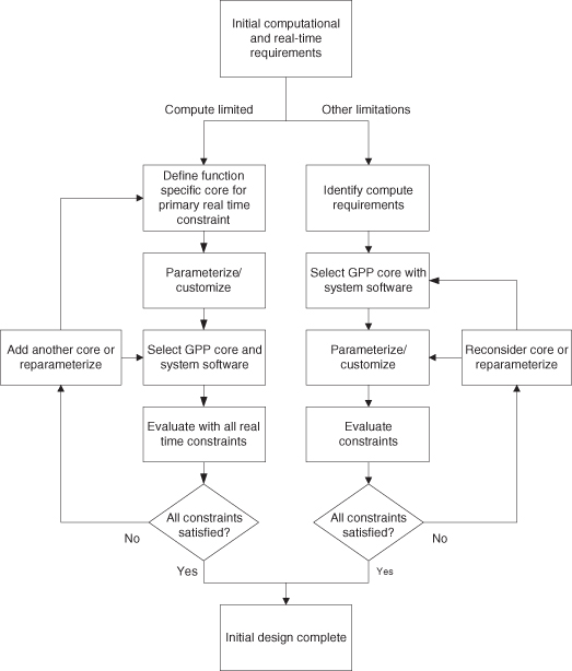
Figure 3.3 shows the processor model used in the initial design process. The process of selecting processors is shown in Figure 3.4. The process of selection is different in the case of compute-limited selection, as there can be a real-time requirement that must be met by one of the selected processors. This becomes a primary consideration at an early point in the initial SOC design phase. The processor selection and parameterization should result in an initial SOC design that appears to fully satisfy all functional and performance requirements set out in the specifications.
Figure 3.3 Processors in the SOC model.
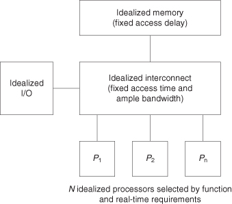
Figure 3.4 Process of processor core selection.
3.2.2 Example: Soft Processors
The term “soft core” refers to an instruction processor design in bitstream format that can be used to program a field programmable gate array (FPGA) device. The 4 main reasons for using such designs, despite their large area–power–time cost, are
1. cost reduction in terms of system-level integration,
2. design reuse in cases where multiple designs are really just variations on one,
3. creating an exact fit for a microcontroller/peripheral combination, and
4. providing future protection against discontinued microcontroller variants.
The main instruction processor soft cores include the following:
- Nios II [12]. Developed by Altera for use on their range of FPGAs and application-specific integrated circuits (ASICs).
- MicroBlaze [258]. Developed by Xilinx for use on their range of FPGAs and ASICs.
- OpenRISC [190]. A free and open-source soft-core processor.
- Leon [106]. Another free and open-source soft-core processor that implements a complete SPARC v8 compliant instruction set architecture (ISA). It also has an optional high-speed floating-point unit called GRFPU, which is free for download but is not open source and is only for evaluation/research purposes.
- OpenSPARC [235]. This SPARC T1 core supports single- and four-thread options on FPGAs.
There are many distinguishing features among all of these, but in essence, they support a 32-bit reduced instruction set computer (RISC) architecture (except OpenSPARC, which is 64 bits) with single-issue five-stage pipelines, have configurable data/instruction caches, and have support for the Gnu compiler collection (GCC) compiler tool chain. They also feature bus architectures suitable for adding extra processing units as slaves or masters that could be used to accelerate the algorithm, although some go further and allow the addition of custom instructions/coprocessors.
Table 3.2 contains a brief comparison of some of the distinguishing features of these different SOCs. It should be noted that the measurements for MIPS (million instructions per second) are mostly taken from marketing material and are likely to fluctuate wildly, depending on the specific configuration of a particular processor.
TABLE 3.2 Some Features of Soft-Core Processors
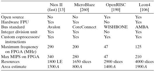
Now a simple comparison, we estimated in an earlier section that a 32-bit processor, without the floating-point unit, is around 60 A. We can see from Table 3.2 that such a processor is around 15–30 times smaller than soft processors.
3.2.3 Examples: Processor Core Selection
Let us consider two examples that illustrate the steps shown in Figure 3.4.
Example 1: Processor Core Selection, General Core Path
Consider the “other limitation” path in Figure 3.4 and look at some of the trade-offs. For this simple analysis, we shall ignore the processor details and just assume that the processor possibilities follow the AT2 rule discussed in Chapter 2. Assume that an initial design had performance of 1 using 100K rbe (register bit equivalent) of area, and we would like to have additional speed and functionality. So we double the performance (half the T for the processor). This increases the area to 400K rbe and the power by a factor of 8. Each rbe is now dissipating twice the power as before. All this performance is modulated by the memory system. Doubling the performance (instruction execution rate) doubles the number of cache misses per unit time. The effect of this on realized system performance depends significantly on the average cache miss time; we will see more of this in Chapter 4.
Suppose the effect of cache misses significantly reduces the realized performance; to recover this performance, we now need to increase the cache size. The general rule cited in Chapter 4 is to half the miss rate, we need to double the cache size. If the initial cache size was also 100K rbe, the new design now has 600K rbe and probably dissipates about 10 times the power of the initial design.
Is it worth it? If there is plenty of area while power is not a significant constraint, then perhaps it is worth it. The faster processor cache combination may provide important functionality, such as additional security checking or input/output (I/O) capability. At this point, the system designer refers back to the design specification for guidance.
Example 2: Processor Core Selection, Compute Core Path
Again refer to Figure 3.4, only now consider some trade-offs for the compute-limited path. Suppose the application is generally parallelizable, and we have several different design approaches. One is a 10-stage pipelined vector processor; the other is multiple simpler processors. The application has performance of 1 with the vector processor (area is 300K rbe) and half of that performance with a single simpler processor (area is 100K rbe). In order to satisfy the real-time compute requirements, we need to increase the performance to 1.5.
Now we must evaluate the various ways of achieving the target performance. Approach 1 is to increase the pipeline depth and double the number of vector pipelines; this satisfies the performance target. This increases the area to 600K rbe and doubles the power, while the clock rate remains unchanged. Approach 2 is to use an “array” of simpler interconnected processors. The multiprocessor array is limited by memory and interconnect contention (we will see more of these effects in Chapter 5). In order to achieve the target performance, we need to have at least four processors: three for the basic target and one to account for the overhead. The area is now 400K rbe plus the interconnect area and the added memory sharing circuitry; this could also add another 200K rbe. So we still have two approaches undifferentiated by area or power considerations.
So how do we pick one of these two alternatives? There are usually many more than two. Now all depends on the secondary design targets, which we only begin to list here:
1. Can the application be easily partitioned to support both approaches?
2. What support software (compilers, operating systems, etc.) exists for each approach?
3. Can we use the multiprocessor approach to gain at least some fault tolerance?
4. Can the multiprocessor approach be integrated with the other compute path?
5. Is there a significant design effort to realize either of the enhanced approaches?
Clearly, there are many questions the system designer must answer. Tools and analysis only eliminate the unsatisfactory approaches; after that, the real system analysis begins.
The remainder of this chapter is concerned with understanding the processor, especially at the microarchitecture level, and how that affects performance. This is essential in evaluating performance and in using simulation tools.
WAYS TO ACHIEVE PERFORMANCE
The examples used in Section 3.2 are quite simplistic. How does one create designs that match the AT2 design rule, or do even better? The secret is in understanding design possibilities, the freedom to choose among design alternatives. In order to do this, one must understand the complexity of the modern processor and all of its ramifications. This chapter presents a number of these alternatives, but it only touches the most important, and many other techniques can serve the designer well in specific situations. There is no substitute for understanding.
3.3 BASIC CONCEPTS IN PROCESSOR ARCHITECTURE
The processor architecture consists of the instruction set of the processor. While the instruction set implies many implementation (microarchitecture) details, the resulting implementation is a great deal more than the instruction set. It is the synthesis of the physical device limitations with area–time–power trade-offs to optimize specified user requirements.
3.3.1 Instruction Set
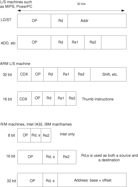
The instruction set for most processors is based upon a register set to hold operands and addresses. The register set size varies from 8 to 64 words or more, each word consisting of 32–64 bits. An additional set of floating-point registers (32–128 bits) is usually also available. A typical instruction set specifies a program status word, which consists of various types of control status information, including condition codes (CCs) set by the instruction. Common instruction sets can be classified by format differences into two basic types, the load–store (L/S) architecture and the register–memory (R/M) architecture:
- The L/S instruction set includes the RISC microprocessors. Arguments must be in registers before execution. An ALU instruction has both source operands and result specified as registers. The advantages of the L/S architecture are regularity of execution and ease of instruction decode. A simple instruction set with straightforward timing is easily implemented.
- The R/M architectures include instructions that operate on operands in registers or with one of the operands in memory. In the R/M architecture, an ADD instruction might sum a register value and a value contained in memory, with the result going to a register. The R/M instruction sets trace their evolution to the IBM mainframes and the Intel x86 series (now called the Intel IA32).
The trade-off in instruction sets is an area–time compromise. The R/M approach offers a more concise program representation using fewer instructions of variable size compared with L/S. Programs occupy less space in memory and require smaller instruction caches. The variable instruction size makes decoding more difficult. The decoding of multiple instructions requires predicting the starting point of each. The R/M processors require more circuitry (and area) to be devoted to instruction fetch and decode. Generally, the success of Intel-type x86 implementations in achieving high clock rates has shown that there is no decisive advantage of one approach over the other.
Figure 3.5 shows a general outline of some instruction layouts for typical machine instruction sets. RISC machines use a fixed 32-bit instruction size or a 32-bit format with 64-bit instruction extensions. Intel IA32 and the IBM System 390 (now called zSeries) mainframes use variable-size instructions. Intel uses 8-, 16-, and 32-bit instructions, while IBM uses 16-, 32-, and 48-bit instructions. Intel’s byte-sized instructions are possible because of the limited register set size. The size variability and the R/M format gave good code density, at the expense of decode complexity. The RISC-based ARM format is an interesting compromise. It offers a 32-bit instruction set with a built-in conditional field, so every instruction can be conditionally executed. It also offers a 16-bit instruction set (called the thumb instructions). The result offers both decode efficiency and code density.
Figure 3.5 Instruction size and format for typical processors.
Recent developments in instruction set extension will be covered in Chapter 6.
3.3.2 Some Instruction Set Conventions
Table 3.3 is a list of basic instruction operations and commonly used mnemonic representations. Frequently, there are different instructions for differing data types (integer and floating point). To indicate the data type that the operation specifies, the operation mnemonic is extended by a data-type indicator, so OP.W might indicate an OP for integers, while OP.F indicates a floating-point operation. Typical data-type modifiers are shown in Table 3.4. A typical instruction has the form OP.M destination, source 1, source 2. The source and destination specification has the form of either a register or a memory location (which is typically specified as a base register plus an offset)
TABLE 3.3 Instruction Set Mnemonic Operations
| Mnemonic | Operation |
| ADD | Addition |
| SUB | Subtraction |
| MPY | Multiplication |
| DIV | Division |
| CMP | Compare |
| LD | Load (a register from memory) |
| ST | Store (a register to memory) |
| LDM | Load multiple registers |
| STM | Store multiple registers |
| MOVE | Move (register to register or memory to memory) |
| SHL | Shift left |
| SHR | Shift right |
| BR | Unconditional branch |
| BC | Conditional branch |
| BAL | Branch and link |
TABLE 3.4 Data-Type Modifiers (OP.modifier)
| Modifier | Data Type |
| B | Byte (8 bits) |
| H | Halfword (16 bits) |
| W | Word (32 bits) |
| F | Floating point (32 bits) |
| D | Double-precision floating point (64 bits) |
| C | Character or decimal in an 8-bit format |
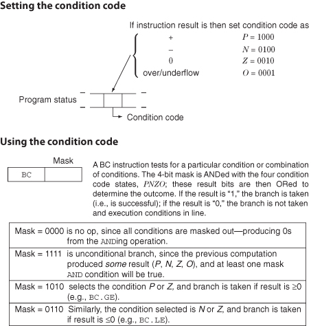
3.3.3 Branches
Branches (or jumps) manage program control flow. They typically consist of unconditional BR, conditional BC, and subroutine call and return (link). The BC tests the state of the CC, which usually consists of 4 bits in a program status or control register. Typically, the CC is set by an ALU instruction to record one of several results (encoded in 2 or 4 bits), for example, specifying whether the instruction has generated
1. a positive result,
2. a negative result,
3. a zero result, or
4. an overflow.
Figure 3.6 illustrates the use of CCs by the BC instruction. The unconditional branch (BR) is the BC with an all 1’s mask setting (see figure). It is possible (as in the ARM instruction set) to make all instructions conditional by including a mask field in each instruction.
Figure 3.6 Examples of BC instruction using the condition code.
3.3.4 Interrupts and Exceptions
Many embedded SOC controllers have external interrupts and internal exceptions, which indicate the need for attention by an interrupt manager (or handler) program. These facilities can be managed and supported in various ways:
1. User Requested versus Coerced. The former often covers erroneous execution, such as divide by zero, while the latter is usually triggered by external events, such as device failure.
2. Maskable versus Nonmaskable. The former type of event can be ignored by setting a bit in an interrupt mask, while the latter cannot be ignored.
3. Terminate versus Resume. An event such as divide by zero would terminate ordinary processing, while a processor resumes operation.
4. Asynchronous versus Synchronous. Interrupt events can occur in asynchrony with the processor clock by an external agent or not, as when caused by a program’s execution.
5. Between versus Within Instructions. Interrupt events can be recognized only between instructions or within an instruction execution.
In general, the first alternative of most of these pairs is easier to implement and may be handled after the completion of the current instruction. Whether the designer chooses to constrain the design only to precise exceptions, an exception is precise if all the instructions before the exception finish correctly, and all those after it do not change the state. Once the exception is handled, the latter instructions are restarted from scratch.
Moreover, some of these events may occur simultaneously and may even be nested. There is a need to prioritize them. Controllers and general-purpose processors have special units to handle these problems and preserve the state of the system in case of resuming exceptions.
3.4 BASIC CONCEPTS IN PROCESSOR MICROARCHITECTURE
Almost all modern processors use an instruction execution pipeline design. Simple processors issue only one instruction for each cycle; others issue many. Many embedded and some signal processors use a simple issue-one-instruction-per-cycle design approach. But the bulk of modern desktop, laptop, and server systems issue multiple instructions for each cycle.
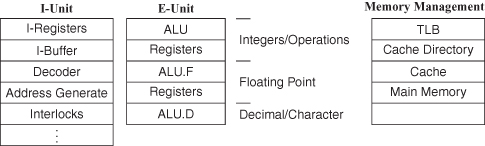
Every processor (Figure 3.7) has a memory system, execution unit (data paths), and instruction unit. The faster the cache and memory, the smaller the number of cycles required for fetching instructions and data (IF and DF). The more extensive the execution unit, the smaller the number of execution cycles (EX). The control of the cache and execution unit is done by the instruction unit.
Figure 3.7 Processor units.
The pipeline mechanism or control has many possibilities. Potentially, it can execute one or more instructions for each cycle. Instructions may or may not be decoded and/or executed in program order. Indeed, instructions from several different programs can be executed in the same cycle in multithreaded pipelines. Table 3.5 illustrates some of the possibilities.
TABLE 3.5 Types of Pipelined Processors
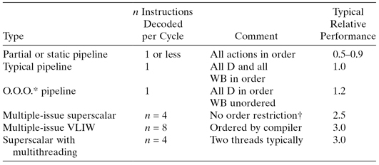
*Out of order (execution).
†Ordered only by dependencies.
Regardless of the type of pipeline, “breaks” or delays are the major limit on performance.
Pipeline delays or breaks generally arise from one of three causes:
1. Data Conflicts—Unavailability of a Source Operand. This can occur for several reasons; typically, the current instruction requires an operand that is the result of a preceding uncompleted instruction. Extensive buffering of operands can minimize this effect.
2. Resource Contention. Multiple successive instructions use the same resource or an instruction with a long execution time delays a successor instruction’s execution. Additional resources (floating-point units, register ports, and out-of-order execution) contribute to reducing contention.
3. Run-On Delays (in Order Execution Only). When instructions must complete the WB (writeback) in program order, any delay in execution (as in the case of multiply or divide) necessarily delays the instruction execution in the pipeline.
4. Branches. The pipeline is delayed because of branch resolution and/or delay in the fetching of the branch target instruction before the pipeline can resume execution. Branch prediction, branch tables, and buffers all can be used to minimize the effect of branches.
In the next section, we look at simple pipeline control and the operation of a basic pipeline. These simple processors have minimum complexity but suffer the most from (mostly branch) disruptions. Next, we consider the buffers that are required to manage data movement both through the pipeline and between units. Since the optimum pipeline layout (number of stages) is a strong function of the frequency of breaks, we look at branches and techniques for minimizing the effects of branch pipeline delays. Then, we look at multiple instruction execution and more robust pipeline control. Table 3.6 describes the architecture of some SOC processors.
TABLE 3.6 Processor Characteristics of Some SOC Designs
3.5 BASIC ELEMENTS IN INSTRUCTION HANDLING
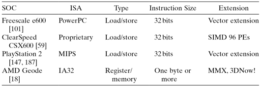
An instruction unit consists of the state registers as defined by the instruction set—the instruction register—plus the instruction buffer, decoder, and an interlock unit. The instruction buffer’s function is to fetch instructions into registers so that instructions can be rapidly brought into a position to be decoded. The decoder has the responsibility for controlling the cache, ALU, registers, and so on. Frequently, in pipelined systems, the instruction unit sequencing is managed strictly by hardware, but the execution unit may be microprogrammed so that each instruction that enters the execution phase will have its own microinstruction associated with it. The interlock unit’s responsibility is to ensure that the concurrent execution of multiple instructions has the same result as if the instructions were executed completely serially.
With instructions in various stages of execution, there are many design considerations and trade-offs in even simple pipelined processors.
Figure 3.8 shows the processor control or I-unit and basic communications paths to memory.
Figure 3.8 I-unit.
3.5.1 The Instruction Decoder and Interlocks
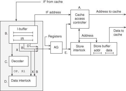
When an instruction is decoded, the decoder must provide more than control and sequencing information for that instruction. Proper execution of the current instruction depends on the other instructions in the pipeline. The decoder (Figure 3.9)
1. schedules the current instruction; the current instruction may be delayed if a data dependency (e.g., at the address generate or AG cycle) occurs or if an exception arises—for example, not in translation lookaside buffer (TLB) and cache miss;
2. schedules subsequent instructions; later instructions may be delayed to preserve in-order completion if, for example, the current instruction has multiple cycle execution; and
3. selects (or predicts) the path on branch instruction.
Figure 3.9 Decoder functions.
The data interlocks (subunit D in Figure 3.8) may be part of the decoder. This determines register dependencies and schedules the AG and EX units. The interlocks ensure that the current instruction does not use (depend on) a result of a previous instruction until that result is available.
The execution controller performs a similar function on subsequent instructions, ensuring that they do not enter the pipeline until the execution unit is scheduled to complete the current instruction, and, if required, preserve the execution order.
The effect of the interlocks (Figure 3.10) is that for each instruction as it is decoded, its source registers (for operands or addresses) must be compared (indicated by “C” in Figure 3.10) against the destination registers of previously issued but uncompleted instructions to determine dependencies. The opcode itself usually establishes the number of EX cycles required (indicated by the EX box in the figure). If this exceeds the number specified by the timing template, subsequent instructions must be delayed by that amount to preserve in-order execution.
Figure 3.10 Interlocks.

The store interlocks (E) perform the same function as the data interlocks for storage addresses. On STORE instructions, the address is sent to the store interlocks so that subsequent reads either from the AG (data reads) or the IB (instruction reads) can be compared with pending stores and dependencies detected.
3.5.2 Bypassing
Bypassing or forwarding is a data path that routes a result—usually from an ALU—to a user (perhaps also the ALU), bypassing a destination register (which is subsequently updated). This allows a result produced by the ALU to be used at an earlier stage in the pipeline than would otherwise be possible.
3.5.3 Execution Unit
As with the cache, the execution unit (especially the floating-point unit) can represent a significant factor in both performance and area. Indeed, even a straightforward floating-point unit can occupy as much or more area than a basic integer core processor (without cache). In simple in-order pipelines, the execution delay (run-on) can be a significant factor in determining performance. More robust pipelines use corresponding better arithmetic algorithms for both integer and floating-point operations. Some typical area–time trade-offs in floating-point units are shown in Table 3.7.
TABLE 3.7 Characteristics of Some Floating-Point Implementations

In the table, word size refers to the operand size (exponent and mantissa), and the IEEE standard 754 format is assumed. The execution time is the estimated total execution time in cycles. The pipelined column indicates the throughput: whether the implementation supports the execution of a new operation for each cycle. The final column is an estimate of the units of area needed for the implementation.
The minimal implementation would probably only support specialized applications and 32-bit operands. The typical implementation refers to the floating-point unit of a simple pipelined processor with 64-bit operands. Advanced processors support the extended IEEE format (80 bits), which protects the accuracy of intermediate computations. The multiple-issue implementation is a typical straightforward implementation. If the implementation is to support issue rates greater than four, the size could easily double.
3.6 BUFFERS: MINIMIZING PIPELINE DELAYS
Buffers change the way instruction timing events occur by decoupling the time at which an event occurs from the time at which the input data are used. It allows the processor to tolerate some delay without affecting the performance. Buffers enable latency tolerance as they hold the data awaiting entry into a stage.
Buffers can be designed for a mean request rate [115] or for a maximum request rate. In the former case, knowing the expected number of requests, we can trade off buffer size against the probability of an overflow. Overflows per se (where an action is lost) do not happen in internal CPU buffers, but an “overflow” condition—full buffer and a new request—will force the processor to slow down to bring the buffer entries down below buffer capacity. Thus, each time an overflow condition occurs, the processor pipeline stalls to allow the overflowing buffer to access memory (or other resources). The store buffer, for example, is usually designed for a mean request rate.
Maximum request rate buffers are used for request sources that dominate performance, such as in-line instruction requests or data entry in a video buffer. In this case, the buffer size should be sufficient to match the processor request rate with the cache or other storage service rate. A properly sized buffer allows the processor to continue accessing instructions or data at its maximum rate without the buffer running out of information.
3.6.1 Mean Request Rate Buffers
We assume that q is a random variable describing the request size (number of pending requests) for a resource; Q is the mean of this distribution; and σ is the standard deviation.
Little’s Theorem
The mean request size is equal to the mean request rate (requests per cycle), multiplied by the mean time to service a request [142].
We assume a buffer size of BF, and we define the probability of a buffer overflow as p. There are two upper bounds for p based on Markov’s and Chebyshev’s inequalities.
Markov’s Inequality
![]()
Chebyshev’s Inequality
![]()
Using these two inequalities, for a given probability of overflow (p), we can conservatively select BF, since either term provides an upper bound, as
EXAMPLE 3.1
Suppose we wish to determine the effectiveness of a two-entry write buffer. Assume the write request rate is 0.15 per cycle, and the expected number of cycles to complete a store is two. The mean request size is 0.15 × 2 = 0.3, using Little’s theorem. Assuming σ2 = 0.3 for the request size, we can calculate an upper bound on the probability of overflow as
![]()
3.6.2 Buffers Designed for a Fixed or Maximum Request Rate
A buffer designed to supply a fixed rate is conceptually easy to design. The primary consideration is masking the access latency. If we process one item per cycle and it takes three cycles to access an item, then we need to have a buffer space of at least three, or four, if we count the item being processed.
In general, the maximum rate buffer supplies a fixed rate of data or instructions for processing. There are many examples of such buffers, including the instruction buffer, video buffers, graphics, and multimedia buffers.
In the general case where s items are processed for each cycle, and p items are fetched from a storage with a fixed access time, the buffer size, BF is
![]()
The initial “1” is an allowance for a single entry buffer used for processing during the current cycle. In some cases, it may not be necessary. The buffer described here is designed to buffer entry into a functional unit or decoder (as an I decoder); it is not exactly the same as the frame buffer or the image buffer that manages transfers between the processor and a media device. However, the same principles apply in the design to these media buffers.
3.7 BRANCHES: REDUCING THE COST OF BRANCHES
Branches represent one of the difficult issues in optimizing processor performance. Typically, branches can significantly reduce performance. For example, the conditional branch instruction (BC) tests the CC set by a preceding instruction. There may be a number of cycles between the decoding of the branch and the setting of the CC (see Figure 3.11). The simplest strategy is for the processor to do nothing but simply to await the outcome of the CC set and to defer the decoding of the instruction following the BC until the CC is known. In case the branch is taken, the target is fetched during the time allocated to a data fetch in an arithmetic instruction. This policy is simple to implement and minimizes the amount of excess memory traffic created by branch instructions. More complicated strategies that attempt to guess a particular path will occasionally be wrong and will cause additional or excess instruction fetches from memory.
Figure 3.11 The delay caused by a branch (BC).

In Figure 3.11, the actual decode is five cycles late (i.e., a five-cycle branch penalty). This is not the whole effect, however. The timing of NEXT + 1 is delayed an additional cycle when the target path is taken, as this instruction has not been prefetched.
Since branches are a major limitation to processor performance [75, 222], there has been a great deal of effort to reduce the effect. There are two simple and two substantial approaches to the branch problem. The simple approaches are the following:
1. Branch Elimination. For certain code sequences, we can replace the branch with another operation.
2. Simple Branch Speedup. This reduces the time required for target instruction fetch and CC determination.
The two more complex approaches are generalizations of the simple approaches:
1. Branch Target Capture. After a branch has been executed, we can keep its target instruction (and its address) in a table for later use to avoid the branch delay. If we could predict the branch path outcome and had the target instruction in the buffer, there would be no branch delay.
2. Branch Prediction. Using available information about the branch, one can predict the branch outcome and can begin processing on the predicted program path. If the strategy is simple or trivial, for example, always fetch in-line on true conditional branches, it is called a fixed strategy. If the strategy varies by opcode type or target direction, it is called a static strategy. If the strategy varies according to current program behavior, it is called a dynamic strategy (see Figure 3.12).
Figure 3.12 Branch prediction.
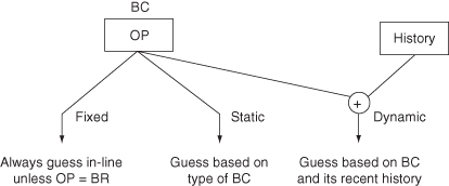
Table 3.8 summarizes these techniques. In the following sections, we look at two general approaches.
TABLE 3.8 Branch Management Techniques

3.7.1 Branch Target Capture: Branch Target Buffers (BTBs)
The BTB (Figure 3.13) stores the target instruction of the previous execution of the branch. Each BTB entry has the current instruction address (needed only if branch aliasing is a problem), the branch target address, and the most recent target instruction. (The target address enables the initiation of the target fetch earlier in the pipeline, since it is not necessary to wait for the address generation to complete.) The BTB functions as follows: Each instruction fetch indexes the BTB. If the instruction address matches the instruction addresses in the BTB, then a prediction is made as to whether the branch located at that address is likely to be taken. If the prediction is that the branch will occur, then the target instruction is used as the next instruction. When the branch is actually resolved, at the execute stage, the BTB can be updated with the corrected target information if the actual target differs from the stored target.
Figure 3.13 Branch target buffer (BTB) organization. The BTB is indexed by instruction bits. The particular branch can be confirmed (avoiding an alias) by referencing an instruction address field in the table.

The BTB’s effectiveness depends on its hit ratio—the probability that a branch is found in the BTB at the time it is fetched. The hit rate for a 512-entry BTB varies from about 70% to over 98%, depending on the application.
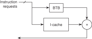
BTBs can be used in conjunction with the I-cache. Suppose we have a configuration as shown in Figure 3.14. The IF is made to both the BTB and I-cache. If the IF “hits” in the BTB, the target instruction that was previously stored in the BTB is now fetched and forwarded to the processor at its regularly scheduled time. The processor will begin the execution of the target instruction with no branch delay.
Figure 3.14 Typical BTB structure. If “hit” in the BTB, then the BTB returns the target instruction to the processor; CPU guesses the target. If “miss” in the BTB, then the cache returns the branch and in-line path; CPU guesses in-line.
The BTB provides both the target instruction and the new PC. There is now no delay on a taken branch so long as the branch prediction is correct. Note that the branch itself must still be fetched from the I-cache and must be fully executed. If either the AG outcome or the CC outcome is not as expected, all instructions in the target fetch path must be aborted. Clearly, no conditionally executed (target path) instruction can do a final result write, as this would make it impossible to recover in case of a misprediction.
3.7.2 Branch Prediction
Beyond the trivial fixed prediction, there are two classes of strategies for guessing whether or not a branch will be taken: a static strategy, which is based upon the type of branch instruction, and a dynamic strategy, which is based upon the recent history of branch activity.
Even perfect prediction does not eliminate branch delay. Perfect prediction simply converts the delay for the conditional branch into that for the unconditional branch (branch taken). So, it is important to have BTB support before using a more robust (and expensive) predictor.
Static Prediction
Static prediction is based on the particular branch opcode and/or the relative direction of the branch target. When a branch is decoded, a guess is made on the outcome of the branch, and if it is determined that the branch will be successful, the pipeline fetches the target instruction stream and begins decoding from it. A simple approach is shown in Table 3.9.
TABLE 3.9 A Static Branch Prediction Strategy

*When the branch target is less than the current PC, assume a loop and take the target. Otherwise, guess in-line.
The general effectiveness of a strategy described in Table 3.9 is typically 70–80%.
Dynamic Prediction: Bimodal
Dynamic strategies make predictions based on past history; that is, the sequence of past actions of a branch—was it or was it not taken? Table 3.10 from Lee and Smith [154] shows the effectiveness of a branch prediction when prediction is based on a count of the outcome of preceding executions of the branch in question. The prediction algorithm is quite simple. In implementing this scheme, a small up/down saturating counter is used. If the branch is taken, the counter is incremented up to a maximum value (n). An unsuccessful branch decrements the counter. In a 2-bit counter, the values 00 and 01 would predict a branch not taken, while 10 and 11 predicts a branch taken. The table can be separate or integrated into a cache is shown in Figure 3.15.
TABLE 3.10 Percentage Correct Guess Using History with n-bit Counters [154]
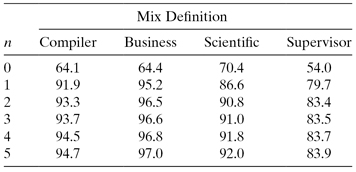
Figure 3.15 Branch history counter can be kept in I-cache (above) or in a separate table.
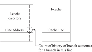
Depending on the table organization, two branches can map into the same history, creating an aliasing problem.
A number of observations can be made from Table 3.10. First, the predictive accuracy very closely approaches its maximum with just a few bits. Second, the predictive accuracy for a two bit counter varies from 83.4% to 96.5%, which is much higher than the accuracy using only the branch opcode prediction strategy of Table 3.9. Third, the effectiveness of prediction in a standard test suite (SPECmarks) is reported to be 93.5% using a very large table.
Dynamic Prediction: Two-Level Adaptive
Bimodal prediction is generally limited to prediction rates around 90% across multiple environments. Yeh and Patt [267, 268] have looked at adaptive branch prediction as a method of raising prediction rates to 95%. The basic method consists of associating a shift register with each branch in, for example, a branch table buffer. The shift register records branch history. A branch twice taken and twice not taken, for example, would be recorded as “1100.” Each pattern acts as an address into an array of counters, such as the 2-bit saturating counters. Each time the pattern 1100 is encountered, the outcome is recorded in the saturating counter. If the branch is taken, the counter is incremented; if the branch is not taken, it is decremented.
Adaptive techniques can require a good deal of support hardware. Not only must we have history bits associated with the possible branch entries but we must also have a table of counters to store outcomes. The approach is more effective in large programs where it is possible to establish a stable history pattern.
The average trace data from Yeh and Patt indicates that an adaptive strategy using a 6-bit entry provided a 92% correct prediction rate increasing to 95% with a 24-bit entry. Notice that the published SPECmark performance is significantly higher than other data.
The 2-bit saturating counter achieves 89.3% averaged over all programs. However, the data in Figure 3.16 is based on a different set of programs than those presented in Table 3.10.
Figure 3.16 Branch prediction rates for a two-level adaptive predictor.
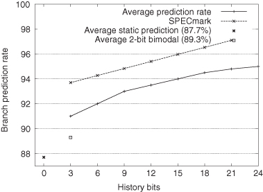
The adaptive results are shown for the prediction rate averaged over all programs [267]. Differences between 89% and 95% may not seem significant, but overall execution delay is often dominated by mispredicted branches.
Dynamic Prediction: Combined Methods
The bimodal and the adaptive approaches provide rather different information about the likelihood of a branch path. Therefore, it is possible to combine these approaches by adding another (vote) table of (2-bit saturating) counters. When the outcomes differ, the vote table selects between the two, and the final result updates the count in the vote table. This is referred to as combined prediction method and offers an additional percent or so improvement in the prediction rate. Of course, one can conceive of combining more than two predictions for an even more robust predictor.
The disadvantage of the two-level approach includes the hardware requirement for control and two serial table accesses. An approximation to it is called the global adaptive predictor. It uses only one shift register for all branches (global) to index into a single history table. While faster than the two-level in prediction, its prediction accuracy is only comparable to the bimodal predictor. But one can combine the bimodal predictor with the global adaptive predictor to create an approximate combined method. This gives results comparable to the two-level adaptive predictor.
Some processor branch strategies are shown in Table 3.11. Some SOC type processor branch strategies are shown in Table 3.12; they are notably simpler than workstation processors.
TABLE 3.11 Some Typical Branch Strategies
| Workstation Processors | Prediction Method | Target Location |
| AMD | Bimodal: 16K × 2 bit | BTB: 2K entries |
| IBM G5 | Three tables combined method | BTB |
| Intel Itanium | Two-level adaptive | Targets in I-cache with branch |
| SOC processors | Prediction method | Target location |
| Intel XScale (ARM v5) | History bits | BTB: 128 entries |
TABLE 3.12 Branch Prediction Strategies of Some SOC Designs

3.8 MORE ROBUST PROCESSORS: VECTOR, VERY LONG INSTRUCTION WORD (VLIW), AND SUPERSCALAR
To go beyond one cycle per instruction (CPI), the processor must be able to execute multiple instructions at the same time. Concurrent processors must be able to make simultaneous accesses to instruction and data memory and to simultaneously execute multiple operations. Processors that achieve a higher degree of concurrency are called concurrent processors, short for processors with instruction-level concurrency.
For the moment, we restrict our attention to those processors that execute only from one program stream. They are uniprocessors in that they have a single instruction counter, but the instructions may have been significantly rearranged from the original program order so that concurrent instruction execution can be achieved.
Concurrent processors are more complex than simple pipelined processors. In these processors, performance depends in greater measure on compiler ability, execution resources, and memory system design. Concurrent processors depend on sophisticated compilers to detect the instruction-level parallelism that exists within a program. The compiler must restructure the code into a form that allows the processor to use the available concurrency. Concurrent processors require additional execution resources, such as adders and multipliers, as well as an advanced memory system to supply the operand and instruction bandwidth required to execute programs at the desired rate [208, 250].
3.9 VECTOR PROCESSORS AND VECTOR INSTRUCTION EXTENSIONS
Vector instructions boost performance by
1. reducing the number of instructions required to execute a program (they reduce the I-bandwidth);
2. organizing data into regular sequences that can be efficiently handled by the hardware; and
3. representing simple loop constructs, thus removing the control overhead for loop execution.
Vector processing requires extensions to the instruction set, together with (for best performance) extensions to the functional units, the register sets, and particularly to the memory of the system.
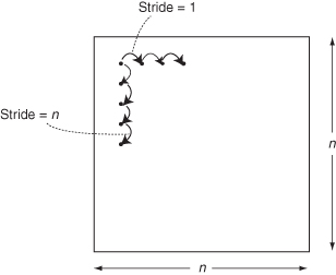
Vectors, as they are usually derived from large data arrays, are the one data structure that is not well managed by a conventional data cache. Accessing array elements, separated by an addressing distance (called the stride), can fill a smaller- to intermediate-sized data cache with data of little temporal locality; hence, there is no reuse of the localities before the items must be replaced (Figure 3.17).
Figure 3.17 For an array in memory, different accessing patterns use different strides in accessing memory.
Vector processors usually include vector register (VR) hardware to decouple arithmetic processing from memory. The VR set is the source and destination for all vector operands. In many implementations, accesses bypass the cache. The cache then contains only scalar data objects—objects not used in the VRs (Figure 3.18).
Figure 3.18 The primary storage facilities in a vector processor. Vector LD/ST usually bypasses the data cache.

3.9.1 Vector Functional Units
The VRs typically consist of eight or more register sets, each consisting of 16–64 vector elements, where each vector element is a floating-point word.
The VRs access memory with special load and store instructions. The vector execution units are usually arranged as an independent functional unit for each instruction class. These might include
- add/subtract,
- multiplication,
- division or reciprocal, and
- logical operations, including compare.
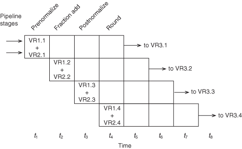
Since the purpose of the vector vocabulary is to manage operations over a vector of operands, once the vector operation is begun, it can continue at the cycle rate of the system. Figure 3.19 shows timing for a sample four-stage functional pipeline. A vector add (VADD) sequence passes through various stages in the adder. The sum of the first elements of VR1 and VR2 (labeled VR1.1 and VR2.1) are stored in VR3 (actually, VR3.1) after the fourth adder stage.
Figure 3.19 Approximate timing for a sample four-stage functional pipeline.
Pipelining of the functional units is more important for vector functional units than for scalar functional units, where latency is of primary importance.
The advantage of vector processing is that fewer instructions are required to execute the vector operations. A single (overlapped) vector load places the information into the VRs. The vector operation executes at the clock rate of the system (one cycle per executed operand), and an overlapped vector store operation completes the vector transaction overlapped with subsequent instruction operations (see Figure 3.20). Vector loads (VLD) must complete before they can be used (Figure 3.21), since otherwise the processor would have to recognize when operands are delayed in the memory system.
Figure 3.20 For logically independent vector instructions, the number of access paths to the vector register (VR) set and vector units may limit performance. If there are four read ports, the vector multiply (VMPY) can start on the second cycle. Otherwise, with two ports, the VMPY must wait until the VADD completes use of the read ports.
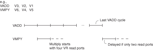
Figure 3.21 While independent VLD and VADD may proceed concurrently (with sufficient VR ports), operations that use the results of VLD do not begin until the VLD is fully complete.
The ability of the processor to concurrently execute multiple (independent) vector instructions is also limited by the number of VR ports and vector execution units. Each concurrent vector load or store requires a VR port; vector ALU operations require multiple ports.
Under some conditions, it is possible to execute more than one vector arithmetic operation per cycle. As with bypassing, the results of one vector arithmetic operation can be directly used as an operand in subsequent vector instructions without first passing into a VR. Such an operation, shown in Figures 3.22 and 3.23, is called chaining. It is illustrated in Figure 3.22 by a chained ADD-MPY with each functional unit having four stages. If the ADD-MPY were unchained, it would take 4 (startup) + 64 (elements/VR) = 68 cycles for each instruction—a total of 136 cycles. With chaining, this is reduced to 4 (add startup) + 4 (multiply startup) + 64 (elements/VR) = 72 cycles.
Figure 3.22 Effect of vector chaining.
Figure 3.23 Vector chaining path.

One of the crucial aspects in achieving the performance potential of the vector processor is the management of references to memory. Since arithmetic operations complete one per cycle, a vector code makes repeated references to memory to introduce new vectors in the VRs and to write out old results. Thus, on the average, memory must have sufficient bandwidth to support at least a two-words-per-cycle execution rate (one read and one write), and preferably three references per cycle (two reads and one write). This bandwidth allows for two vector reads and one vector write to be initiated and executed concurrently with the execution of a vector arithmetic operation. If there is insufficient memory bandwidth from memory to the VRs, the processor necessarily goes idle after the vector operation until the vector loads and stores are complete. It is a significant challenge to the designer of a processor not to simply graft a vector processing extension onto a scalar processor design but rather to adapt the scalar design—especially the memory system—to accommodate the requirements of fast vector execution (Table 3.13). If the memory system bandwidth is insufficient, there is correspondingly less performance improvement from the vector processing hardware.
TABLE 3.13 Potential Memory Requirements (Number of Accesses/Processor Cycles)
| I | D | |
| Scalar unit | 1.0−* | 1.0* |
| Vector unit | 0.0+† | 2.0–3.0‡ |
*Nominally. Reduced by I-buffer, I-cache.
†Relatively small compared to other requirements.
‡The minimum required is one vector load (VLD) and one vector store (VST) concurrently; preferably two VLDs and one VST, all concurrently.
The major elements of the vector processor are shown in (Figure 3.24). The functional units (add, multiply, etc.) and the two register sets (vector and scalar, or general) are connected by one or more bus sets. If chaining (Figure 3.23) is allowed, then three (or more) source operands are simultaneously accessed from the VRs and a result is transmitted back to the VRs. Another bus couples the VRs and the memory buffer. The remaining parts of the system—I-cache, D-cache, general registers, and so on—are typical of pipelined processors.
Figure 3.24 Major data paths in a generic vector processor.
3.10 VLIW PROCESSORS
There are two broad classes of multiple-issue machines: statically scheduled and dynamically scheduled. In principle, these two classes are quite similar. Dependencies among groups of instructions are evaluated, and groups found to be independent are simultaneously dispatched to multiple execution units. For statically scheduled processors, this detection process is done by the compiler, and instructions are assembled into instruction packets, which are decoded and executed at run time. For dynamically scheduled processors, the detection of independent instructions may also be done at compile time and the code can be suitably arranged to optimize execution patterns, but the ultimate selection of instructions (to be executed or dispatched) is done by the hardware in the decoder at run time. In principle, the dynamically scheduled processor may have an instruction representation and form that is indistinguishable from slower pipeline processors. Statically scheduled processors must have some additional information either implicitly or explicitly indicating instruction packet boundaries.
As mentioned in Chapter 1, early VLIW machines [92] are typified by processors from Multiflow and Cydrome. These machines use an instruction word that consists of 10 instruction fragments. Each fragment controls a designated execution unit; thus, the register set is extensively multiported to support simultaneous access to the multiplicity of execution units. In order to accommodate the multiple instruction fragments, the instruction word is typically over 200 bits long (see Figure 3.25). In order to avoid the obvious performance limitations imposed by the occurrence of branches, a novel compiler technology called trace scheduling was developed. By use of trace scheduling, the dynamic frequency of branching is greatly reduced. Branches are predicted where possible, and on the basis of the probable success rate, the predicted path is incorporated into a larger basic block. This process continues until a suitably sized basic block (code without branches) can be efficiently scheduled. If an unanticipated (or unpredicted) branch occurs during the execution of the code, at the end of the basic block, the proper result is fixed up for use by a target basic block.
Figure 3.25 A partial VLIW format. Each fragment concurrently accesses a single centralized register set.
More recent attempts at multiple-issue processors have been directed at rather lower amounts of concurrency. However there has been increasing use of simultaneous multithreading (SMT). In SMT, multiple programs (threads) use the same processor execution hardware (adders, decoders, etc.) but have their own register sets and instruction counter and register. Two processors (or cores) on the same die each using two-way SMT allows four programs to be in simultaneous execution.
Figure 3.26 shows the data paths for a generic VLIW machine. The extensive use of register ports provides simultaneous access to data as required by a VLIW processor. This suggests the register set may be a processor bottleneck.
Figure 3.26 Major data paths in a generic VLIW processor.
3.11 SUPERSCALAR PROCESSORS
Superscalar processors can also be implemented by the data paths shown in Figure 3.26. Usually, such processors use multiple buses connecting the register set and functional units, and each bus services multiple functional units. This may limit the maximum degree of concurrency but can correspondingly reduce the required number of register ports.
The issue of detection of independence within or among instructions is theoretically the same regardless of whether the detection process is done statically or dynamically (although the realized effect is quite different). In the next sections, we review the theory of instruction independence. In superscalar processors, detection of independence must be done in hardware. This necessarily complicates both the control hardware and the options in realizing the processor. The remaining discussion in this section is somewhat more detailed and complex than the discussion of other approaches.
3.11.1 Data Dependencies
With out-of-order execution, three types of dependencies are possible between two instructions, Ii and Ij (i precedes j in execution sequence). The first, variously called a read-after-write (RAW) dependency or an essential dependency, arises when the destination of Ii is the same as the source of Ij:
![]()
![]()
This is a data or address dependency.
Another condition that causes a dependency occurs when the destination of instruction Ij is the same as the source of a preceding instruction Ii. This occurs when
![]()
![]()
This arises when an instruction in sequence is delayed and a following instruction is allowed to precede in execution order and to change the contents of one of the original instruction’s source registers; as in the following example (R3 is the destination),
Instruction 2 is delayed by a divide operation in instruction 1. If instruction 3 is allowed to execute as soon as its operands are available, this might change the register (R3) used in the computation of instruction 2. A dependency of this type is called a write-after-read (WAR) dependency or an ordering dependency, since it only happens when out-of-order execution is allowed.
In the final type of dependency, the destination of instruction Ii, is the same as the destination of instruction Ij, or
![]()
In this case, instruction Ii could complete after instruction Ij, and the result in the register is that of instruction Ii when it ought to be that of Ij. This dependency, called a write-after-write (WAW) dependency or an output dependency, is somewhat debatable. If instruction Ii produces a result that is not used by an instruction that follows it until instruction Ij produces a new result for the same destination, then instruction Ii was unnecessary in the first place Figure 3.27. As this type of dependency is generally eliminated by an optimizing compiler, it can be largely ignored in our discussions. We illustrate this with two examples:
Example #1

Example #2
Figure 3.27 Detecting independent instructions.
The first example is a case of a redundant instruction (the DIV), whereas the second has an output dependency, but also has an essential dependency; once this essential dependency is dealt with, the output dependency is also covered. The fewer the dependencies that arise in the code, the more concurrency available in the code and the faster the overall program execution.
3.11.2 Detecting Instruction Concurrency
Detection of instruction concurrency can be done at compile time, at run time (by the hardware), or both. It is clearly best to use both the compiler and the run-time hardware to support concurrent instruction execution. The compiler can unroll loops and generally create larger basic block sizes, reducing branches. However, it is only at run time that the complete machine state is known. For example, an apparent resource dependency created by a sequence of divide, load, divide instructions may not exist if, say, the intervening load instruction created a cache miss.
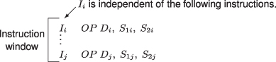
Instructions are checked for dependencies during decode. If an instruction is found to be independent of other, earlier instructions, and if there are available resources, the instruction is issued to the functional unit. The total number of instructions checked determines the size of the instruction window (Figure 3.28). Suppose the instruction window has N instructions, and at any given cycle M instructions are issued. In the next cycle, the successor M instructions are brought into the buffer, and again N instructions are checked. Up to M instructions may be issued in a single cycle.
Figure 3.28 Instruction window.

Ordering and output dependencies can be eliminated with sufficient registers. When either of these dependencies is detected it is possible to rename the dependent register to another register usually not available to the instruction set. This type of renaming requires that the register set be extended to include rename registers. A typical processor may extend a 32-register set specified by the instruction set to a set of 45–60 total registers, including the rename registers (for SOC processor usage see Table 3.14).
TABLE 3.14 Renaming Characteristics of Some SOC Designs
| SOC | Renaming Buffer Size | Reservation Station Number |
| Freescale e600 | 16 GPR, 16 FPR, 16 VR | 8 |
| MIPS 74K | 32 CB | — |
GPR, general-purpose register; FPR, floating-point register; VR, vector register; CB, completion buffer.
Figure 3.29 illustrates the overall layout of an M pipelined processor inspecting N instructions and issuing M instructions.
Figure 3.29 An M pipelined processor.
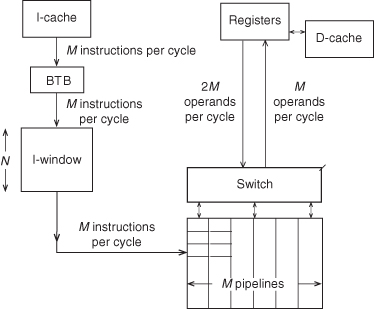
Any of the N instructions in the window are candidates for issue, depending on whether they are independent and whether there are execution resources available.
If the processor, for example, can only accommodate two L/S instructions, a floating-point instruction, and a fixed-point instruction, then the decoder in the instruction window must select these types of instructions for issue. So three L/S instructions could not be issued even if they were all independent.
Scheduling is the process of assigning specific instructions and their operand values to designated resources at designated times. Scheduling can be done either centrally or in a distributed manner by the functional units themselves at execution time. The former approach is called control flow scheduling; the latter is called dataflow scheduling. In control flow scheduling, dependencies are resolved during the decode cycle and the instructions are held (not issued) until the dependencies have been resolved. In a dataflow scheduling system, the instructions leave the decode stage when they are decoded and are held in buffers at the functional units until their operands and the functional unit are available.
Early machines used either control flow or dataflow to ensure correct operation of out-of-order instructions. The CDC 6600 [242] used a control flow approach. The IBM 360 Model 91 [246] was the first system to use dataflow scheduling.
3.11.3 A Simple Implementation
In this section, we look at a simple scheduling implementation. While it uses N = 1 and M = 1, it allows out-of-order execution and illustrates a basic strategy in managing dependencies.
Consider a system with multiple functional units, each of whose executions may involve multiple cycles. Using the L/S architecture as our model, we assume that there is a centralized single set of registers that provide operands for the functional units.
Suppose there are up to N instructions already dispatched for execution, and we must determine how to issue an instruction currently at the decoder. Issuing a single instruction in the presence of up to N − 1 unissued previous instructions is equivalent to issuing that instruction as the last of N instructions issued at one time.
We use an approach sometimes referred to as the dataflow approach or a tag-forwarding approach. It was first suggested by Tomasulo [246], and it is also known by his name.
Each register in the central register set is extended to include a tag that identifies the functional unit that produces a result to be placed in a particular register. Similarly, each of the multiple functional units has one or more reservation stations (Figure 3.30).
Figure 3.30 Reservation stations are associated with function units. They contain instruction opcode and data values or a tag corresponding to a data value pending entry into a functional unit. They perform the function of a rename register.
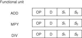
The reservation station contains either a tag identifying another functional unit or register, or it can contain the value needed. Operand values for a particular instruction need not be available for the instruction to be issued to the reservation station; the tag of a particular register may be substituted for a value, in which case the reservation station waits until the value is available. Since the reservation station holds the current value of the available data, it acts as a rename register, and thus the scheme avoids ordering and output dependencies.
Control is distributed within the functional units. Each reservation station effectively defines its own functional unit; thus, two reservations for a floating-point multiplier are two functional unit tags: multiplier 1 and multiplier 2 (Figure 3.31). If operands can go directly into the multiplier, then there is another tag: multiplier 3. Once a pair of operands has a designated functional unit tag, that tag remains with that operand pair until the completion of the operation. Any unit (or register) that depends on that result has a copy of the functional unit tag and ingates the result that is broadcast on the bus.
Figure 3.31 Dataflow. Each reservation station consists of registers to hold S1 and S2 values (if available), or tags to identify where the values come from.

For the preceding example,

The DIV.F is initially issued to the divide unit with values from R1 and R2. (Assuming they are available, they are fetched from the common bus.) A divide unit tag is issued to R3, indicating that it does not currently contain a valid value. On the next cycle, the MPY.F is issued to the multiply unit, together with the value from R4 and a TAG [DIV] from R3. When the divide unit completes, it broadcasts its result; this is ingated into the multiply unit reservation station, since it is holding a “divide unit” tag. In the meantime, the add unit has been issued values from R6 and R7 and commences addition. R4 gets the tag from the adder; no ordering dependency occurs since the multiplier already has the old value of R4.
In the dataflow approach, the results to a targeted register may never actually go to that register; in fact, the computation based on the load of a particular register may be continually forwarded to various functional units, so that before the value is stored, a new value based upon a new computational sequence (a new load instruction) is able to use the targeted register. This approach partially avoids the use of a central register set, thereby avoiding the register ordering and output dependencies.
Whether the ordering and output dependencies are a serious problem or not is the subject of some debate [228]. With a larger register set, an optimizing compiler can distribute the usage of the registers across the set and avoid the register–resource dependencies. Of course, all schemes are left with the essential (type 1) dependency. Large register sets may have their own disadvantages, however, especially if save and restore traffic due to interrupts becomes a significant consideration.
As far as implementation is concerned, the issue logic is distributed in the reservation stations. When multiple instructions are to be issued in the same cycle, then there must be multiple separate buses to transmit the information: operation, tag/value #1, tag/value #2, and destination. We assume that the reservation stations are associated with the functional units. If we centralize the reservation stations for implementation convenience, the design would be generally similar to an improved control flow, or scoreboard.
Action Summary
We can summarize the basic rules:
1. The decoder issues instructions to a functional unit reservation station with data values if available otherwise with register tag.
2. The destination register (specified by instruction) gets the functional unit tag.
3. Continue issue until a type of reservation station is FULL. Unissued instructions are held PENDING.
4. Any instruction that depends on an unissued or pending instruction must also be held in a pending state.
3.11.4 Preserving State with Out-of-Order Execution
Out-of-order execution leads to an apparently ill-defined machine state, even as the code is executing correctly. If an interrupt arises or some sort of an exception is taken (perhaps even a misguessed branch outcome), there can be a general ambiguity as to the exact source of the exception or how the machine state should be saved and restored for further instruction processing. There are two basic approaches to this problem:
1. Restrict the programmer’s model. This applies only to interrupts and involves the use of a device called an imprecise interrupt, which simply indicates that an exception has occurred someplace in some region of code without trying to isolate it further. This simple approach may be satisfactory for signal or embedded processors that use only real (no virtual) memory but is generally unacceptable for virtual memory processors.
A load instruction that accesses a page not currently in memory can have disastrous consequences if several instructions that followed it are already in execution. When control returns to the process after the missing page is loaded, the load can execute together with instructions that depended upon it, but other instructions that were previously executed should not be re-executed. The control for all this can be formidable. The only acceptable alternative would be to require that all pages used by a particular process be resident in memory before execution begins. In programming environments where this is feasible and practical, such as in large scientific applications, this may be a solution.
2. Create a write-back that preserves the ordered use of the register set or at least allows the reconstruction of such an ordered register set.
In order to provide a sequential model of program execution, some mechanism must be provided that properly manages the register file state. The key to any successful scheme [135, 221] is the efficient management of the register set and its state. If instructions execute in order, then results are stored in the register file (Figure 3.32). Instructions that can complete early must be held pending the completion of previously issued but incomplete instructions. This sacrifices performance.
Figure 3.32 Simple register file organization.

Another approach uses a reorder buffer (Figure 3.33). The results arrive at the reorder buffer out of program sequence, but they are written back to the sequential register file in program order, thus preserving the register file state. In order to avoid conflicts at the reorder buffer, we can distribute the buffer across the various functional units as shown in Figure 3.34. Either of these techniques allows out-of-order instruction execution but preserves in-order write-back to the register set.
Figure 3.33 Centralized reorder buffer method.

Figure 3.34 Distributed reorder buffer method.

3.12 PROCESSOR EVOLUTION AND TWO EXAMPLES
We bring the concepts of the earlier sections together with a few observations and then by looking at an example of a currently available high-performance processor.
3.12.1 Soft and Firm Processor Designs: The Processor as IP
Processor designs for use in SOC and other application-specific areas require more than just generic processor concepts. The designer is still faced with achieving the best possible performance for a given number of transistors. The object is to have efficient, modular designs that can be readily adapted to a number of situations. The better designs have
1. an instruction set that makes efficient use of both instruction memory (code density) and data memory (several operand sizes);
2. an efficient microarchitecture that maintains performance across a broad range of applications;
3. a relatively simple base structure that is economical in its use of transistors;
4. a selected number of coprocessor extensions that can be readily added to the base processor; these would include floating-point and vector coprocessors; and
5. full software support for all processor configurations; this includes compilers and debuggers.
A classic example of this type of processor design is the ARM 1020. It uses an instruction set with both 16- and 32-bit instructions for improved code density. The data paths for the 1020T are shown in Figure 3.35. A debug and system control coprocessor and/or a vector and floating-point coprocessor can be added directly for enhanced performance. The ARM bus is also a standard for SOC use.
Figure 3.35 ARM 1020 data paths [20].

The instruction timing is a quite simple six-stage pipeline as shown in Figure 3.36. Because of its simplicity, it can achieve close to its peak performance of one instruction for each cycle (ignoring cache misses).
Figure 3.36 The ARM pipeline.

3.12.2 High-Performance, Custom-Designed Processors
When the target is high-performance workstations, design effort is a secondary issue to performance (but not to time-to-market). The result is that large teams of designers focus on custom circuitry, clocking, algorithms and microarchitecture to achieve performance on a schedule. An example is the Freescale e600 (Figure 3.37). Such processors use all the design techniques discussed in this chapter plus others:
1. With lots of area (transistors) available, we would expect to see large branch tables, multiple execution units, multiple instruction issue, and out-of-order instruction completion.
2. With increased clock rates and a shorter cycle time, we would expect to see some basic operations (e.g., I fetch) to take more than one cycle. Overall, with shorter clocks and a much more elaborate pipeline, the timing template is significantly longer (a larger number of steps).
3. Since large caches have a long access time, we would expect to see small first-level caches supported by a hierarchy of one or more levels of increasing larger caches.
Figure 3.37 Freescale e600 data paths [101].
3.13 CONCLUSIONS
Pipelined processors have become the implementation of choice for almost all machines from mainframes to microprocessors. High-density VLSI logic technology, coupled with high-density memory, has made possible this movement to increasingly complex processor implementations.
In modeling the performance of pipelined processors, we generally allocate a basic quantum of time for each instruction and then add to that the expected delays due to dependencies that arise in code execution. These dependencies usually arise from branches, dependent data, or limited execution resources. For each type of dependency, there are implementation strategies that mitigate the effect of the dependency. Implementing branch prediction strategies, for example, mitigates the effect of branch delays. Dependency detection comes at the expense of interlocks, however. The interlocks consist of logic associated with the decoder to detect dependencies and to ensure proper logical operation of the machine in executing code sequences.
3.14 PROBLEM SET
1. Following Study 3.1, show the timing for the following three instruction sequences:

Study 3.1 Sample Timing
For the code sequence

assume three separate floating-point units with execution times:
| Divide | Eight cycles |
| Multiply | Four cycles |
| Add | Three cycles |
and show the timing for a dataflow.
For this approach, we might have the following:
| Cycle 1 | Decoder issues I1 → DIV unit | |
| R1 → DIV Res Stn | ||
| R2 → DIV Res Stn | ||
| TAG_DIV → R3 | ||
| Cycle 2 | Begin DIV.F | |
| Decoder issues I2 → MPY unit | ||
| TAG_DIV → MPY unit | ||
| R4 → MPY Res Stn | ||
| TAG_MPY → R5 | ||
| Cycle 3 | Multiplier waits | |
| Decoder issues I3 → ADD unit | ||
| R6 → ADD Res Stn | ||
| R7 → ADD Res Stn | ||
| TAG_ADD → R4 | ||
| Cycle 4 | Begin ADD.F | |
| Cycle 6 | ADD unit requests broadcast next cycle (granted). | |
| ADD unit completes this cycle. | ||
| Cycle 7 | ADD unit result → R4 | |
| Cycle 9 | DIV unit requests broadcast next cycle (granted). | |
| DIV unit completes this cycle. | ||
| Cycle 10 | DIV unit → R3 | |
| DIV unit → MPY unit | ||
| Cycle 11 | Begin MPY.F | |
| Cycle 14 | Multiply completes and requests data broadcast (granted). | |
| Cycle 15 | MPY unit result → R5. | |
2. From the Internet, find three recent processor offerings and their corresponding parameters.
3. Suppose a vector processor achieves a speedup of 2.5 on vector code. In an application whose code is 50% vectorizable, what is the overall speedup over a nonvector machine? Contrast the expected speedup with a VLIW machine that can execute a maximum of four arithmetic operations per cycle (cycle time for VLIW and vector processor are the same).
4. A certain store buffer has a size of four entries. The mean number used is two entries.
(a) Without knowing the variance, what is the probability of a “buffer full or overflow” delay?
(b) Now suppose the variance is known to be σ2 = 0.5; what is the probability of such a delay?
5.
(a) Suppose a certain processor has the following BC behavior: a three-cycle penalty on correct guess of target, and a six-cycle penalty when it incorrectly guesses the target and the code actually goes in-line. Similarly, it has a zero-cycle penalty on correct in-line guess, but a six-cycle penalty when it incorrectly guesses in-line and the target path is taken. The target path should be guessed when the probability of going to the target is known to exceed what percent?
(b) For an L/S machine that has a three-cycle cache access and an 8-byte physical word, how many words (each 8 bytes) are required for the in-line (primary) path of an I-buffer to avoid runout?
6.
(a) A branch table buffer (BTB) can be accessed while the branch is decoded so that the target address (only) is available at the end of the branch decode cycle.
![]()
For an R/M machine with BTB and timing template as shown in the above chart (one decode each cycle), what is the BR penalty and the BC penalty in cycles? (Assume that all of the BRs and 50% of the BCs hit in the BTB, that 80% of those BCs that hit are actually taken, and that 20% of those BCs that did not hit were actually taken.)
(b) If target instructions are placed directly in the BTB, what is the penalty for BR and for BC in cycles (same assumptions as [a])?
7. A BTB can be used together with history bits to determine when to place a target in the BTB. This might make small BTBs more effective. Below what size BTB would a 2-bit branch history approach be attractive (for the scientific environment)?
8. Find a commercial VLIW machine and its instruction layout. Describe it and then write an instruction sequence that could compute A2 + 7 × B + A × C − D/(A × B). Load values into registers, then compute.
9. Rename registers can take the place of a register set specified by the instruction set. Compare the approach of having no register set (as in a single accumulator instruction set) and having no rename registers but having a large register set in the instruction set.
10. Find an SOC configuration that uses a vector processor and describe the architecture of the vector processor—number of register sets, register per set, instruction format, and so on.
11. Find an SOC configuration that uses a superscalar processor and describe the architecture of the processor—register sets, number of rename registers, control flow or dataflow, instruction format, and so on.