
Electrical Signaling and Copper Cable
What Is Not Covered
Like the specification, this section does not provide a detailed description of the electrical characteristics of the copper cable and backplane signaling environments. The specification contains the following statement:
“While this specification endeavors to be complete, there is a great deal of background material which is helpful in understanding and correctly implementing this interface that is not included. Much useful information can be found in books such as “High-Speed Digital Design, A Handbook of Black Magic” by Howard Johnson and Martin Graham and “Digital Systems Engineering” by William J. Dally and John W. Poulton. The web site http://www.t11.org also has a great deal of useful information as does the site for 10Gig Ethernet.”
High Speed Electrical Signaling
Refer to Figure 26-4 on this page. High-speed LVDS (Low-Voltage Differential Signaling) electrical signaling is used in the chassis backplane and the copper cable implementations. Drivers and receivers from different manufacturers must be inter-operable and hot-pluggable.
Figure 26-4. Differential Transmitter/Receiver
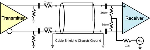
The characteristic impedance of both cables and the backplane implementation is 100 Ohms differential (nominal).
LVDS Eye Diagram
Jitter, Noise, and Signal Attentuation
As the bit stream travels from the transmitter on one end of a link to the receiver on the other end, it is subject to the following disruptive influences:
Deterministic (i.e., predictable) jitter induced by the cable and the connectors.
Data-dependent jitter induced by the dynamic data patterns on the wire.
Noise induced into the signal pair.
Signal attentuation.
The Eye Test
Refer to Figure 26-5 on page 689. In order to ensure that the differential receiver receives an in-specification signal, an eye test is performed. The following description of the eye diagram was provided by James Edwards from an article he authored for OE Magazine. The author of this book has added some additional comments [in brackets).
Figure 26-5. LVDS (Low-Voltage Differential Signal) Eye Diagram
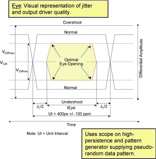
“The most common time domain measurement for a transmission system is the eye diagram. The eye diagram is a plot of data points repetitively sampled from a pseudo-random bit sequence and displayed by an oscilloscope. The time window of observation is two data periods wide. For an [InfiniBand link running at 2.5Gb/s], the period is 400ps, and the time window is set to 800 ps. The oscilloscope sweep is triggered by every data clock pulse. An eye diagram allows the user to observe system performance on a single plot.
To observe every possible data combination, the oscilloscope must operate like a multiple-exposure camera. The digital oscilloscope's display persistence is set to infinite. With each clock trigger, a new waveform is measured and overlaid upon all previous measured waveforms. To enhance the interpretation of the composite image, digital oscilloscopes can assign different colors to convey information on the number of occurrences of the waveforms that occupy the same pixel on the display, a process known as color-grading. Modern digital sampling oscilloscopes include the ability to make a large number of automated measurements to fully characterize the various eye parameters. ”
The oscilloscope is set for infinite-persistence and a pattern generator is set up to generate a pseudo-random data pattern.
Optimal Eye
The most ideal reading would paint an eye pattern such as that shown in the center of the figure (labelled “Optimal Eye Opening”). It should be noted, however, that as long as the pattern painted resides totally within the region noted as “Normal,” the transmitter, connectors, and cable are within tolerance.
Jitter Widens the Eye
Refer to Figure 26-6 on page 690. Jitter will cause a clock pulse to occur either before or after the “Optimal Eye Opening” resulting in an eye opening wider than the optimal width. Once again, as long as the amount of jitter doesn't cause the window to widen beyond the normal zone, it is still within tolerance.
Figure 26-6. Eye Diagram Jitter Indication

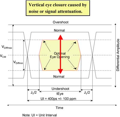
Noise and Signal Attenuation Heighten the Eye
Refer to Figure 26-7 on page 691. Noise or signal attenuation will cause the signal's voltage level to overshoot or undershoot the “Optimal Eye Opening” zone. As long as the amount of undershoot or overshoot doesn't cause the window height to dip below or extend above the normal zone, it is still within tolerance.
Figure 26-7. Eye Diagram Noise/Attenuation Indication
Output Driver Characteristics
Table 26-1 on this page lists the output driver characteristics.
Input Receiver Characteristics
Table 26-2 on this page lists the input receiver characteristics.
| Item | Max. | Min. | Units | Notes |
|---|---|---|---|---|
| VCM | 1.0 | 0.5 | V | Common mode voltage |
| Vdiff | 1.6 | 1.0 | V | Differential voltage |
| Vstandby | 1.6 | 0 | V | Quiescent (Sleeping State) |
| Vdisable | 1.6 | 0 | V | Quiescent (Disabled State) |
| tDRF | 100 | ps | Rise/fall time (20%–80%) | |
| SDBtB | 500 | ps | Lane-to-lane skew | |
| VacCM | 25 | mV | AC common mode noise | |
| IacCM | 5 | uA | AC common mode noise | |
| JT | 140 | ps | Jitter at output pin | |
| tEye | 260 | ps | Minimum eye opening | |
| ZD | 125 | 75 | Ohm | Differential impedance |
| Item | Max. | Min. | Units | Notes |
|---|---|---|---|---|
| VCM[*] | 1.25 | 0.25 | V | Common Mode |
| Vdiff | 1.6 | 0.175 | V | A signal less than 0.085V is considered absent. |
| Vtt [*] | 1.0 | 0.5 | ||
| tDRF | 100 | ps | Rise/Fall time (20%–80%) | |
| SRBtB | 24 | ps | Receiver lane-to-lane skew | |
| JT | 260 | ps | Jitter at input pin | |
| tEye | 140 | ps | Minimum eye opening | |
| ZD | 125 | 75 | Ohm | Differential impedance |
| ZVtt | 30 | Ohm | ||
| Zrterm | 62.5 | 40 | Ohm | Differential impedance |
[*] Note: Unless DC block capacitors are present at receiver.
Connector Operational Characteristics
The mechanical definitions for plugs and connectors are clearly defined in the specification and are not reproduced here. Table 26-3 on this page lists the operational characteristics of the electrical connector.
| Connector Parameter | Max. | Min. | Units |
|---|---|---|---|
| Differential Impedance | 110 | 90 | Ohm |
| Current Rating | 0.5 | A | |
| Within Pair Skew | 5 | ps | |
| Jitter | 10 | ps |
Copper Cable Operational Characteristics
The specification does not specify a particular type of cable, nor does it specify the bulk wire conductor size, insulation type, and so forth. Each of the two conductor pairs are twisted and shielded (the shield is connected to IB_Sh_Ret, which is connected to board signal ground—see Figure 26-1 on page 684 and Figure 26-2 on page 685), and both are encased in the outer bulk shield, which is connected to the chassis ground at both ends. Each cable signal pair connects from the transmit signal pair at the source to the receiver pair at the destination port.
Table 26-4 on this page lists the operational characteristics of the copper cable.
| Connector Parameter | Max. | Min. | Units |
|---|---|---|---|
| Differential Impedance | 155 | 95 | Ohm |
| Pair-to-Pair Skew | 50 | ps/m | |
| Within Pair Skew | 120 | ps | |
| Jitter | 100 | ps |