
Chapter 3: Hardware architecture
Abstract
This chapter explains the hardware architecture of the Huawei Ascend AI Processor. Firstly, the main components of the System on Chip (SoC) are introduced, including Control CPU, AI Core, AI CPU, Cache/Buffer, and Digital Vision Preprocessing (DVPP) module. The main part of AI computation is AI Core, which is designed following Huawei’s DaVinci architecture. In this chapter, the DaVinci architecture is explained in detail, covering its computing unit, memory system, control units, and instruction set design. At the end of the chapter, it is explained in detail how convolution operation is accelerated in the Ascend AI processor. A comparison between different AI processor architectures is also provided.
Keywords
Hardware architecture; System on chip; SoC; Digital vision preprocessing; DVPP; DaVinci architecture
In order to meet the increasing demands on the computing power of deep neural networks, Huawei launched the Ascend AI processor series in 2018 [1]. The Ascend AI processor provides powerful and highly efficient computing power for integer- and floating-point multiplication and addition operations. The Ascend AI processors not only have a large computational capacity, but also implement many special optimizations at the level of hardware architecture, which achieves high efficiency in performing forward computation of current mainstream deep neural networks. Therefore, it has great potential for various smart device applications.
3.1: Hardware architecture overview
The Ascend AI processor is a System on Chip (SoC) [2], as shown in Fig. 3.1. It can be used in many applications such as image, video, voice, and language processing. Its main architectural components include special computing units, large-capacity storage units, and the corresponding control units. The processor can be roughly divided into Control CPU, AI Computing Engine (including AI Core and AI CPU), multilevel on-chip system cache (Cache) or buffer (Buffer), Digital Vision Preprocessing module (DVPP), and etc. The processor adopts high-speed LPDDR4 [3] as the main memory controller interface which is more cost-effective than other alternatives. At present, the main memory of most SoC chips is generally composed of DDR (Double Data Rate) or HBM (High Bandwidth Memory) [4] to store large data. HBM has a higher storage bandwidth than DDR does, and it is the trend in the storage industry. Other common peripheral interface modules include USB, disk, network card, GPIO [5], I2C [6], power management interfaces, and so on.
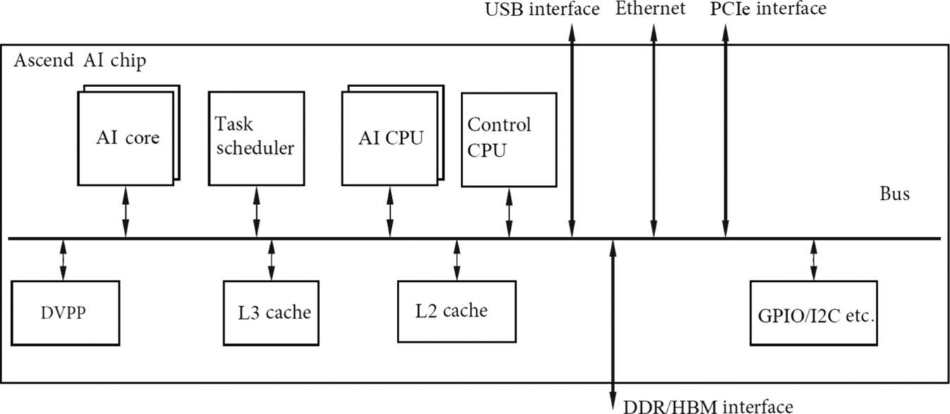
When Ascend AI processors are used to accelerate servers, a PCIe interface [7] is used for data exchange between the processors and other hardware units. All of the above units are connected by an on-chip ring bus based on the CHI protocol, which defines the data exchange mechanism among modules and ensures data sharing and consistency.
The Ascend AI processor integrates multiple ARM CPU cores, each of them has its own L1 and L2 caches with all CPUs sharing an on-chip L3 cache. The integrated CPUs can be divided into the main CPU that controls the overall system and AI CPUs for nonmatrix complex calculations. The number of cores of CPUs can be allocated dynamically through software based on the immediate requirements.
Besides CPUs, the main computing power of Ascend AI processors is achieved by AI Core, which uses the DaVinci hardware architecture. These AI Cores, through specially designed hardware architectures and circuits, can achieve high throughput, high computational power, and low power consumption. They are especially suitable for matrix multiplications, the essential computation for neural networks in deep learning. At present, the processor can provide powerful multiplication and addition computations for integer-type (INT8 and INT4) or floating-point numbers (FP16). Taking advantage of modular design allows further increases to computational power by incorporating various modules.
In order to store and process large amounts of parameters needed by deep networks and intermediate temporary results, the processor also equips the AI computing engine with an 8 MB on-processor buffer to provide high bandwidth, low latency, and high-efficiency data exchange. The ability to quickly access needed data is critical to improving the overall running performance of the neural network. Buffering a large amount of intermediate data to be accessed later is also significant for reducing overall system power consumption. In order to achieve efficient allocation and scheduling of computing tasks on the AI Core, a dedicated CPU is used as a Task Scheduler (TS). This CPU is dedicated to scheduling tasks between AI Core and AI CPUs only.
The DVPP module is mainly in charge of the image/video encoding and decoding tasks. It supports 4 Ka resolution video processing and image compressions such as JPEG and PNG. The video and image data, either from host memory or network, need to be converted to meet processing requirements (input formats, resolutions, etc.) before entering the computing engine of the Ascend AI processor. The DVPP module is called to convert format and precision accordingly. The main functionality of Digital Vision Preprocessing Module includes video decoding (Video Decoder, VDEC), video encoding (Video Encoder, VENC), JPEG encoding and decoding (JPEG Decoder/Encoder, JPEGD/E), PNG decoding (PNGD) and vision preprocessing (Vision Preprocessing Core, VPC), etc. Image preprocessing can perform various tasks such as up/downsampling, cropping, and color conversion. The DVPP module uses dedicated circuits to achieve highly efficient image processing functions, and for each function, a corresponding hardware circuit module is designed to implement it. When the DVPP module receives an image/video processing task, it reads the image/video data and distributes it to the corresponding processing module for processing. After the processing completes, the data is written back to memory for the subsequent processing steps.
3.2: DaVinci architecture
Unlike traditional CPUs and GPUs that support general-purpose computing, or ASIC processors dedicated to a particular algorithm, the DaVinci architecture is designed to adapt to common applications and algorithms within a particular field, commonly referred to as “domain-specific architecture (DSA)” processors.
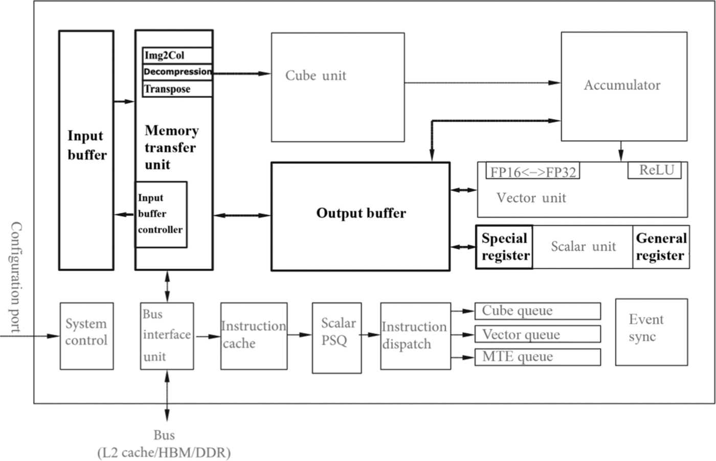
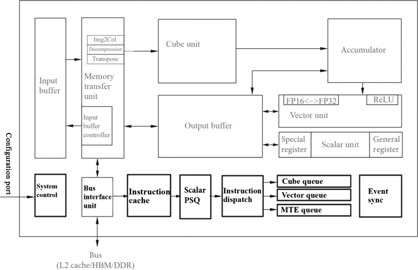
AI Core is the main computing core in Ascend AI processor, which is responsible for executing scalar, vector, and tensor-related computation-intensive operations. AI Core adopts the DaVinci architecture, whose basic structure is shown in Fig. 3.2. It can be seen as a relatively simplified basic architecture of modern microprocessors from the control point of view. It includes three basic computing resources: Cube Unit, Vector Unit, and Scalar Unit. These three computing units correspond to three common computing modes: tensor, vector, and scalar. In the process of computation, each unit performs its own duties, forming three independent execution pipelines, which cooperate with each other under the unified scheduling of system software to achieve optimal computing efficiency. In addition, different calculation modes are designed with different precision requirements in Cube and Vector units. Cube Unit in AI Core can support the calculation of INT8, INT4, and FP16; and Vector Unit can support the calculation of FP16 and FP32 at the moment.
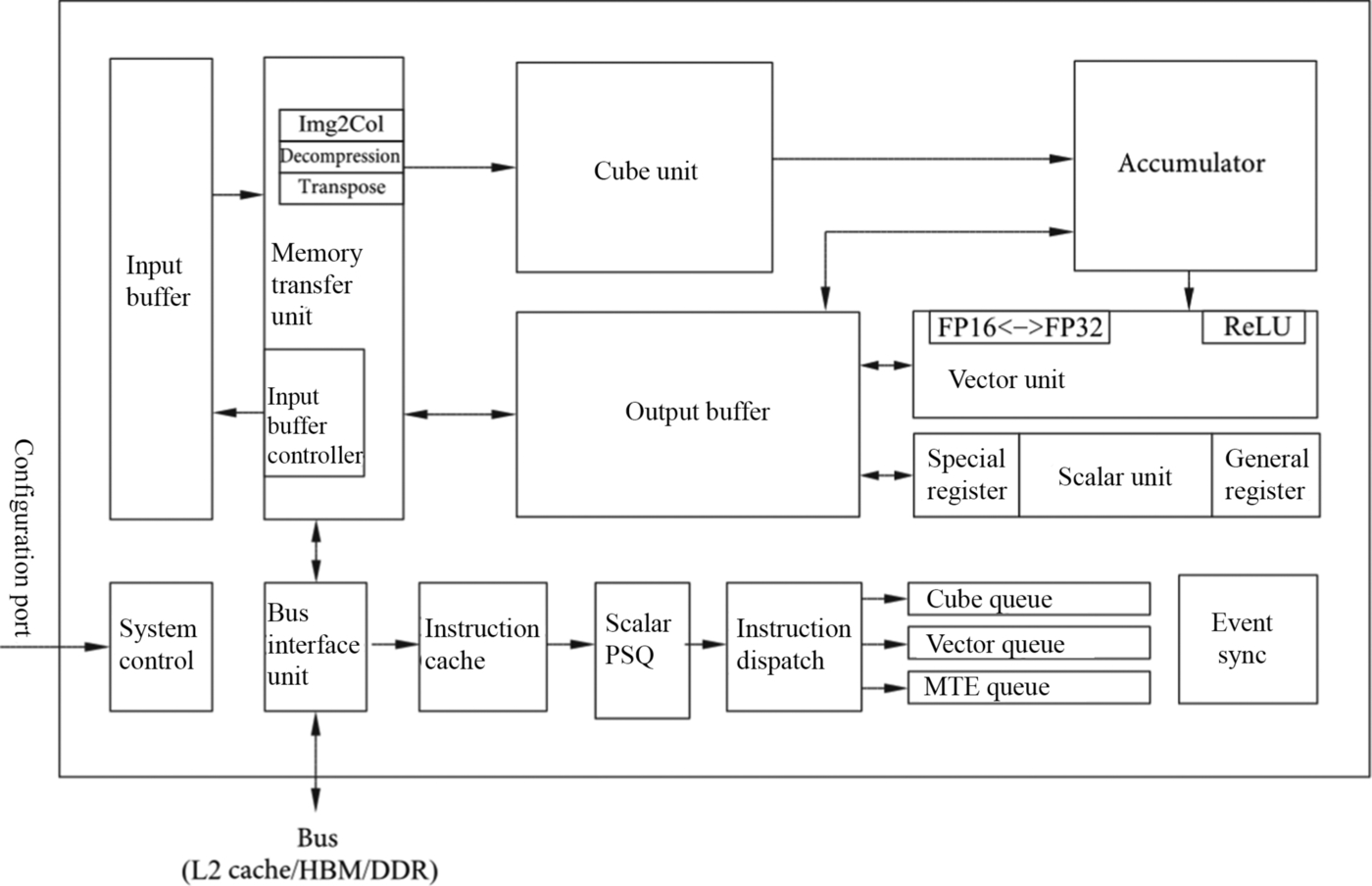
In order to coordinate the data transmission of AI Core, a series of on-chip buffers are distributed around three kinds of computing units. These on-chip buffers, e.g., Input Buffer (IB) and Output Buffer (OB), are used to store the entire image features, model parameters intermediate results, and so on. These buffers also provide high-speed register units that can be used to store temporary variables in the computing units. Although the design architectures and organization of these storage resources are different, they serve the same goal, i.e., to better meet the different input formats requirements, accuracy, and data layout for different computing modes. These storage resources are either directly connected to the associated computing hardware resources or to the bus interface unit (BIU) to obtain data on the external bus.
In AI Core, a memory transfer unit (MTE) is set up after the IB, which is one of the unique features of DaVinci architecture, the main purpose is to achieve data format conversion efficiently. For example, as mentioned earlier, GPU needs to apply convolution by matrix computation. It first needs to arrange the input network and feature data in a certain format through Img2Col. This step in GPU is implemented in software, which is inefficient. DaVinci architecture uses a dedicated memory conversion unit to process this step, which is a monolithic hardware circuit and so can complete the entire conversion process quickly. The customized circuit modules for transpose operation, one of the frequent operations in a typical deep neural network, can improve the execution efficiency of AI Core and achieve uninterrupted convolution operations.
The control unit in AI Core mainly includes System Control, Scalar PSQ, Instruction Dispatch, Matrix Queue, Vector Queue, Memory Transfer Queue, and Event Sync. The system control is responsible for commanding and coordinating the overall operation of AI Core, configuring parameters, and doing power control. Scalar PSQ mainly implements the decoding of control instructions. When instructions are decoded and sent out sequentially through Instruction Dispatch, they are sent to Matrix Queue, Vector Queue, and Memory Transfer Queue according to the types of instructions. The instructions in the three queues are independently given to the Cube Unit, the Vector Unit, and the MTE according to a first-in-first-out (FIFO) mechanism. Since different instruction arrays and computing resources construct independent pipelines, they can be executed in parallel to improve instruction execution efficiency. If there are dependencies or mandatory time sequence requirements during instruction execution, the order of instruction execution can be adjusted and maintained by Event Sync. Event Sync is entirely controlled by software. In the process of coding, the execution sequence of each pipeline can be specified synchronizer symbols, to adjust the execution sequence of instructions.
In AI Core, the Memory Unit provides transposed data which satisfies the input format requirements for each computing unit, the computing unit returns the result of the operation to the Memory Unit, and the control unit provides instruction control for the various computing units and the Memory Unit. The three units coordinate together to complete the computation task.
3.2.1: Computing unit
Computing Unit is the core unit of AI Core, which provides powerful computing power, it is the main force of AI Core. AI Core computing units mainly include the Cube Unit, Vector Unit, Scalar Unit, and accumulator, as shown in Fig. 3.3. Cube Unit and accumulator mainly complete matrix-related operations, Vector Unit is responsible for vector operations, and Scalar Unit is mainly responsible for all types of scalar data operations and program control flow.
3.2.1.1: Cube unit
- (1) Matrix multiplication
Due to the extensive use of matrix computing in the common deep neural network, the DaVinci architecture specifically optimizes matrix computing in-depth and customizes Cube Units to support high-throughput matrix operations. Fig. 3.4 shows the multiplication operation C = A × B between matrix A and B, where M represents the number of rows of matrix A, K represents the number of columns of matrix A and the number of rows of matrix B, and N represents the number of columns of matrix B. The matrix multiplication computation in a traditional CPU is shown in Code 3.1.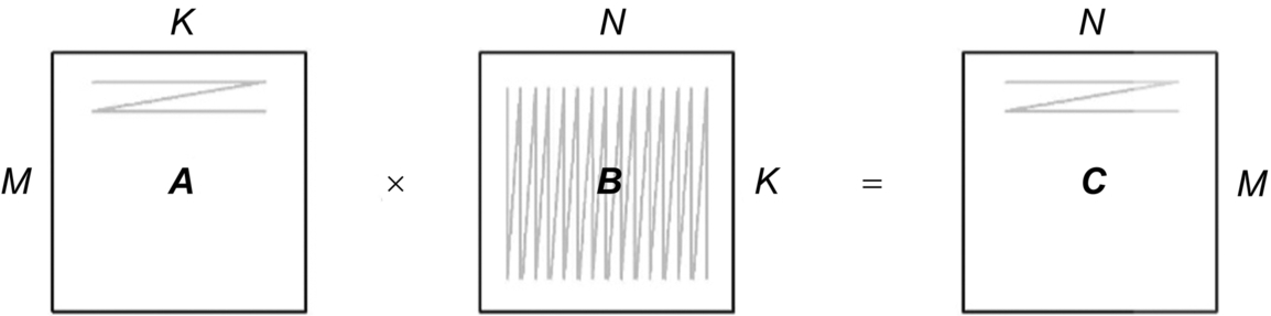
Fig. 3.4 Matrix multiplication illustration.
This program needs three loops to perform a complete matrix multiplication calculation. If it is executed on a single instruction dispatch CPU, it needs at least M × K × N clock cycles to complete the operation. When the matrix is very large, the execution process is extremely time consuming.
In the computation process using CPU, matrix A is scanned row-by-row and matrix B is scanned column-by-column. Considering how a matrix is typically stored in the memory, both matrix A and matrix B are stored row-by-row, so-called row-major mode. Memory accessing often has strong patterns. For example, when reading a number in a matrix into memory, it puts a whole line in memory and reads all the numbers of the same line together. This method of memory reading is very efficient for matrix A, but very inefficient for matrix B because matrix B in the code needs to be read column by column. In this case, it is beneficial to convert the storage mode of matrix B into column-by-column storage, so-called Column-Major (Fig. 3.5) mode, so as to conform to the efficient memory reading. The efficiency of matrix computing is often improved by changing the storage mode of a relevant matrix.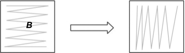
Fig. 3.5 Matrix B storage mode.
Generally speaking, when the matrix is large, due to the limitations of computing and memory on the processor, it is often necessary to split the matrix (Tiling), as shown in Fig. 3.6. Due to the capacity of on-chip cache, when it is difficult to load the whole matrix B at one time, matrix B can be divided into several submatrices such as B0, B1, B2, and B3. Each submatrix can be stored in a cache on the processor to calculate with matrix A to get the result submatrix. The purpose of this method is to fully utilize the data locality principle, reuse the submatrix data in the cache as much as possible to get all relevant submatrix results, then read the new submatrix for the next cycle. In this way, all the submatrices can be moved to the cache one by one, and the whole process of matrix calculation can be completed efficiently. Finally, the resulting matrix C can be obtained. As one of the common optimization methods for matrix computation, the advantage of partitioning is that it makes full use of caching capacity and maximizes the use of data locality in the process of computation. This allows it to achieve high efficiency especially for large-scale matrix multiplication computations.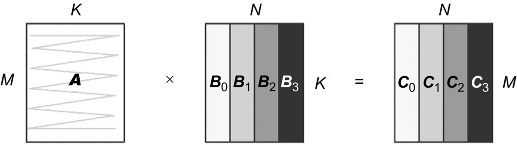
Fig. 3.6 Matrix operation using tiling. - (2) Computing method of cube unit
To implement the convolution process in deep neural networks, the key step is to convert the convolution operation into matrix operation. Large matrix computation in CPUs often becomes a performance bottleneck, however, such computations are crucial for deep learning. In order to solve this dilemma, GPUs use General Matrix Multiplication (GEMM) to implement matrix multiplications. For example, to multiply a 16 × 16 matrix with another 16 × 16 matrix, 256 parallel threads are used, and each thread can calculate one output point in the resulting matrix independently. Assuming that each thread can complete a multiplication and addition operation in one clock cycle, the GPU needs 16 clock cycles to complete the whole matrix calculation. This delay is an inevitable bottleneck for GPU. The Ascend AI processor has made further optimizations to avoid this bottleneck. The high efficiency of AI Core for matrix multiplication guarantees high performance for the Ascend AI processor when used as an accelerator for deep neural networks.
In AI Core, DaVinci architecture specially designed a Cube Unit as the core computing module of Ascend AI processor, aiming at removing the bottleneck of matrix computations. Cube Unit (CU) provides powerful parallel multiplication and addition computations, enabling AI Core to finish matrix computations rapidly. Through the elaborate design of customized circuits and aggressive back-end optimizations, the Cube Unit can complete the multiplication operation of two 16 × 16 matrices with one instruction (referred to as 163, also the name origin of Cube). This corresponds to 163 = 4096 multiplication and addition operations with FP16 precision in a single instruction. As shown in Fig. 3.7, to compute matrix operation of A × B = C, the Cube Unit stores matrix A and B in the IB, and after computation, the result matrix C is stored in the OB. In matrix multiplication (Fig. 3.7), the first element of matrix C is obtained through 16 multiplications and 15 additions (using Cube Unit subcircuits) on 16 elements in the first row of A and 16 elements in the first column of B. There are 256 matrix computing subcircuits in the Cube Unit, which can calculate 256 elements of matrix C in parallel using only one instruction.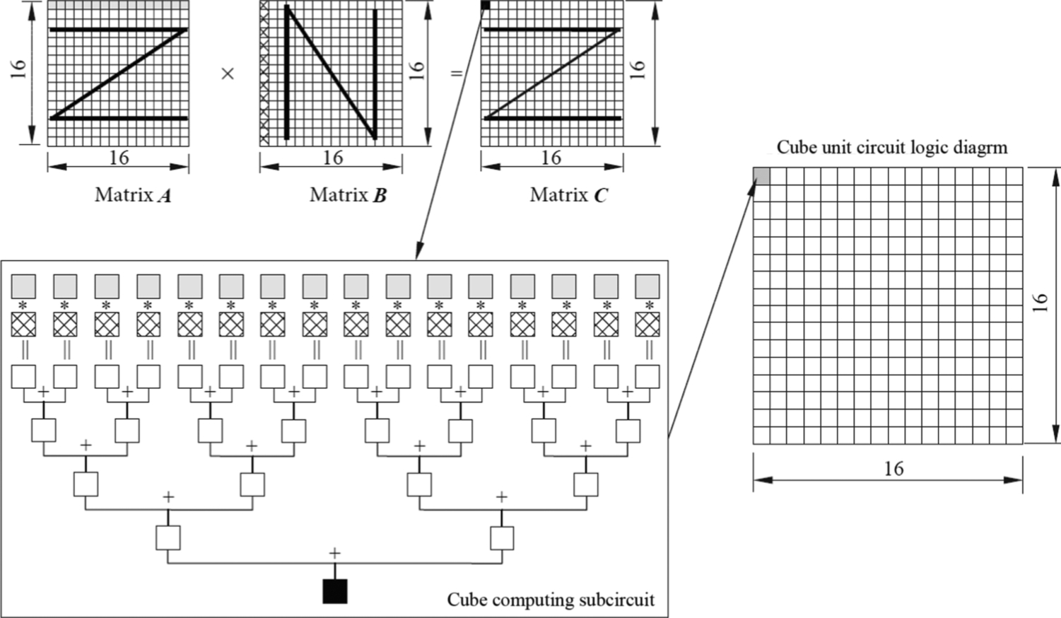
Fig. 3.7 Cube unit calculation illustration.
In matrix computations, it is very common to accumulate the result of one matrix multiplication with itself such as C = A × B + C. The design of the Cube Unit also takes this situation into account. A group of accumulator units is added after the Cube Unit, which can accumulate the last intermediate results with the current results. The total number of accumulations can be controlled by software, and the final results can be written to the output after the accumulation is completed. For convolution operations, the accumulator can be used to complete the addition of the bias term.
Cube Unit can quickly accomplish matrix multiplication of 16 × 16. However, when a matrix is larger than 16 × 16, it needs to be stored in a specific format in advance and read in a specific block-splitting way during the step of the computation. As shown in Fig. 3.8, the partitioning and sorting method shown as A is called “big Z and small Z.” It is intuitive to see that each block of A is sorted according to the index order of rows, and it is called “big Z.” The data of each internal block is also arranged row-by-row, which is called as “small Z.” Each block of matrix B is sorted by rows, while the inner part of each block is sorted by columns, which is called the “big Z small N” partitioning method. According to the general rule of matrix calculation, the resulting matrix C obtained by multiplying the A and B matrices, which is arranged as each block matrix being partitioned by columns, and the data inside each block being partitioned by row, so-called “big N and small Z” arrangement.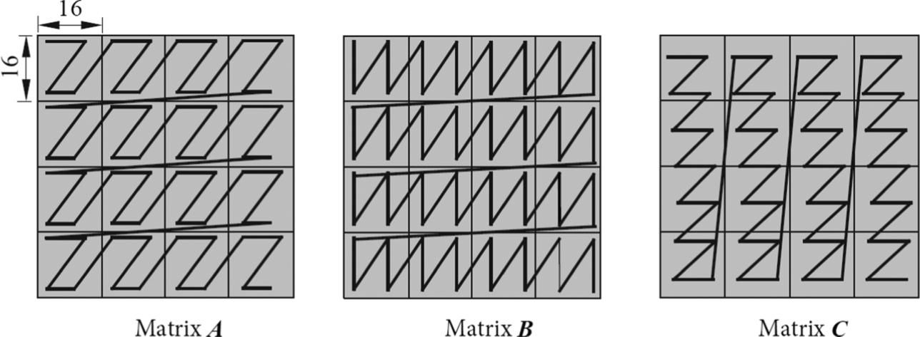
Fig. 3.8 Data storage format requirement.
When using the Cube Unit to compute large-scale matrices, due to the memory limitation, it is impossible to store the entire matrix at once. Therefore, it is necessary to partition the matrix and perform the calculation step-by-step. Fig. 3.9 shows the matrix A and matrix B are equally divided into blocks of the same size, as 16 × 16 submatrixes. During partitioning, the missing row/columns are padded with zeros. At first, obtain the resulting submatrix C1, which needs to be calculated in two steps: the first step moves A1 and B1 to the Cube Unit and calculates the intermediate result of A1 × B1. At the second step, moves A2 and B2 to the Cube Unit and calculate A2 × B2. After that, accumulate these two results to get the final submatrix C1, then C1 is written into the output buffer. Since the output buffer capacity is also limited, it is necessary to write the C1 submatrix into the memory as soon as possible, in order to leave spaces for the next result, e.g., submatrix C2. By repeating the same mechanisms, the computation of the entire large-scale matrix multiplication can be achieved efficiently.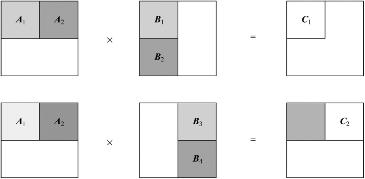
Fig. 3.9 Matrix computation using partitions.
In addition to FP16-type operations, the Cube Unit can also support lower precision types such as INT8. For INT8, the Cube Unit can perform a matrix multiplication operation of 16 × 32 or 32 × 16 at once. By adjusting the precision of the Cube Unit accordingly to the computation requirement of deep neural networks, it is possible to achieve better performance.
Along with FP16 and INT8 operations, the Cube Unit also supports UINT8, INT4, and U2 data types. In terms of U2 data type, only the two-bit weight (U2 Weight) calculation is supported. Due to the popularity of the lightweight neural network using two-bit weights, U2 weight data will be converted into FP16 or INT8 for computations.
3.2.1.2: Vector unit
The Vector Unit in AI Core is mainly responsible for performing vector-related operations. It supports computations for one vector, computations between one vector and scalar, and computations between two vectors. All the computations support various data types, such as FP32, FP16, INT32, and INT8.
Fig. 3.10 shows the Vector Unit can quickly complete two FP16 type vector computations. Note that both the input and output data of the Vector Unit are usually stored in the OB (Fig. 3.2). For Vector Units, the input data can be stored in discontinuous memory space, depending on the addressing mode of the input data. The addressing mode supported by Vector Unit includes continuous addressing mode and fixed interval addressing mode. In special cases where vectors having irregular addresses, the Vector Unit also provides vector address registers to be used for addressing those vectors.
As shown in Fig. 3.2, the Vector Unit could serve as a data bridge between the Cube Unit and the output buffer. In the process of transferring the result of matrix computation to the output buffer, the Vector Unit can conveniently complete some common computations of deep neural networks, especially in convolutional neural networks, such as the activation functions (ReLU [8]) and various pooling functions, etc. The Vector Unit can also perform data format conversion before the data are written back to the OB or Cube Unit for the next operation. All these operations can be implemented by software with corresponding Vector Unit instructions. Vector Unit provides abundant basic computations together with many special vector computations to complement the matrix computations of the Cube Unit and provides AI Core with comprehensive computation for nonmatrix data.
3.2.1.3: Scalar unit
Scalar Unit is responsible for scalar-related computations in AI Core. It also behaves like a mini-CPU that controls the entire AI Core. Scalar Unit can control the iterations in programs and recognize conditional statements. It can also control how other modules are executed in the AI Core pipeline by inserting synchronizer in the Event Sync module. In addition, it calculates the address of data and related parameters to support the Cube Unit or Vector Unit. Furthermore, it provides many basic arithmetic operations. Note that other highly complex scalar operations are fulfilled by the AI CPU with customized operators.
There are several general purpose registers (GPR) and special purpose registers (SPR) around the Scalar Unit. GPRs can be used to store variables or addresses, providing input data for arithmetic logic operations and storing intermediate computation results. SPRs are designed to support the special functionality of specific instructions in the instruction set. Generally, they cannot be accessed directly, only part of SPR can be read and written by special instructions.
The SPRs in AI Core include CoreID (used to identify different AI Core), VA (vector address register), and STATUS (AI Core run state register), and so on. Programmers can control and change the running state and mode of AI Core by monitoring these special registers.
3.2.2: Memory system
The Ascend AI processor memory system includes two parts: (1) on-chip memory unit, (2) the corresponding data transfer bus. It is well known that almost all deep learning algorithms are data intensive. Therefore, a well-designed data memory and transfer structure are crucial to the performance of Ascend AI processors. The suboptimal design generally creates performance bottlenecks, which could waste other resources in the processor. Through optimization and coordination among various types of distributed buffers, AI Core provides very fast data transfer for the deep neural network. It eliminates the bottleneck of data transmission to improve overall computing performance and to support efficient extraction and transfer of large-scale, concurrent data required in deep learning neural networks.
3.2.2.1: Memory unit
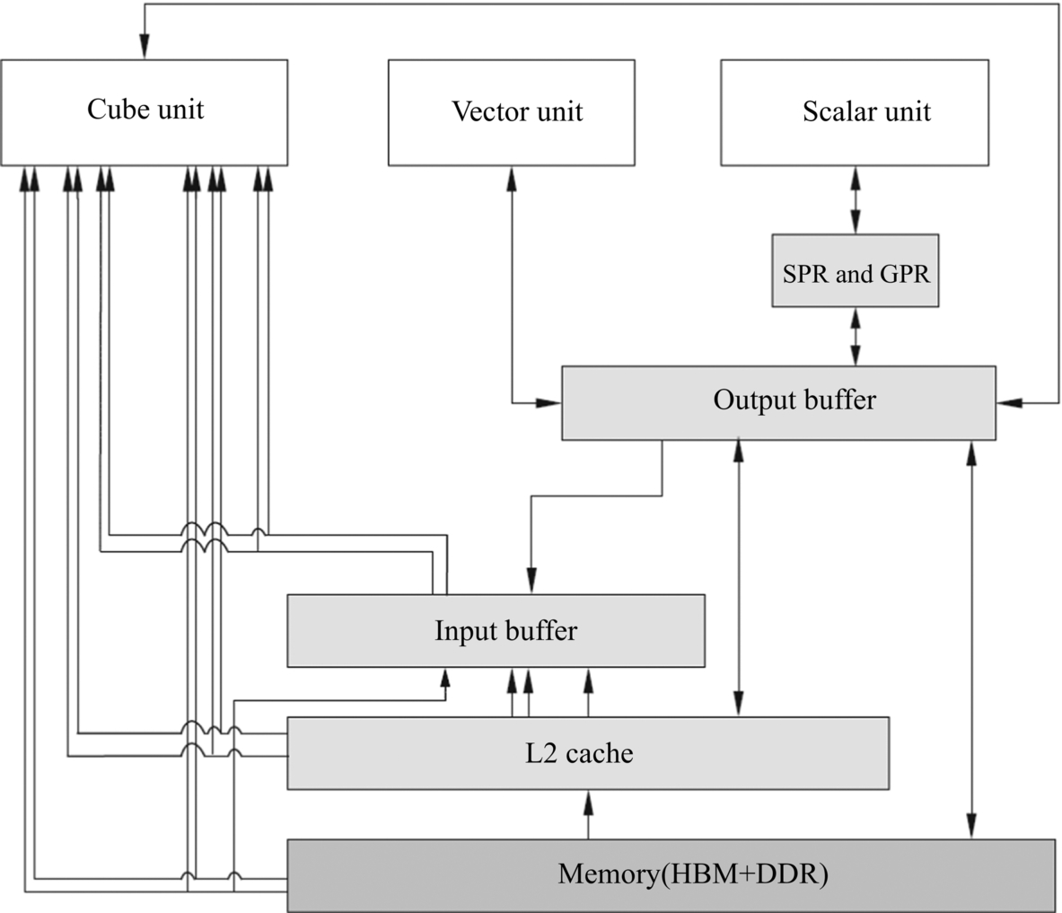
To achieve optimal computing power in the processor, it is essential to ensure that the input data can be fed into the computing unit rapidly and without corruption. The DaVinci architecture ensures accurate and efficient data transfer among computing resources through well-designed memory units which are the logistics system in AI Core. The memory units in AI Core is composed of Memory Control Units, Buffers, and Registers (bold in Fig. 3.11). Memory Control Unit can directly access lower-level caches outside AI Core through the data bus interface and can also access memory directly through DDR or HBM. The MTE is also set up in the memory control unit, which aims at converting the input data into data formats compatible with various types of computing units in AI Core. Buffers include IBs that temporarily store the input image feature maps and OBs which are placed in the center of the processor can temporarily store various forms of intermediate and final outputs. The various registers in AI Core are mainly used by Scalar Unit.
Read and write operations of all buffers and registers can be explicitly controlled by the underlying software. Experienced programmers can use advanced programming techniques to avoid read and write conflicts that affect the performance of the pipeline. For regular neural network computations such as convolution or matrix operations, the corresponding programs can realize the whole process without blocking the execution of the pipeline.
The Bus Interface Unit in Fig. 3.11, as the “gate” of AI Core, is a bridge that connects the system bus and the external world. AI Core reads/writes data from/to the external L2 buffer, DDR, or HBM through the bus interface. In this process, the Bus Interface Unit can convert the read and write requests from AI Core to the external read and write requests that meet the bus requirements and complete the transaction and conversion using the predefined protocol.
The input data is read from the bus interface and processed by the MTE. As the data transmission controller of AI Core, the MTE is responsible for managing the internal data read and write operations among different buffers inside the AI Core. It includes tasks such as format conversion operations, zero-filling, Img2Col, transpose, and decompression, etc. The MTE can also configure the IB in AI Core to achieve local data caching.
For a deep neural network, the input image feature normally has a large number of channels and the input data volume is huge as well. The IB is often used to temporarily store the data that requires frequent reuse, in order to reduce power consumption and improve overall performance. When temporarily stored in the IB, the frequently used data does not need to be fed into the AI Core through the bus interface every time. It reduces data access frequency and the risk of congestion on the bus. This is important when data format conversion operation is carried out by the MTE. The DaVinci architecture stores the source data in the IB first, then it is possible to process data conversion. The entire data flow is controlled by the IB Controller. Storing in the IB makes it more efficient to move a large amount of data into AI Core at one time. This allows the data format to be converted rapidly using customized hardware eliminating performance bottlenecks that would otherwise be caused.
In the neural network, intermediate results of each layer can be placed in the OB, so that the data is easily obtained when processing the following layer. Using the OB greatly improves the computational efficiency when compared to reading data through the system bus which has low bandwidth and high latency.
The Cube Unit also contains a Supply Register which directly stores two input matrices of a 16 × 16 matrix multiplication. After the result is calculated, the accumulator caches the result matrix using a Result Register. With the help of the accumulator, the results of previous matrix calculation can be accumulated continuously, which is very common in running convolutional neural networks. The results in the Result Register can be transferred to the OB only once when all required cumulative operations complete, which can be controlled using software API.
Since the Memory System in AI Core provides continuous data flow, it fully supports the computing units to achieve high computing power. Therefore, it improves the overall computing performance of AI Core. This is similar to the Unified Buffer (UB) concept in Google’s TPU design, and AI Core uses a large-capacity on-chip buffer design to increase the on-chip cache volume, which further reduces the frequency of data transmission between off-chip storage and AI Core. This also helps reduce power consumption effectively to control the overall energy consumption of the entire system.
DaVinci Architecture uses customized circuits in the MTE to implement format conversion operations such as Img2Col, etc. These not only reduce power consumption but also save the instruction cost of data conversion. Such instructions, which can do data format conversion while transmitting, are called accompanying instructions. The hardware support of accompanying instructions is beneficial since it doesn’t need to schedule the conversion and transmission processes.
3.2.2.2: Data flow
Data flow refers to the data flowing path in AI Core when AI Core executes a computational task. The data flow path was briefly introduced in the previous section using matrix multiplication as an example. Fig. 3.12 shows the complete data flow within an AI Core in the DaVinci architecture. This includes DDR or HBM, as well as L2 caches, which belong to data storage systems outside the AI Core. All other types of data buffers in the diagram belong to the core memory system.
Data in the off-chip storage system can be directly transferred to the Cube Unit using LOAD instructions, and the output results will be stored in the OB. In addition to being transferred directly to the Cube Unit, data can also be transmitted to the IB first through LOAD then to the Cube Unit later by other instructions. The advantage of the latter approach is that the available large IB of temporary data can be reused many times by Cube Units.
Cube Units and OB can transfer data to each other. Because of limited storage in the Cube Unit, some matrix operation output is written into the OB in order to provide enough space for subsequent computations. When the time comes, data in the OB can also be moved back to the Cube Unit as input for subsequent calculations. Moreover, there are separate bidirectional data transmission buses between the OB and the Vector Unit as well as the Scalar Unit and the off-chip storage system, respectively. For example, data in the OB can be written into the Scalar Unit through a dedicated register or a general register.
It is worth to note that all data in AI Core must pass through the OB before being written back to the external storage. For example, if image feature data in the IB output to system memory, it is processed by the Cube Unit first with the output stored in the OB and finally is sent to off-chip storage from the OB. There is no data transmission bus directly from the IB to the OB in AI Core. Therefore, by serving arbiter of AI Core data outflow, the OB controls and coordinates the output of all core data accordingly.
The data transmission bus in the DaVinci architecture is characterized as multiple-input and single-output (MISO). Data can be fed into AI Core directly from outside to any of the Cube Unit, IB, and OB through multiple data buses. The data sinking path is flexible because data can be fed into the AI Core using different data pipelines separately controlled by software. On the other hand, output data must pass through the OB before it can be transferred to the off-chip storage.
The design is based on the characteristics of deep neural network computations, where input data has a great variety such as weights, bias terms of convolution layers, or eigenvalues of multiple channels. In AI Core, data can be stored accordingly in different memory units based on their type and can be processed in parallel. This greatly improves the data inflow efficiency in order to satisfy the needs of intensive mathematical computations. The advantage of multiple input data buses in AI Core is that they facilitate continuous data transmission of the source data into AI Core with few restrictions. On the contrary, outputs of deep neural networks are relatively simple, often only feature maps stored as matrices. According to this characteristic of neural network output, a single output data path is designed. As a result, the output data is centrally managed, thus reducing the hardware control units for output data.
To summarize, the data buses among storage units and the MISO data transmission mechanism in DaVinci architecture are designed based on the thorough study of most mainstream convolutional deep learning networks. The design principle is to reduce processor cost, improve data mobility, increase computing performance, and decrease control complexity.
3.2.3: Control units
In the DaVinci architecture, the Control Unit provides instructions for the entire computation process and is considered to be the heart of AI Core. It is responsible for the overall processing of the entire AI Core and so plays a vital role. The main components of the Control Unit are System Control, Instruction Cache, Scalar PSQ, Instruction Dispatch, Cube Queue, Vector Queue, MTE Queue, and Event Sync, shown as bolded in Fig. 3.13.
In the process of instruction execution, the instructions can be prefetched in advance, and multiple instructions can be read into the cache at the same time to improve the efficiency. Multiple instructions enter the instruction cache of AI Core from system memory through the bus interface where they wait to be decoded and executed quickly and automatically by the hardware. After the instruction is decoded, it will be imported into the Scalar PSQ for address decoding and execution control. These instructions include matrix computing instructions, vector computing instructions, and memory transfer instructions. Before entering the Instruction Dispatch module, all instructions are processed sequentially as conventional scalar instructions. After the address and parameters of these instructions are decoded by Scalar PSQ, the Instruction Dispatch sends them to the corresponding execution queue according to their types, only scalar instructions reside in Scalar PSQ for subsequent execution, as shown in Fig. 3.13.
Instruction execution queues consist of Matrix Queue, Vector Queue, and Memory Transfer Queue. Matrix computing instructions enter the Matrix Queue, vector computing instructions enter the Vector Queue, and memory transfer instructions enter the Memory Transfer Queue, respectively. The instructions in the same instruction execution queue are executed in the order they are entered. Different instruction execution queues can be executed in parallel and through multiple instruction execution queues. Parallel execution improves overall instruction execution efficiency.
When the instruction in the instruction execution queue arrives at the head of the queue, it begins the execution process and is distributed to the corresponding execution unit. For example, the matrix computing instructions will be sent to the Cube Unit, and the memory transfer instructions will be sent to the MTE. Different execution units can calculate or process data in parallel according to the corresponding instructions. The instruction execution process in the instruction queue is defined as the instruction pipeline.
When there is data dependence between different instruction pipelines, DaVinci architecture uses Event Sync to coordinate the process of each pipeline to maintain the correct execution order. Event Sync monitors the execution status of each pipeline at all times and analyzes the dependencies between different pipelines in order to solve the problem of data dependence and synchronization. For example, if the current instruction in the Matrix Queue depends on the result of the Vector Unit, the Event Sync will suspend the execution process of Matrix Queue, requiring it to wait for the result of the Vector Unit. When the Vector Unit completes the computation and outputs the results, the Event Sync notifies the Matrix Queue that the data is ready and can continue to execute the remaining instructions. The Matrix Queue executes the current instruction only after receives notification from Event Sync. In the DaVinci architecture, both internal synchronization and interpipeline synchronization can be achieved through Event Sync using software control.
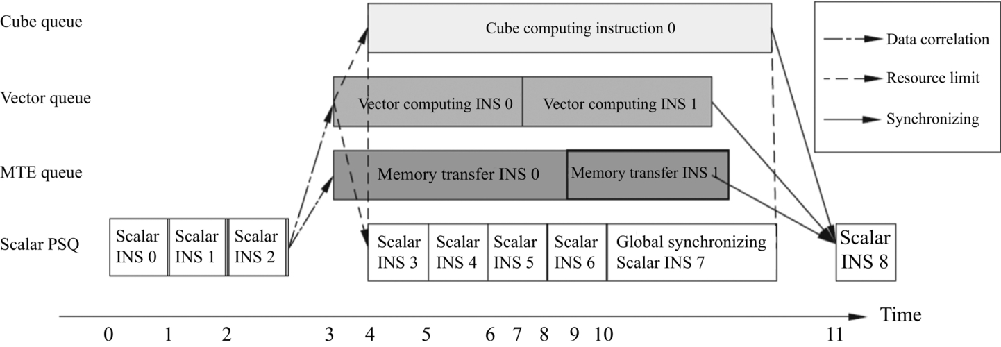
As shown in Fig. 3.14, the execution flow of four pipelines is illustrated. Scalar PSQ first executes scalar instructions S0, S1, and S2. Both the instruction V0 in Vector Queue and the instruction MT0 in Memory Transfer Queue have a dependency on S2. Therefore, they need to wait until S2 is completed before start execution. Because of these dependencies, the instructions have to be executed in sequential order. For the same reason, the matrix operation instructions M0 and scalar instructions S3 can only be executed at time 4. From time 4, the four instructions pipeline can be executed in parallel since all previous dependencies are resolved. The parallelization stops after scalar instruction S7 is executed in the Scalar PSQ. At this point, the Event Sync controls the matrix instruction pipeline, the vector instruction pipeline, and the memory transfer instruction pipeline in order to wait until the matrix operation instruction M0, the vector operation instruction V1, and the memory transfer instruction MT1 are all executed. After that, the scalar pipeline is allowed to continue executing scalar instruction S8.
There is also a System Control Module in the control units. Before AI Core runs, an external task scheduler is required to configure and initialize various interfaces of the AI Core, such as instruction configuration, parameter configuration, and task block configuration. One task block is defined as the smallest computational task that represents the task granularity in the AI Core. After the configuration is completed, the System Control Module will control the execution process of the task block. At the same time, after one task is completed, the System Control Module will process interrupts and report the status. If there is an error in the execution process, the System Control Module will report the execution error status to the task scheduler, which is merged into the current AI Core status information and finally exported to the Ascend AI processor top-level control system.
3.2.4: Instruction set design
When a program executes a computing task in the processor chip, it needs to be converted into a language that can be understood and processed by the hardware following a certain specification. Such language is referred to as the Instruction Set Architecture (ISA) or Instruction Set for short. The Instruction Set contains data types, basic operations, registers, addressing modes, data reading and writing modes, interruption, exception handling, and external I/O, etc. Each instruction describes a specific operation of the processor. An instruction set is a collection of all of the processor’s operations that can be invoked by a computer program. It is an abstract model of a processor’s functionality and an interface between computer software and hardware.
The instruction set can be classified into one of the Reduced Instruction Set Computer (RISC) and the Complex Instruction Set Computer (CISC). The advantages of simplified instruction sets include simple command functions, fast execution, and high compilation efficiency. However, simplified instruction sets cannot access the memory directly without using corresponding instructions. Common simplified instruction sets include ARM, MIPS, OpenRISC, and RISC-V, etc. [9]. On the other hand, in complex instruction sets, a single instruction is more powerful and supports more complex functionalities. And they support direct access to memory. However, it requires a longer command execution period. A common complex instruction set is x86.
There is a customized instruction set for the Ascend AI processor. The complexity of the instruction set in the Ascend AI processor is somewhere in between the simplified and complex instruction set. The instruction set includes scalar instructions, vector instructions, matrix instructions, and control instructions. A scalar instruction is similar to a simplified instruction set, while the matrix, vector, and data transfer instructions are similar to a complex instruction set. The Ascend AI processor instruction set combines the advantages of the simplified instruction set and complex instruction set, i.e., simple function, fast execution, and flexible memory access capability. Therefore, it is simple and efficient to transfer a large block of data.
3.2.4.1: Scalar instruction set
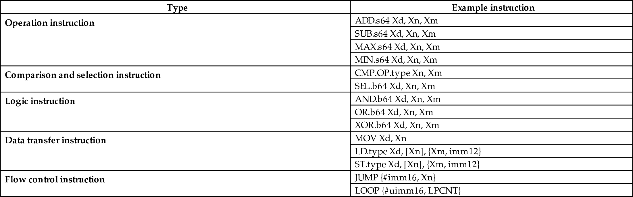
A scalar instruction is executed by a Scalar Unit and is mainly used to configure address and control registers for vector instructions and matrix instructions. It also controls the execution process of a program. Furthermore, the scalar instruction is responsible for saving and loading data in the OB and performing some simple data operations. Table 3.1 lists the common scalar instructions in the Ascend AI processor.
Table 3.1
| Type | Example instruction |
|---|---|
| Operation instruction | ADD.s64 Xd, Xn, Xm |
| SUB.s64 Xd, Xn, Xm | |
| MAX.s64 Xd, Xn, Xm | |
| MIN.s64 Xd, Xn, Xm | |
| Comparison and selection instruction | CMP.OP.type Xn, Xm |
| SEL.b64 Xd, Xn, Xm | |
| Logic instruction | AND.b64 Xd, Xn, Xm |
| OR.b64 Xd, Xn, Xm | |
| XOR.b64 Xd, Xn, Xm | |
| Data transfer instruction | MOV Xd, Xn |
| LD.type Xd, [Xn], {Xm, imm12} | |
| ST.type Xd, [Xn], {Xm, imm12} | |
| Flow control instruction | JUMP {#imm16, Xn} |
| LOOP {#uimm16, LPCNT} |
3.2.4.2: Vector instruction set
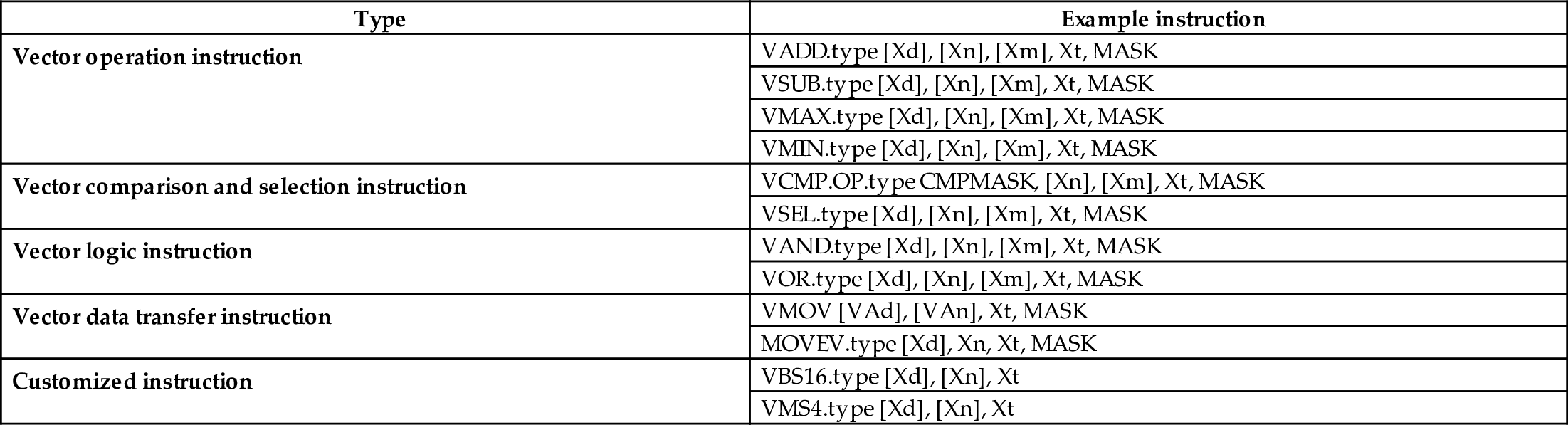
A vector instruction is executed by a Vector Unit, which is similar to a conventional Single Instruction Multiple Data (SIMD) instruction. Each vector instruction can perform the same type of operations on multiple samples. And the instruction can directly be run on the data in the OB without loading the data into the vector register with a data loading instruction. The data types supported are FP16, FP32, and INT32. The vector instruction supports recursive execution and the direct operation of vectors that are not stored in continuous memory space. Table 3.2 describes common vector instructions.
Table 3.2
| Type | Example instruction |
|---|---|
| Vector operation instruction | VADD.type [Xd], [Xn], [Xm], Xt, MASK |
| VSUB.type [Xd], [Xn], [Xm], Xt, MASK | |
| VMAX.type [Xd], [Xn], [Xm], Xt, MASK | |
| VMIN.type [Xd], [Xn], [Xm], Xt, MASK | |
| Vector comparison and selection instruction | VCMP.OP.type CMPMASK, [Xn], [Xm], Xt, MASK |
| VSEL.type [Xd], [Xn], [Xm], Xt, MASK | |
| Vector logic instruction | VAND.type [Xd], [Xn], [Xm], Xt, MASK |
| VOR.type [Xd], [Xn], [Xm], Xt, MASK | |
| Vector data transfer instruction | VMOV [VAd], [VAn], Xt, MASK |
| MOVEV.type [Xd], Xn, Xt, MASK | |
| Customized instruction | VBS16.type [Xd], [Xn], Xt |
| VMS4.type [Xd], [Xn], Xt |
3.2.4.3: Matrix instruction set
The matrix instruction is executed by the Matrix Calculation Unit to achieve efficient matrix multiplication and accumulation operations{C = A × B + C}. In the neural network computation process, a matrix A generally represents an input feature map, a matrix B generally represents a weight matrix, and a matrix C is an output feature map. The matrix instruction supports input data of INT8 and FP16 data types and supports computation for INT32, FP16, and FP32 data types. Currently, the most commonly used matrix instruction is the matrix multiplication and accumulation instruction MMAD:
MMAD.type [Xd], [Xn], [Xm], Xt
[Xn] and [Xm] are the start addresses of input matrix A and B, and [Xd] is the start address of output matrix C. Xt is a configuration register which consists of three parameters: M, K, and N, indicating the sizes of matrix A, B, and C, respectively. In matrix computation, the matrix multiplication and accumulation operation is performed using the MMAD instruction repeatedly, to accelerate the convolution computation of the neural network.
3.3: Convolution acceleration principle
In a deep neural network, convolution computation plays an important role. In a multilayer convolutional neural network, the convolution computation is often the most important factor that affects the performance of the system. The Ascend AI processor, as an artificial intelligence accelerator, puts more focus on convolution operations and optimizes the convolution calculation in both hardware and software architectures.
3.3.1: Convolution acceleration
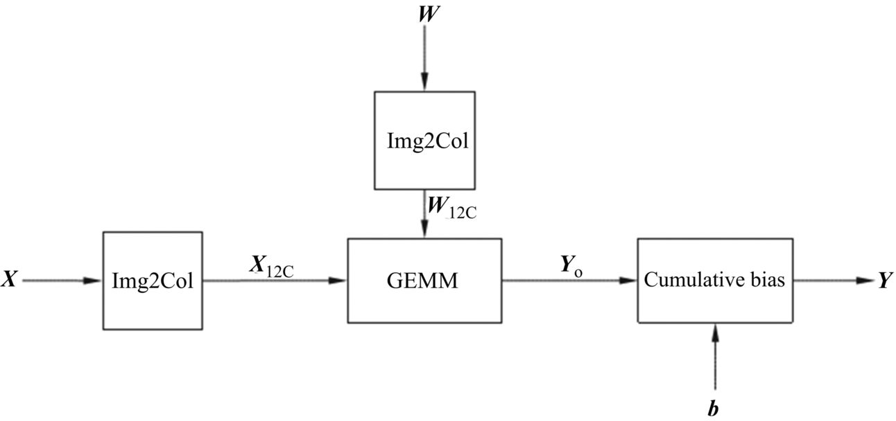
Fig. 3.15 shows a typical computation process of a convolution layer, where X is an input feature map, and W is a weight matrix; b is the bias values. Yo is the intermediate output. Y is the output feature map, and GEMM refers to the General Matrix Multiplication. Matrices X and W are first processed by Img2Col to obtain the reconstructed matrices XI2C and WI2C, respectively. A matrix multiplication operation is performed on the matrices XI2C and WI2C to obtain an intermediate output matrix Yo. Then the bias term b is accumulated to obtain the final output feature map Y, which completes the convolution operation in a convolutional neural network.
The AI Core uses the following processes to accelerate the convolution operation. First, the convolutional program is compiled to generate low-level instructions which are stored into external L2 buffer or memory. Then these instructions are fed into the instruction cache through the bus interface. After that, the instructions are prefetched and wait for the Scalar PSQ to perform decoding. If no instruction is being executed, the Scalar PSQ reads the instruction in the cache immediately, configures the address and parameters, and then sends it to the corresponding queue according to the instruction type. In the convolution operation, the first instruction to fire is data transfer, which is sent to the memory transfer queue and then finally forwarded to the MTE.
As shown in Fig. 3.16, all data is stored in the DDR or HBM. After receiving the data read instruction, the MTE first reads the matrix X and W from the external memory to the IB by using the bus interface ①. After that, through data path ③, X and W are transferred to the MTE, which performs zero-padding on X and W and obtains two reconstructed matrices (XI2C and WI2C) through Img2Col operation. This completes the format conversion process which converts the convolution computation to the matrix calculation. To improve the efficiency, during the format conversion process, the Memory Transfer Queue can send the next instruction to the MTE to request sending XI2C and WI2C through the data path ⑤ to the Cube Unit, waiting for calculation after the format conversion ends. According to the general rule of data locality, if the weight WI2C needs to be repeatedly used in the convolution process, the weight may be frozen in the IB by using the data path ⑰, and then transmitted to the Cube Unit through the data path ⑱ whenever the weight WI2C needs to be used. Furthermore, during the format conversion process, the MTE reads the bias data from the external storage to the OB through the data path ④. And after the MTE reassembles the bias data from the original vector format into the matrix format through the data path ⑥, the data is transferred to the OB the data path ⑦. After that, the data is stored in the registers of the accumulator through path ⑨, for the convenience of accumulating the bias values later using the accumulator.
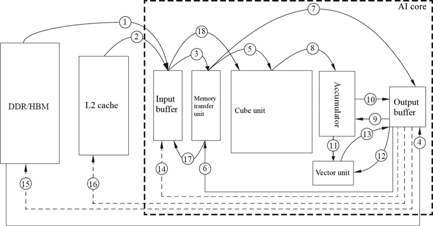
When both the left and right matrix data are ready, the Matrix Queue sends the matrix multiplication instruction to the Cube Unit through the data path ⑤. The XI2C and WI2C matrices are grouped into a 16 × 16 matrix, and the Cube Unit performs multiplication operations. If the input matrix is large, the aforementioned steps may be repeated multiple times and accumulated to obtain the Yo as the intermediate result, which is stored in the Cube Unit. After the matrix multiplication is complete, the accumulator will receive the bias term accumulation instruction if the bias values need to be added. The accumulator then reads the bias values from the OB through data channel ⑨, reads the intermediate result Yo in the Cube Unit through data channel ⑧, and accumulates all values to obtain the final output feature matrix Y, which is transferred to the OB through the data path ⑩ and waits for subsequent instructions to be processed.
After the AI Core finishes the convolution operation through matrix multiplications, the Vector Unit will receive the pooling and activation instructions. The output feature matrix Y then enters the Vector Unit through the data path ⑫ to perform pooling and activation operations. The result Y is stored in the OB through the data channel ⑬. It is very convenient that the Vector Unit can perform some special operations, such as activation functions and can also efficiently implement dimensionality reduction, especially for pooling operations. When conducting the computation of a multilayer neural network, the previous layer output Y is transferred from the OB to the IB through the data channel ⑭, to be used as the input to the computation of the next layer of the neural network.
By considering the unique characteristic of computation and data flow in the convolution operation, the DaVinci architecture design considers many optimizations combining the transferring, computing, and control units more effectively. The overall optimization is achieved without compromising the functionality of each module. The AI Core combines the Cube Unit and data buffer efficiently, shortens the data transmission path from transferring to computing, and greatly reduces the system delay.
In addition, the AI Core integrates a large-capacity input and output buffers on the processor, which allows the AI Core to read and buffer sufficient data at one time, reduce the access to the external storage and significantly improve the data transfer efficiency. At the same time, each on-chip buffer has a much higher speed to access than external storage does, the use of a large amount of on-chip buffers greatly improves the data bandwidth in many computations.
Furthermore, based on the structural diversity of the deep neural network, the AI Core adopts a flexible data path, so that data can be quickly moved back and forth among the on-chip buffer, the off-chip storage system, the MTEs, and the computing units. This flexibility aligns well with the computing requirements of the deep neural network with different structures, which empowers the AI Core to have great adaptability for various types of computations.
3.3.2: Architecture comparison
In this section, we will compare the implementation of convolution on the DaVinci architecture of the Ascend AI processor to that on GPUs and TPUs described earlier. Referring to the convolution example in Fig. 2.2, GPUs use GEMM to convert the convolution calculation into a matrix calculation and obtain the output feature maps through parallel processing in multiple clock cycles using massive threads. With SIMD of the stream processor, GPUs execute multiple threads at the same time, and these threads complete an operation step, such as matrix multiplication, activation, or pooling, in a certain period. After threads in the GPU complete a step, data needs to be written back to the memory because the on-chip memory capacity is small. When the threads execute the next calculation, the data in the memory is read in again. Aimed at the general purpose of computations, GPUs process in similar schemes for convolution, pooling, and activation operations.
Although GPUs achieve flexible task allocation and scheduling control through centralized register management, multithread parallel execution, and CPU-like structure, the overall power consumption is increased. The advantage of centralization is that it facilitates the development of programs. However, in order to meet the general purpose requirement, each computation process needs to comply with the common rules. For example, one rule is that each computation needs to read data from a register and save the result back to the register. In this way, the power consumption of data transfer increases, and GPUs are always considered to be power hungry.
On the other hand, Google’s TPU adopts the systolic array, which directly accelerates the convolution operation. The TPU has a large-capacity buffer on the processor. It can read almost all the data required for convolution operation to the on-chip buffer at once. After that, the data flow control unit transfers the data in the buffer to the computing array for the convolution computation. When all the computing units of the systolic array are fully occupied, the saturation is reached. At each clock cycle, TPU outputs the convolution results of one line. After the convolution operation on the systolic array is finished, the TPU uses a customized vector operation unit to perform activation or pooling.
During the calculation of the convolution neural network, the TPU reads a large amount of data into the buffer at a time by using simplified instructions and uses a fixed data flowing mode to fed the data into the systolic array, which greatly reduces the number of times data must be moved and reduces the overall power consumption of the system. However, this highly customized design limits the scope of the applications supported by the processor. In addition, because the buffer occupies too large a portion on the processor, other valid resources are inevitably compressed, thereby limiting the overall capability of TPU.
The Ascend AI processor accelerates convolution operation through matrix multiplication. First, the input feature map and the weight matrix are reconstructed to perform convolution using matrix multiplication. This is similar to GPU which also uses matrix multiplication to implement convolution calculation. However, due to different hardware architecture and design, the Ascend AI processor differs significantly from the GPU in matrix processing operations. First of all, the Cube Unit in the Ascend AI processor can perform calculations on matrices with size 16 × 16 at a time. Therefore, the throughput rate of the matrix calculation is greatly improved compared with that of the GPU. In addition, due to the careful design of the Vector and Scalar Unit, multiple computations such as convolution, pooling, and activation can be concurrently processed, which further improves the computation parallelism of the deep neural network.
The high computational efficiency in matrix or convolution operations of Ascend AI processor is due primarily to the advanced hardware design used by the DaVinci architecture, which significantly accelerates 16 × 16 matrix multiplications. In addition, DaVinci architecture uses a large number of distributed caches to cooperate with computing units, which effectively reduces data transmission to various computation units. As a result, it improves computing power and reduces the power consumption of data transmission simultaneously. Therefore, Ascend AI processors have huge advantages in the applications of deep convolution neural networks, especially in large-scale convolution calculations. However, because the DaVinci architecture adopts a fixed 16 × 16 Cube Unit when processing a small neural network, the computing power of Ascend AI processors cannot be fully utilized due to the low usage of hardware resources.
In conclusion, every architecture has its own pros and cons. It is meaningless to judge whether a hardware architecture is better or worse without specifying certain applications. Even for the same applications, data size and distribution, type of computation and precision requirements, structure, and layout of the neural network, all these affect whether or not a hardware architecture can fully achieve its advantages. Unfortunately, every case needs to be analyzed separately.
Domain-specific processors are becoming more and more important in the near future for computer industries. Unlike traditional ASICs that need to only consider hardware design, its overall performance strongly depends on efficient software operating on the processor as well. In the following chapters, we will introduce methods of software optimization using examples that will help readers to embrace the concepts of software and hardware collaborative programming and to adapt to the computer industry’s new trend in this post-Moore era.