
Power Supplies
Power supplies of MFPs are characterized primarily by two features: one, they are switching power supplies, and two, they have protection from surges in line voltage. Also, machines with laser printers require a high-voltage supply as well as a lower voltage supply. The latter supplies power to the high-voltage supply. In MFPs with inkjet printers, it supplies 24 V as well as voltages below that level. In addition, it may supply a higher voltage to the printer. In machines with laser printers at least six higher voltages are provided to various components of the laser print engine.
The block diagrams of switching power supplies in two Brother MFPs follow (they are reproduced with permission).
POWER SUPPLY PCB OF BROTHER MFC7000FC AND 7200FC
The power supply (Figure 9.1) uses the switching regulator to generate DC power (+24 V, +5 V, and HVDD) from a commercial AC power supply.
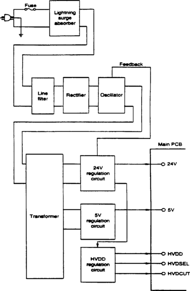
The +24-V source is stabilized and fed to the motors and solenoids for feeding documents and recording paper, as well as to the fluorescent lamp of the CCD unit via the inverter.
The +5-V source is stabilized and fed to the logic, etc.
The HVDD generated from +24 V is fed to the piezoelectric ceramic actuators embedded in the printhead. It is switched between 89 levels within 13 to 30 V depending upon the ambient temperature detected by the head thermistor.
POWER SUPPLY PCB OF BROTHER MFC4350 AND RELATED MODELS
The low-voltage power supply (Figure 9.2) uses the switching regulation system to generate DC power (+5 and +24 V) from a commercial AC power supply to the driver circuits. The +5-V source is fed to the logic control panel, sensors, CIS unit, etc. The 24-V source is fed to the motors, solenoid, fan, and high-voltage power supply PCB.
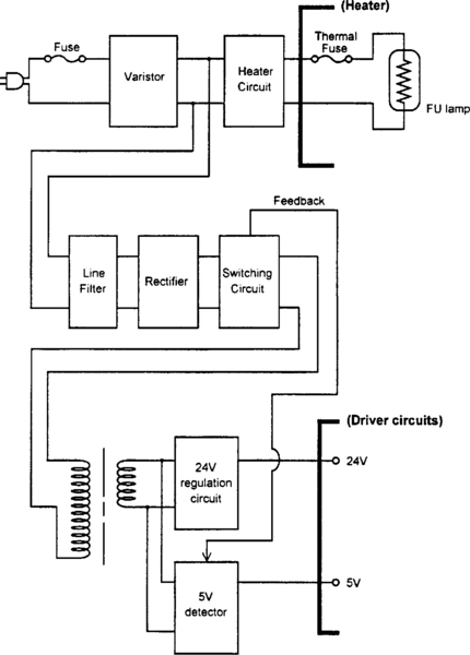
Figure 9.2 Low-voltage power supply block diagram of Brother MFC4250 and related models (Brother International).
The low-voltage power supply also feeds AC power to the heater of the heat-fixing unit.
High-Voltage Power Supply PCB
This power supply (Figure 9.3) generates high-voltage power sources from the 24-V source fed from the low-voltage power supply for charging, developing, and transferring in the laser printing process.

Figure 9.3 High-voltage power supply block diagram of Brother MFC4350 and related models (Brother International).
Switching power supplies are more efficient than conventional nonswitching supplies. Smaller components can be used to provide more compact designs for equivalent output.
In general, the incoming power at 60 cycles is switched at a higher rate into chopped DC, which can be used as a primary signal for a step-down transformer. The duty cycle of the chopped DC is varied to affect the voltage level in the transformer secondary. When the load increases, the output voltage drops. However, this drop is sensed and the duty cycle is adjusted so that the voltage on the secondary increases. The reverse occurs when the load decreases. Thus regulation of the output is realized.
More detail of the operation is given in the following material under the heading “Switching Power Supply Unit Section.” Following that there is a circuit diagram of the switched power supply in the Panasonic KX-F1600, an MFP with an inkjet printer, and the recommended troubleshooting procedures for it. This material is reproduced with the permission of the Panasonic Services Company, a unit of the Matsushita Electric Corporation of America, and is copyrighted by the Kyushu Matsushita Electric Company, Ltd.
SWITCHING POWER SUPPLY UNIT SECTION
See Figure 9.4.
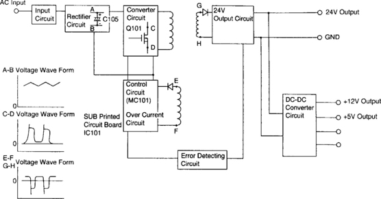
Figure 9.4 Detailed block diagram of switched power supply in KX-F1600 MFP (Kyushu Matsushita Electric Co., Ltd.).
Input Circuit
Input current goes into the input rectifier circuit through a filter circuit. The filter circuit decreases noise terminal voltage and noise electric field strength.
Rectifier Circuit
Input current is rectified by D101 and charge C105 to make DC voltage, then supply power to the converter circuit. Voltage is supplied to control the IC’s kick-on voltage through R102 and R103. Inrush current is limited by thermistor TH101.
Converter Circuit
The converter circuit of this power supply circuit is called a flyback converter. We explain the operation of this circuit with the simple circuit diagram of Figure 9.5.
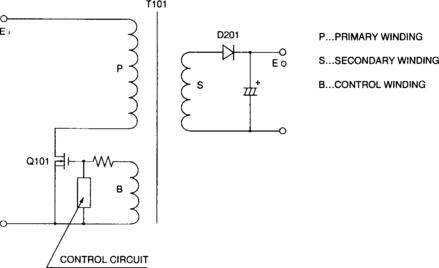
In this circuit, when the transistor Q101 is ON, secondary rectified diode D201 is OFF and the energy is charged in the transformer T101. Q101 continues being ON while the voltage is generated by control winding (B). Q101 is turned OFF by control circuit; then each winding of T101 changes the polarity and rectified diode D201 turns ON.
The charged energy of T101 supplies power through D201 to the output load. The voltage of the control winding is decreased polarity of each winding of T101 in reverse and goes to self-oscillation. When input voltage Ei is high, the ON period of Q101 becomes shorter, and when the load current is high, the ON period of Q101 becomes longer. The value of output voltage is given in Figure 9.6.

In the actual circuit, the fixed output voltage can be obtained by changing the winding ratio of transformer T101. In this converter circuit, the duty ratio of ON period and OFF period of the transistor produces output. In this power supply, the bias winding is also built in to the transformer and the output value is 1. An output voltage of 24 V is stabilized and changes the duty ratio.
Control Circuit and Error-Detecting Circuit
The control circuit amplifies the output with increased voltage detected in the error-detecting circuit, then drives the main transistor. In this power supply the duty ratio is defined by changing the ON period of the main transistor. This is shown as follows.
When the output voltage of the 24-V circuit becomes higher, the current of photo coupler PC101 increases, the pulse width of output control IC becomes narrow, and the ON period of Q101 becomes shorter.
SERVICING THE POWER SUPPLY UNIT
Key Components for Troubleshooting
See Figures 9.7 and 9.8. The following components have been known to break frequently: F101, D101, Q101, IC101, D201, and D210. This has been experienced in experimental tests such as power supply and lighting surge voltage tests, voltage withstand tests, and intentional short circuit tests.
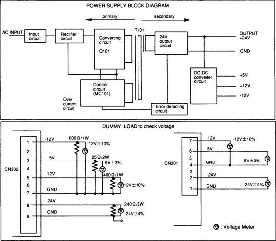
Figure 9.7 KX-F 1600 power supply block diagram and dummy load (Kyushu Matsushita Electric Co., Inc.).

Figure 9.8 Schematic diagram of KX-F1600 switched power supply circuit (Kyushu Matsushita Electric Co., Inc.).
Caution: If a melted fuse is found in the unit, power should not be turned on without first repairing the unit. If only the fuse is replaced, it will melt again. The cause exists elsewhere.
Because of circuit composition, if 24 V is not output, then 5 V, 12 V, and −12 V will not be output. Also, if 5 V is not output, both 12 V and −12 V will not be output.
In most cases, the symptom is that nothing is output. There is a high possibility that the trouble is in the primary side more than the secondary side.
Troubleshooting Flow Chart
Our recommendation for troubleshooting is as follows (Figure 9.9). This procedure comes from experience of troubleshooting in the lab.
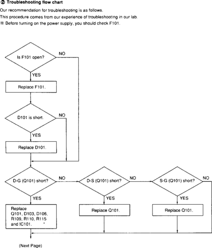
Note: Before turning on the power supply, you should check F101.
Repair Details for Broken Parts
D101: Check short-circuit of terminal 4. If D101 is short-circuited, F101 will be melted (open). So in this case, replace those parts.
Q101: The worst case of Q101 is a short-circuit between the drain and gate because damage expands to IC101 on the sub PC1. This is due to very high voltage through the gate circuit that is composed of D106, D103, R109, R115, and R110. Change all of the parts listed as follows: F101, Q101, D103, D106, R109, R115, R110, IC101.
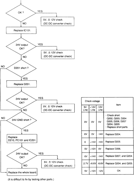
IC101: Occasionally, there occurs the sole case of a broken IC101. You should exchange all of the sub-board to make the repair operation easier.
D201: If D201 is broken, the oscillation circuit of the power supply cannot operate. Check it with an electric tester.
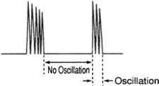
D210: Occasionally, this part short-circuits. In this case, you can listen for the clicking sound of intermittent oscillation (which happens when the power supply balance is broken and loads as a perfect open or short-circuit of output; see the graph in Figure 9.10). Check the resistance between 24 V and GND.
SURGE PROTECTION
When G3 fax machines were first introduced, a principal cause of equipment failure was surges in power-line and/or telephone-line voltages. This was due to the delicate structure of the CMOS integrated circuits, which made them susceptible to damage from voltage and current surges. This vulnerability made it necessary to protect them by using transient-suppression devices in the power input and telephone line interface circuitry. The latter is covered in Chapter 8 (The Fax Function).
Lightning is the most common cause of transients in electronic equipment. However, there are other sources of power disturbances, such as that caused by a refrigerator compressor cycling on and off and affecting electronic equipment on the same line. Static discharge, which results from a sudden and violent redistribution of electrons between two objects, is another cause of failure. It lasts for an extremely short time, but its amplitude can be in the kilovolt range. Such discharges contain little energy, but their fast rise time and high power can devastate sensitive semiconductors. Junction shorting, oxide puncture, or melting of device metalization may occur.
Surge Suppression Devices
In the power supply circuit (Figure 9.8) above CN31, the AC power inlet, surge protector devices can be seen at Z101, Z102, and Z103. In this case, they are shown as varistors in the parts list. Thyristors are also used in other designs as shown in Figure 9.2.
Varistors usually bear the symbol “Z” and thyristors are shown as “Z”.
These varistors are metal-oxide and are designated by the abbreviation MOV. The resistance of these nonlinear devices varies with applied voltage. They are usually in a disk shape and consist of ceramic-like material. To ensure uniform current distribution, the disk’s surface is coated with a highly conductive metal and is encapsulated with a plastic-epoxy material. The interface between the zinc-oxide and the metal-oxide matrix material is roughly equivalent to two back-to-back pn junctions. Therefore, the MOV can be viewed as several pn junctions in a series-and-parallel configuration. This gives the MOV a characteristic curve similar to back-to-back zener diodes. It turns on in a few nanoseconds and has high clamping voltages ranging up to as much as 1.5 kV
With each transient event MOVs gradually deteriorate. Their granular interfaces overheat. They begin to short and there is a gradual decrease in breakdown voltage. However, under average circumstances, their life expectancy may be compatible with other components of the equipment.
Transient-voltage-suppressor (TVS) thyristors are solid-state devices constructed with four alternating layers of p- and n-type material. Their structure is similar to an SCR whose gate is controlled by an avalanche zener diode. They are crowbar devices that switch to a low on-state voltage when triggered. The TVS thyristor can conduct high surge currents because its on-state voltage is low. The current through the device must fall below the holding current for the device to return to a non-conducting state. TVS thyristors do not wear out. They respond in nanoseconds. Their unique characteristics make them well suited as surge protection devices.