
CONTENTS
67.2 Micromagnetic Solver and Benchmarks with Experimental Data
67.3.3 Partially Perpendicular
67.4 Switching Speeds of Different Classes of Ferromagnetic Materials
67.4.1 Low versus High HK In-Plane Materials
67.4.2 In-Plane versus Perpendicular Materials
67.4.3 In-Plane versus Partially Perpendicular Materials
Owing to the physical and electrical scaling challenges, the MOSFET-based memory industry (Flash, DRAM, SRAM, etc.) is predicted to hit the end of the road in the near future. Not only do MOSFET-based memories have scalability issues, but also they face increased power leakage and endurance problems [1,2 and 3]. A lot of effort is accordingly being invested into alternate forms of information storage to sustain Moore’s law for memory over the next decades.
A possible road forward is to store information by using the spin degree of freedom of electrons, instead of charge-based storage that most MOSFET-based memory technologies follow. Spin-transfer torque random access memory (STT-RAM) is one of the frontrunners in spin-based memory technology today [4,5]. STT-RAM devices are based on magnetic tunnel junctions (MTJs) that can store a bit of information (Figure 67.1) [6]. A typical MTJ consists of two ellipsoidal ferromagnetic films separated by an insulating spacer film. The magnetization of one ferromagnetic layer (the fixed layer) is pinned by exchange coupling with an antiferromagnetic layer, while the magnetization of the second (free) layer can change freely. Data in an MTJ can be retained in the relative spin orientations of the fixed and free ferromagnetic layers (bit ‘0’ or low resistance for parallel (P) and bit ‘1’ or high resistance for antiparallel (AP)). The stored data can thereafter be sensed by measuring the tunneling magnetoresistance (TMR) [7]. Data are written by switching the magnetization of the free layer by direct transfer of the spin angular momentum from the torque due to a current injected across the insulator, spin polarized by the fixed layer [8,9]. Figure 67.2 shows the simulation results from a comprehensive STT-RAM model, combining non-equilibrium Green’s function with macrospin dynamics [10,11] with parameters extracted from a published, in-plane rectangular 70 × 250 nm CoFeB/MgO/CoFeB (2 nm) [12] MTJ. AP to P switching was observed to take place in 10 ns at 0.26 V and P to AP switching at 0.38 V, consistent with the experimental data. The tunneling magnetoresistance is 154% near 0 V.
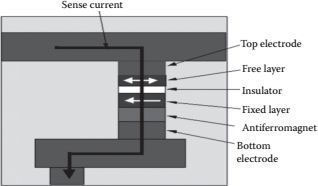
FIGURE 67.1 Magnetic tunnel junction—two ferromagnetic layers separated by an insulating spacer layer. The magnetization of one ferromagnetic layer (the fixed layer) in the MTJ is pinned by exchange coupling with an antiferromagnetic layer, while the magnetization of the second (free) layer can change by a spin-transfer torque.
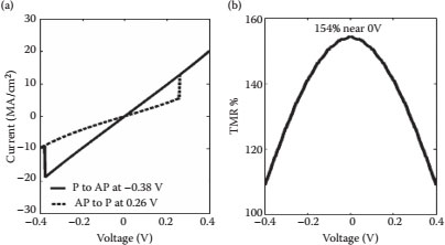
FIGURE 67.2 (a) STT-RAM simulation result with parameters extracted from the published CoFeB/MgO/CoFeB MTJ [1], [2] experiment. In our simulations, the AP to P switching was observed to take place at 0.26 V and P to AP switching at −0.38 V given within a 10 ns pulse, matching the experimental switching voltages quite well. (b) Tunneling magnetoresistance is 154% near 0 V, in agreement with the experiments.
With the help of the comprehensive model, we can study how AP to P and P to AP switching happens in an STT-RAM cell. AP to P switching occurs in the free layer when a positive voltage is applied to the free layer relative to the fixed layer (Figure 67.3). A majority of the electrons with respect to the fixed layer tunnel through the barrier and build up at the free layer, as shown in Figure 67.3b, adding angular momentum and exerting a torque. After enough majority spin is accumulated to exert a critical torque, the free layer starts switching from the antiparallel to the parallel configuration at 2.6 ns. By 5 ns, the magnetization of the free layer has completed its switching from the antiparallel to the parallel mode. Conversely, for P to AP switching (Figure 67.4), a negative voltage is applied on the free layer. At 0 ns, the free layer is parallel but slightly noncollinear to the fixed layer (at room temperature, thermal torques ensure slight deviation from strict collinearity). At 6 ns, a majority of the electrons with respect to the fixed layer tunnel through the barrier, while the antiparallel minority electrons build up at the free layer, reducing its angular momentum. The accumulated downspin electrons create a torque on the free layer, causing it to switch from up to down. By 8 ns, the final magnetization of the free layer is antiparallel to the fixed layer. In short, the switching mechanism is the progressive addition or removal of majority spins relative to the fixed layer, creating a torque at the site of the free layer.
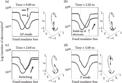
FIGURE 67.3 AP to P switching using CoFeB/MgO/CoFeB MTJ parameters at 0.4 V applied to the free layer. The starting angle is taken to be root-mean-square of the initial thermal distribution, θrms. (a) Time = 0 ns: The free layer is almost antiparallel to the fixed layer, (b) Time = 2.2 ns: A majority of the electrons with respect to the fixed layer tunnel through the barrier and build up at the free layer. The accumulated majority of electrons exerts a torque on the free layer, which causes its magnetization to start switching. (c) Time = 2.6 ns: The free layer continues switching from the antiparallel to the parallel configuration. (d) Time = 5 ns: The final magnetization of the free layer is parallel to the fixed layer.
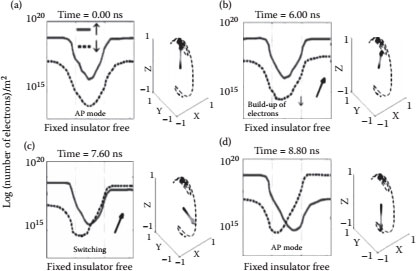
FIGURE 67.4 P to AP switching at −0.4 V applied to the free layer. (a) Time = 0 ns: The free-layer is almost parallel to the fixed layer. (b) Time = 6 ns: The magnetization of the free layer is non-collinear with respect to the fixed layer magnetization. A majority of the electrons with respect to the fixed layer tunnel through the barrier, while the residual antiparallel minority electrons build up at the free layer. The accumulated down spin electrons create a torque on the free layer, causing it to start switching from the up to down. (c) Time = 7.6 ns: The free layer continues switching from the parallel to the antiparallel configuration. (d) Time = 8 ns: The final magnetization of the free layer is antiparallel to the fixed layer.
The critical current densities for spin torque switching in STT-RAMs is nonetheless too high for commercial applications, prompting intense investigation into material properties of the free layer [13]. The energy dissipation during the spin-transfer torque switching is given by I2Rτ, where I is the current used to induce spin-transfer torque switching, R is the resistance of the MTJ, and τ is the total delay time it takes for the magnetization of the free layer to switch. In this work, for a given spin-polarized current density, J, of 2 MA/cm2, we study the switching speed τ of different classes of magnetic materials, in-plane, perpendicular, and partially perpendicular (Figure 67.5) at 0 K temperature. We consider the free layer at the 45 nm feature STT-RAM technology, and employ a single-domain macrospin solver that solves the Landau–Lifshitz–Gilbert (LLG) equation [14]. For enough stability against thermally driven switching, to retain data for at least 10 years, Δ needs to be greater than 75 at room temperature [15]. The voltage needed to generate a current of such magnitude, and thus the resistance R, will be dependent on the material and insulator properties, such as the effective masses, insulator thickness, band-offset, and contact polarizations. Extracting the MTJ resistance corresponding to a given I will require the solution of the quantum transport problem using the non-equilibrium Green’s function formalism (NEGF) [10] or, in a simpler incarnation, the Simmons model for tunneling across a barrier, modified to include its crucial magnetizationdependent prefactors [11,16]. While such a coupled transport-macromagnetic study is ultimately needed for overall energy efficiency studies, the aim of this chapter is to identify materials for fast switching in STT-RAM within 10 ns, with acceptable thermal stability (Δ > 75).
A proper model for spin torque-induced switching should include thermal effects, which provide the initial torque to nudge the magnetization away from stagnation points along the energy landscape (i.e., away from strict parallel or antiparallel configurations), while at the same time hindering the motion of the magnetization on its journey past stagnation. In Ref. [11], we include an average over the thermal distribution of the initial angle evaluated using a Fokker–Planck equation. In this chapter, we simplify this treatment by directly replacing the initial angle with the root mean squared value θrms at 300 K, set by the equipartition theorem. While thermal agitation during the course of the reversal adds some uncertainty to the final delay time, the difference is likely to be small [17]. Therefore, we will disregard thermal effect during the course of reversal in this work.
In Section 67.2, the macrospin simulator that solves the LLG equation is introduced, and benchmarks with experimental results are shown. Section 67.3 outlines the critical switching currents and thermal stabilities for the in-plane, perpendicular, and partially perpendicular ferromagnetic free layers. Section 67.4 describes the variation in switching speeds across the material classes for a given switching current density, providing a path for the STT-RAM industry for fast, reliable switching.
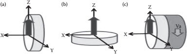
FIGURE 67.5 Definition of the magnetization of the free ferromagnetic layer in a spherical coordinate system. Magnetization for (a) In-plane material: the easy axis is along the major axis, Z, of the ellipsoidal plane,. (b) Perpendicular material: the easy axis is perpendicular to the disk. (c) Partially-perpendicular: an in-plane disk is capped with a vanadium layer that reduces the demagnetization anisotropy of the system by antiferromagnetic exchange coupling. In all three cases, magnetization prefers to lie near θ = 0 (parallel case) or θ = π (antiparallel case). (K. Munira, W. A. Soffa, and A. W. Ghosh, Comparative material issues for fast reliable switching in STT-RAMs, 2011 11th IEEE Conference on Nanotechnology (IEEE-NANO), pp. 1403–1408, © (2011) IEEE. With permission.)
67.2 MICROMAGNETIC SOLVER AND BENCHMARKS WITH EXPERIMENTAL DATA
The magnetization dynamics of the free layer is modeled by solving the modified LLG equation including spin torque [14]
(67.1) |
(67.2) |
where and are the unit magnetization vectors of the free layer and the spin-polarized current density, respectively, α is the Gilbert damping coefficient, MS is the saturation magnetization, γ is the gyromagnetic ratio, and is the effective magnetic field that includes the effects of magnetocrystalline and shape anisotropy. The spin-transfer torque is introduced by the current I of polarization η. The initial angle for all materials is set at the root mean square θ of the free layer nanomagnets under thermal perturbation, calculated by the equipartition theorem (Figure 67.6), sin2 (θrms) = 1/2Δ [18]. Note that we are including only the current-induced spin torque in our treatment. The “field-like” direct exchange torque between the layers can also play a role in switching, although it is typically significantly weaker than the purely current-driven term.
The current values entering the above equation are benchmarked separately by fitting NEGF simulation results with multiple STT-RAM experiments. In experiments on in-plane rectangular 70 × 250 nm CoFeB/MgO/CoFeB (2 nm) [12], AP to P switching was observed to take place at 0.26 V and P to AP switching at −0.38 V with a spin-polarized current density ηJ = 28.5 MA/cm2, given a 10 ns pulse. Using HK of 39.78 KA/m, MS of 1050 KA/m, and Gilbert damping of 0.02 in our LLG model, our NEGF simulation reproduces these results. Indeed, with ηI = 28.5 MA/cm2, we find that a current pulse of at least 10 ns is needed for switching. For AP to P switching, voltages greater than −0.38 V are unable to switch the free ferromagnet within 10 ns as seen in Figure 67.7. Similarly, for P to AP switching, negative voltages weaker than 0.26 V are unable to switch within 10 ns (Figure 67.8). Our NEGF currents that agree with the experimental values are thereafter incorporated into the simplified LLG solver above, through the I term that enters the torque.
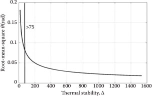
FIGURE 67.6 Thermal stability, Δ, vs. root-mean-square, θrms(rad) of the free layer nanomagnet. Δ needs to be greater than 75 for commercial applications. Root-mean-square θrms(rad) identifies the initial angle that we use in our simulations. (K. Munira, W. A. Soffa, and A. W. Ghosh, Comparative material issues for fast reliable switching in STT-RAMs, 2011 11th IEEE Conference on Nanotechnology (IEEE-NANO), pp. 1403–1408, © (2011) IEEE. With permission.)
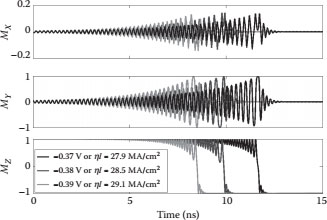
FIGURE 67.7 Parallel to antiparallel switching takes place in an in-plane CoFeB/MgO/CoFeB magnetic tunnel junction [1] at −0.38 V, given a 10 ns pulse of spin current, with a spin current density, ηJ = −28.5 MA/cm2. A current pulse of at least 10 ns is needed for switching at −0.38 V. Voltages greater than −0.38 V will not be able to switch the free ferromagnet within 10ns as shown in the figure. HK of 39.78 KA/m, MS of 1050 KA/m, and Gilbert damping of 0.02 were used. The magnetization of the free ferromagnet switches from θ ≈ 0 to θ ≈ π. MZ = cos θ: The simulation results agree quantitatively with the experiments [1]. (K. Munira, W. A. Soffa, and A. W. Ghosh, Comparative material issues for fast reliable switching in STT-RAMs, 2011 11th IEEE Conference on Nanotechnology (IEEE-NANO), pp. 1403–1408, © (2011) IEEE. With permission.)
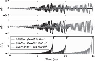
FIGURE 67.8 Antiparallel to parallel switching takes place in an in-plane CoFeB/MgO/CoFeB magnetic tunnel junction [1] at 0.26 V, given a 10ns pulse of spin current, with a spin current density ηJ = 28.5MA/cm2. A current pulse of at least 10 ns is needed for switching at 0.26 V. Voltages less than 0.26 V will not be able to switch the free ferromagnet within 10 ns as shown in the figure. The magnetization of the free ferromagnet switches from θ ≈ π to θ ≈ 0. The simulation results agree quantitatively with the experiments [1]. (K. Munira, W. A. Soffa, and A. W. Ghosh, Comparative material issues for fast reliable switching in STT-RAMs, 2011 11th IEEE Conference on Nanotechnology (IEEE-NANO), pp. 1403–1408, © (2011) IEEE. With permission.)
67.3 CRITICAL SWITCHING CURRENTS AND THERMAL STABILITIES FOR VARIOUS CLASSES OF FREE LAYER MAGNETIC MATERIALS
Figure 67.5 defines our choice of axes and angular conventions that we will adopt for the different material classes. For in-plane materials, the easy axis is aligned along the major axis of the ellipsoidal plane (Figure 67.5a). For a 45 nm feature technology, the free layer ellipsoidal disk has a minor axis of 45 nm, a major axis of 90 nm, and a thickness of 2 nm [15]. The potential energy density for an in-plane system is defined by its magnetocrystalline anisotropy and demagnetization field, . The critical current for switching is
(67.3) |
HK is the magnetocrystalline anisotropy field, MS is the saturation magnetization, and Ω is the total volume of the free layer. The thermal stability is
(67.4) |
The switching time required at zero temperature [17] for the initial angle, θrms, and applied current, I, is
(67.5) |
The easy axis is perpendicular to the plane (Figure 67.5b). For a 45 nm feature technology, the free layer circular disk has a diameter of 90 nm and a thickness of 2 nm [15]. The potential energy density for the system is defined by its magnetocrystalline anisotropy and demagnetization field,. The critical current for switching [19] is
(67.6) |
The decreased barrier reduces the critical current but also has an adverse effect on thermal stability
(67.7) |
Materials with higher saturation magnetization will have less thermal stability, making the range of reliable materials narrower. Most perpendicular materials require epitaxial growth at elevated in situ temperatures, making them harder to integrate with CMOS processes than in-plane MTJ materials. They also typically have higher damping constants α than in-plane MTJ free layer materials [20, 21, 22 and 23]. The switching time required at zero temperature for initial angle, θrms, and applied current, I, is
(67.8) |
67.3.3 PARTIALLY PERPENDICULAR
An in-plane material is capped antiferromagnetically with a vanadium cap (Figure 67.5c) that reduces the demagnetization field of the disk [24,25]. The term “partially perpendicular” is used because the overall switching barrier is being reduced as in perpendicular materials (by the demagnetization field in the later case), but the magnetization still lies in the plane of the elliptical disk. The potential energy density for the system is defined by its magnetocrystalline anisotropy, demagnetization field, and exchange coupling with the capping layer, , where Ki (J/m2) is the interfacial energy between the free layer and capping and tfreelayer (nm) is the thickness of the free layer. In Ref. [24], for a 2 nm CoFeB free layer capped with vanadium, we see an 85% decrease in the demagnetization field. The critical current for switching is
(67.9) |
where H⊥ is the reduced demagnetization field. Thermal stability is the same as the in-plane materials. The switching time required at zero temperature for initial angle, θrms, and applied current, I, is
(67.10) |
67.4 SWITCHING SPEEDS OF DIFFERENT CLASSES OF FERROMAGNETIC MATERIALS
The previous section lists the critical currents that correspond to a destabilization of the initial magnetization from their respective easy axes toward the harder axes. To actually accomplish the switching in a given time, we will need to inject a substantially larger current. The switching time depends on the interactive dynamics between the various effective fields along the trajectory of the switching magnetization. Figures 67.9 through 67.11 show the switching delays of the in-plane, perpendicular, and partially perpendicular materials with varying MS, HK, and α, given a current density of 2 MA/cm2. The phase plots designate the switching times, while those enclosed by the white boundaries identify the range of suitable materials that successfully switch within 10 ns (using Equations 67.5, 67.8, and 67.10) with a Δ > 75 (using Equations 67.4 and 67.7). Table 67.1 lists the set of industrially relevant STT-RAM free layer materials that we study. Numerically calculated HK and MS combinations that switch within 10 ns and solutions of Equations 67.5, 67.8, and 67.10 for the in-plane, perpendicular, and partially perpendicular materials are compared in Figure 67.12. The numerical and analytical results are in agreement.
We can rationalize the shapes of the phases and white polygons designating efficient switching by outlining the various constraints they need to satisfy. In particular, we find that in-plane materials with low MS and low HK tend to switch faster, as their switching energy barrier to the spin current is proportional to . Perpendicular materials with low MS and low HK also switch faster, their barriers being proportional to . Even though a higher MS also cuts down the energy barrier through the negative term, materials with high HK do not help switching, as the dominant energy term is proportional to HKMS.
67.4.1 LOW VERSUS HIGH HK in-PLANE MATERIALS
For a given MS, we find that materials with high HK switch almost as fast as low-HK materials. This seems counterintuitive, as a higher HK yields a higher switching barrier Δ and a correspondingly low initial angle θrms. The explanation lies in the effective magnetic fields during the first half (initial configuration to equator) versus the second half (equator to flipped configuration) of the switching process. Figure 67.13 shows simulations with the saturation magnetization set at 200 KA/m and HK set to 159.15 KA/m (top) and 1591.5 KA/m (bottom). To isolate the field dynamics, the same spin current of 2 MA/cm2 is applied to the two systems, and the starting θ angle is set to 0.129 rad in each case. At 159.15 KA/m, the magnetization takes 0.5 ns to come to the equator and then another 0.4 ns to reach the south pole. At 1591.5 KA/m, the magnetization takes 1.03 ns to come to the equator, but only 0.22 ns to come to the south pole. What is noteworthy is the unequal times taken for the two switching steps. The asymmetry arises because while the high anisotropy field hinders the magnetization from moving from the north pole to the equator, it helps while moving from the equator to the south pole. Therefore, the large amount of time taken to travel to the equator at high HK is compensated by the fast switching from the equator to the north pole.
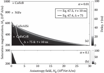
FIGURE 67.9 Numerically calculated switching delay (ns) for in-plane materials with varying saturation magnetization (MS), anisotropy field (HK), and Gilbert damping (a) α = 0.01 and (b) α = 0.1. A current density of 2 MA/cm2 is applied. Materials that switch faster, <10 ns with thermal stability greater than 75, are preferred and are indicated by the area enclosed by the white boundaries. The white solid line indicates the boundary where Δ is 75 (using Equation 67.4, which defines a rectangular hyperbola), while the dashed line indicates the boundary where the switching time is 10ns (using Equation 67.5, another rectangular hyperbola). Compared to materials with α = 0.01, materials with α = 0.1 rarely switch. At α = 0.01 and low magnetization, materials with low and high HK switch at the same speed, even though the energy barrier that the spin current needs to overcome is proportional to . The explanation for this is outlined in Figure 67.12. (K. Munira, W. A. Soffa, and A. W. Ghosh, Comparative material issues for fast reliable switching in STT-RAMs, 2011 11th IEEE Conference on Nanotechnology (IEEE-NANO), pp. 1403–1408, © (2011) IEEE. With permission.)
In summary, in-plane materials with high HK and low MS would be good candidates for the free layer. The high HK promotes high thermal stability, and does not compromise on switching speed because it actually helps with the switching process from the hard axis to the south pole.
67.4.2 IN-PLANE VERSUS PERPENDICULAR MATERIALS
Figure 67.14 shows the difference between in-plane and perpendicular magnetization switching at 2 MA/cm2, HK = 159.15 KA/m, MS = 500 KA/m, and α = 0.01. Recall that for in-plane magnetization switching, both the anisotropy and demagnetization fields hinder the switching from the north pole to the equator, and both fields help the switching from the equator to the south pole. For perpendicular magnetization switching on the other hand, the anisotropy field opposes while the demagnetization field helps the switching from the north pole to the equator. However, after passing the equator, the anisotropy helps in moving to the south pole, while the demagnetization field opposes it. Thus, the times taken for the magnetization to travel from the north pole to the equator and then from the equator to the south pole are comparable.
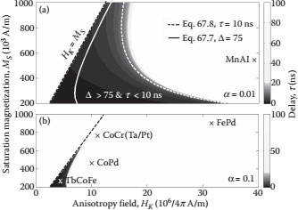
FIGURE 67.10 Numerically calculated switching delay (ns) for perpendicular materials with varying saturation magnetization (MS), anisotropy field (HK), and Gilbert damping: (a) α = 0.01 and (b) α = 0.1. A current density of 2 MA/cm2 is applied. Overall, perpendicular materials switch faster than in-plane materials, as the energy barrier that the spin current needs to overcome is proportional to . However, the decreased barrier has an adverse effect on thermal stability, . For increased MS, thermal stability is reduced, making the range of reliable materials narrower. Most perpendicular materials have α = 0.1. Materials that switch within 10 ns and Δ greater than 75 are preferred and are indicated by the enclosed area by the white boundaries. The white solid line indicates the boundary where Δ is 75 (using Equation 67.7, which defines a rectangular hyperbola added to a linear term), while the dashed line indicates the boundary where the switching time is 10 ns (using Equation 67.8). Even though higher MS cuts down the energy barrier, materials with high HK do not switch as the dominant energy barrier term is proportional to HKMS. The shape of the colored region is bounded to the left by a linear separatrix that corresponds to maintaining a perpendicular magnetization, . (K. Munira, W. A. Soffa, and A. W. Ghosh, Comparative material issues for fast reliable switching in STT-RAMs, 2011 11th IEEE Conference on Nanotechnology (IEEE-NANO), pp. 1403–1408, © (2011) IEEE. With permission.)
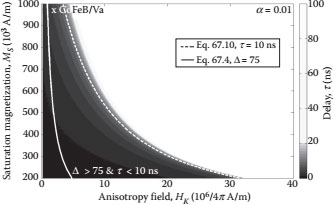
FIGURE 67.11 Numerically calculated switching delay (ns) for partially-perpendicular materials with varying saturation magnetization (MS), anisotropy field (HK), and α = 0.01. The demagnetization is reduced by 85% by capping. A current density of 2MA/cm2 is applied. A wider range of materials (indicated by the enclosed area by the white boundaries using Equations 67.4 and 67.10) switch within 10 ns with a thermal stability greater than 75, as compared to in-plane materials with α = 0.01, generating thereby a more suitable class of free layer materials. (K. Munira, W. A. Soffa, and A. W. Ghosh, Comparative material issues for fast reliable switching in STT-RAMs, 2011 11th IEEE Conference on Nanotechnology (IEEE-NANO), pp. 1403–1408, © (2011) IEEE. With permission.)
TABLE 67.1
A List of Ferromagnetic Materials That Are Being Investigated for the Free Layer in STT-TAM
Material |
Anisotropy Field, Hk (103/4 π KA/m) |
Saturation Magnetization, MS (KA/m) |
α |
|| or ⊥ |
TbCoFe [21] |
1.2 |
139 |
0.1 |
⊥ |
0.5 |
1050 |
0.01 |
|| |
|
FePd [22] |
33 |
1100 |
0.1 |
⊥ |
FePt [22] |
116 |
1140 |
0.1 |
⊥ |
Co2FeAl0.5Si0.5 [28] |
0.3 |
560 |
0.01 |
|| |
MnAl [22] |
61 |
560 |
0.01 |
⊥ |
10 |
450 |
0.1 |
⊥ |
|
0.25 |
800 |
0.01 |
|| |
|
CoPt [31] |
91 |
900 |
0.1 |
⊥ |
CoFeGe [32] |
5 |
350 |
0.1 |
⊥ |
CoFeCrB [32] |
0.1 |
350 |
0.01 |
|| |
CoCrPt [33] |
14.2 |
800 |
0.1 |
⊥ |
CoCrTa [33] |
12.2 |
800 |
0.1 |
⊥ |
Note: || stands for in-plane materials while ⊥ for perpendicular materials.
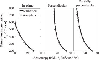
FIGURE 67.12 Numerically calculated HK and MS combinations that switch within 10ns, overlaid with solutions of Equations 67.5, 67.8, and 67.10 for in-plane, perpendicular and partially-perpendicular materials. The numerical and analytical results are in excellent agreement.
For comparable Gilbert damping α, a wider range of perpendicular materials switch than in-plane materials, the energy barrier being proportional to (Figure 67.10a). The steep curve to the right of the colored region at 100 ns coalesces ultimately with the linear boundary to the left that corresponds to , in other words, maintaining a perpendicular magnetization. The white polygon includes the additional inequality Δ > 75, which gives a rectangular hyperbola on the MSHK plot. Unfortunately, most perpendicular materials known today have high Gilbert damping, making them undesirable for STT-RAM use (Figure 67.10b).
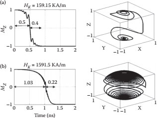
FIGURE 67.13 For in-plane materials with α = 0.01 and low magnetization, materials with low and high HK switch at almost the same speed, even though the energy barrier that the spin current needs to overcome is proportional to . The above figure shows two cases where the saturation magnetization is fixed at (200 KA/m), and the HK of (a) 159.15 KA/m and (b) 1591.5 KA/m are used for the LLG simulations. At 159.15 KA/m, the magnetization takes 0.5 ns to come to the equator and then another 0.4 ns to come to the south pole. At a larger HK of 1591.5 KA/m Oe, the magnetization takes 1.03 ns to come to the equator but only 0.22 ns to come to the south pole. The asymmetry arises because the high magnetocrystalline anisotropy field hinders the magnetization while moving from the north pole to the equator, but assists it while moving from the equator to the south pole. Thus, the longer time taken to reach the equator at higher HK is compensated for by the faster switching from the equator to the south pole. (K. Munira, W. A. Soffa, and A. W. Ghosh, Comparative material issues for fast reliable switching in STT-RAMs, 2011 11th IEEE Conference on Nanotechnology (IEEE-NANO), pp. 1403–1408, © (2011) IEEE. With permission.)
Perpendicular materials with a low damping constant will be good candidates for STT-RAM free layers. Their switching speeds will be comparable to in-plane materials, but there will be a greater probability of switching.
67.4.3 IN-PLANE VERSUS PARTIALLY PERPENDICULAR MATERIALS
A wider range of partially perpendicular materials switch within 10 ns when compared to in-plane materials, making partially perpendicular materials ultimately a more energy-efficient class of materials. Their dampings at α = 0.01 are small, yet their barriers are reduced by an overall negative term, allowing a wide range of fast switching events. Figure 67.15 shows the difference between in-plane and partially perpendicular magnetization switching at 2 MA/cm2, HK = 1591.5 KA/m, MS = 500 KA/m, and α = 0.01. The decrease in the demagnetization field causes the magnetization to switch three times faster. Capping in-plane materials with a Va layer should be further investigated as their fast switching speed shows great promises for low-energy switching.
A wide variety of materials, cataloged into three magnetic classes, are explored for their switching speeds at a given thermal stability and switching current density. To be considered a suitable candidate for the free layer in STT-RAM, the material needs to conform to three requirements: (1) high
thermal stability to prevent soft error, (2) ability to switch with low applied spin current, and (3) high switching speed, as the energy consumed during the write process is proportional to the total time it takes to switch. For faster and more reliable energy-efficient switching in the thermally stable free layer of an STT-RAM, the following material paths should be taken: (a) in-plane materials with high HK and low MS (high HK increases the speed of switching, especially during the second half, and has greater thermal stability); (b) perpendicular materials with low damping—reaching comparable switching speeds with in-plane but with greater probability to switch; and (c) antiferromagnetically capped partially perpendicular materials—capping with a Va layer decreases the demagnetization field, which enables the switching to occur faster without compromising the thermal stability. It is worth emphasizing at this stage that the study presented here is entirely based on the magnetic properties of the contacts, as captured by LLG. A separate material phase space will correspond to the electronic properties and ultimately the voltage required to generate the drive current, namely, the contact and barrier effective masses, tunnel barrier height and width, and the polarization in the contacts [11]. These can be extracted and studied using the NEGF equation, and alternately using a modified Simmons equation. While the LLG study yields the critical current density and switching speeds, the Simmons equation would, in addition, provide the switching voltages, that is, the tunnel barrier resistances required to accomplish these switching events, thereby providing the total energy dissipated during the switching event.
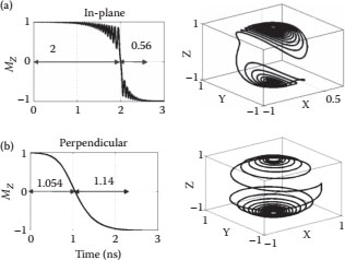
FIGURE 67.14 Difference between (a) in-plane and (b) perpendicular magnetization switching at 2 MA/cm2, HK = 159.15 KA/m, MS = 500 KA/m, and α = 0.01. For in-plane magnetizations, both the magnetocrystalline anisotropy and demagnetization fields hinder the magnetization during the north pole to the equator transition. After passing the equator, both fields help in moving to the south pole. For perpendicular magnetizations, the anisotropy field opposes, while the demagnetization field helps the magnetization move from the north pole to the equator. After passing the equator, the anisotropy helps while the demagnetization field opposes the subsequent equator to south pole switching. Thus, the times taken for the north pole to equator and equator to south pole transitions are comparable. (K. Munira, W. A. Soffa, and A. W. Ghosh, Comparative material issues for fast reliable switching in STT-RAMs, 2011 11th IEEE Conference on Nanotechnology (IEEE-NANO), pp. 1403–1408, © (2011) IEEE. With permission.)
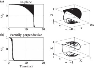
FIGURE 67.15 Difference between (a) in-plane and (b) partially-perpendicular magnetization switching at 2MA/cm2, HK = 1591.5 KA/m, MS = 500 KA/m, and α = 0.01. The decrease in the demagnetization field causes the magnetization to switch 3 times faster for the latter case. (K. Munira, W. A. Soffa, and A. W. Ghosh, Comparative material issues for fast reliable switching in STT-RAMs, 2011 11th IEEE Conference on Nanotechnology (IEEE-NANO), pp. 1403–1408, © (2011) IEEE. With permission.)
K. Munira thanks E. Chen of Grandis Inc. for discussions on a variety of switching materials, A. Natarajarathinam and W. H. Butler of the University of Alabama for discussions on perpendicular and partially perpendicular materials, and A. Nigam and Mircea Stan of the University of Virginia for discussions regarding the macromagnetic solver.
1. G. Atwood, Future directions and challenges for ETox flash memory scaling, IEEE Trans. Device Mater. Reliab., 4(3), 301–305, 2004.
2. R. Baumann, Soft errors in advanced computer systems, IEEE Des. Test Comput., 22(3), 258–266, 2005.
3. D. Frank, R. Dennard, E. Nowak, P. Solomon, Y. Taur, and H.-S. P. Wong, Device scaling limits of Si MOSFETs and their application dependencies, Proc. IEEE, 89(3), 259–288, 2001.
4. V. Zhirnov, J. Hutchby, G. I. Bourianoff, and J. Brewer, Emerging research memory and logic technologies, IEEE Circuits Devices Mag., 21(3), 47–51, 2005.
5. S. A. Wolf, D. D. Awschalom, R. A. Buhrman, J. M. Daughton, S. von Molnr, M. L. Roukes, A. Y. Chtchelkanova, and D. M. Treger, Spintronics: A spin-based electronics vision for the future, Science, 294(5546), 1488–1495, 2001.
6. E. Hirota, H. Sakakima, and K. Inomata, Magnetic random access memory (MRAM). In: Giant Magneto-Resistance Devices, G. Ertl, R. Gomer, H. Luth, and D. Mills (Eds.), Springer, Berlin, Germany, pp. 135–136, 2002.
7. M. Julliere, Tunneling between ferromagnetic films, Phys. Lett. A, 54(3), 225–226, 1975.
8. J. C. Slonczewski, Current-driven excitation of magnetic multilayers, J. Magn. Magn. Mater., 159(1–2), L1–L7, 1996.
9. L. Berger, Emission of spin waves by a magnetic multilayer traversed by a current, Phys. Rev. B, 54(13), 9353–9358, 1996.
10. K. Munira and A. Ghosh, Energy-efficient switching in STT-RAM using higher polarized ferromagnetic layers, in preparation.
11. K. Munira, W. H. Butler, and A. Ghosh, A quasi-analytical model for energy-delay-reliability tradeoff studies during write operations in perpendicular STT-RAM cell, IEEE Trans. Electron Devices, 59, 1–6, 2012.
12. H. Kubota, A. Fukushima, K. Yakushiji, T. Nagahama, S. Yuasa, K. Ando, H. Maehara, Y. Nagamine, K. Tsunekawa, D. D. Djayaprawira, N. Watanabe, and Y. Suzuki, Quantitative measurement of voltage dependence of spin-transfer torque in MgO-based magnetic tunnel junctions, Nat. Phys., 4(1), 37–41, 2001.
13. Y. Huai, D. Apalkov, Z. Diao, Y. Ding, A. Panchula, M. Pakala, L.-C. Wang, and E. Chen, Structure, materials and shape optimization of magnetic tunnel junction devices: Spin-transfer switching current reduction for future magnetoresistive random access memory application, Jpn. J. Appl. Phys., 45(5A), 3835–3841, 2006.
14. J. Z. Sun, Spin-current interaction with a monodomain magnetic body: A model study, Phys. Rev. B, 62(1), 570–578, 2000.
15. E. Chen, D. Apalkov, Z. Diao, A. Driskill-Smith, D. Druist, D. Lottis, V. Nikitin, X. Tang, S. Watts, S. Wang, et al., Advances and future prospects of spin-transfer torque random access memory, IEEE Trans. Magn., 46(6), 1873—1878, 2010.
16. J. Simmons, Generalized formula for the electric tunnel effect between similar electrodes separated by a thin insulating film, J. Appl. Phys., 34, 1793–1803, 1963.
17. J. Sun, Spin angular momentum transfer in current-perpendicular nanomagnetic junctions, IBM J. Res. Dev., 50(1), 81–100, 2006.
18. K. Munira, W. A. Soffa, and A.W. Ghosh, Comparative material issues for fast reliable switching in STT-RAMs, 2011 11th IEEE Conference on Nanotechnology (IEEE-NANO), pp. 1403–1408, 2011.
19. J. Mallinson, Magnetization fluctuation noise, In: Magneto-Resistive and Spin Valve Heads: Fundamentals and Application, A. Press, Ed. Academic Press, San Diego, CA, p. 161, 2002.
20. S. Mangin, D. Ravelosona, J. Katine, M. Carey, B. Terris, and E. Fullerton, Current-induced magnetization reversal in nanopillars with perpendicular anisotropy, Nat. Mater., 5, 210–215, 2006.
21. M. Nakayama, T. Kai, N. Shimomura, M. Amano, E. Kitagawa, T. Nagase, M. Yoshikawa, T. Kishi, S. Ikegawa, and H. Yoda, Spin transfer switching in TbCoFe/CoFeB/MgO/CoFeB/TbCoFe magnetic tunnel junctions with perpendicular magnetic anisotropy, J. Appl. Phys., 103(7), 07A710–07A713, 2008.
22. T. Klemmer, D. Hoydick, H. Okumura, B. Zhang, and W. A. Soffa, Magnetic hardening and coercivity mechanisms in l10 ordered FePd ferromagnets, Scr. Metall. Mater., 33(10–11), 1793–1805, 1995, Proceedings of an Acta Metallurgica Meeting on Novel Magnetic Structures and Properties.
23. S. Hashimoto, Y. Ochiai, and K. Aso, Perpendicular magnetic anisotropy in sputtered CoPd alloy films, Jpn. J. Appl. Phys., 28(Part 1, 9), 1596–1599, 1989.
24. D. Smith, V. Parekh, C. E. S. Zhang, W. Donner, T. R. Lee, S. Khizroev, and D. Litvinov, Magnetization reversal and magnetic anisotropy in patterned Co/Pd multilayer thin films, J. Appl. Phys., 103(2), 023920, 2008.
25. A. Natarajarathinam, Z. Tadisina, and S. Gupta, Partial perpendicular anisotropy of CoFeB with Vanadium capping, in AVS 57th International Symposium & Exhibition, Magnetic Interfaces and Nanostructures, 2010.
26. S. Ikeda, K. Miura, H. Yamamoto, K. Mizunuma, H. Gan, M. Endo, S. Kanai, J. Hayakawa, F. Matsukura, and H. Ohno, A perpendicular-anisotropy CoFeB-MgO magnetic tunnel junction, Nat. Mater., 9(1476–1122), 721–724, 2010.
27. Y. Huai, M. Pakala, Z. Diao, D. Apalkov, Y. Ding, and A. Panchula, Spin-transfer switching in mgo magnetic tunnel junction nanostructures, J. Magn. Magn. Mater., 304(1), pp. 88–92, 2006.
28. H. Sukegawa, S. Kasai, T. Furubayashi, S. Mitani, and K. Inomata, Spin-transfer switching in an epitaxial spin-valve nanopillar with a full-heusler Co[sub 2]FeaL[sub 0.5]Si[sub 0.5] alloy, Appl. Phys. Lett., 96(4), p. 042508, 2010.
29. R. C. Hall, Single crystal anisotropy and magnetostriction constants of several ferromagnetic materials including alloys of NiFe, SiFe, ALFe, CoNi, and CoFe, J. Appl. Phys., 30(6), pp. 816–819, 1959.
30. N. Nishimura, T. Hirai, A. Koganei, T. Ikeda, K. Okano, Y. Sekiguchi, and Y. Osada, Magnetic tunnel junction device with perpendicular magnetization films for high-density magnetic random access memory, J. Appl. Phys., 91(8), pp. 5246–5249, 2002.
31. H. Shima, K. Oikawa, A. Fujita, K. Fukamichi, K. Ishida, S. Nakamura, and T. Nojima, Magnetocrystalline anisotropy energy in l10-type copt single crystals, J. Magn. Magn. Mater., 290–291(Part 1), pp. 566–569, 2005, Proceedings of the Joint European Magnetic Symposia (JEMS’ 04).
32. M. Ding, Y. Cui, J. Lu, T. Mewes, and J. Poon, Amorphous Gd-Fe-Co as prospective material for perpendicular STT-MRAM, in APS March Meeting, 2011.
33. B. B. Lal, S. S. Malhotra, and M. A. Russak, Magnetic recording medium having a CoCr alloy interlayer of a low saturation, U.S. Patent 5 922442, Jul 13, 1999.