
Chapter 7. Development of the Nonideal Op Amp Equations
Ron Mancini
7.1. Introduction
Error sources in op amps are of two types, and they fall under the general classification of DC and AC errors. Examples of DC errors are input offset voltage and input bias current. The DC errors stay constant over the usable op amp frequency range; therefore the input bias current is 10 pA at 1 kHz and 10 pA at 10 kHz. Because of their constant and controlled behavior, DC errors are not considered until later chapters.
AC errors are flighty, so we address them here by developing a set of nonideal equations that account for AC errors. The AC errors may show up under DC conditions, but they get worse as the operating frequency increases. A good example of an AC error is common mode rejection ratio (CMRR). Most op amps have a guaranteed CMRR specification, but this specification is valid only at DC or very low frequencies. Further inspection of the data sheet reveals that CMRR decreases as operating frequency increases. Several other specifications that fall into the category of AC specifications are output impedance, power supply rejection ratio, peak to peak output voltage, differential gain, differential phase, and phase margin.
Differential gain is the most important AC specification, because the other AC specifications are derived from the differential gain. Until now, differential gain has been called op amp gain or op amp open loop gain, and we continue with that terminology. Let the data sheet call it differential gain.
As shown in prior chapters, when frequency increases, the op amp gain decreases and errors increase. This chapter develops the equations that illustrate the effects of the gain changes. We start with a review of the basic canonical feedback system stability because the op amp equations are developed using the same techniques.
Amplifiers are built with active components, such as transistors. Pertinent transistor parameters, like transistor gain, are subject to drift and initial inaccuracies from many sources, so amplifiers being built from these components are subject to drift and inaccuracies. The drift and inaccuracy are minimized or eliminated by using negative feedback. The op amp circuit configuration employs feedback to make the transfer equation of the circuit independent of the amplifier parameters (well almost), and while doing this, the circuit transfer function is made dependent on external passive components. External passive components can be purchased to meet almost any drift or accuracy specification; only the cost and size of the passive components limit their use.
Once feedback is applied to the op amp it is possible for the op amp circuit to become unstable. Certain amplifiers belong to a family called internally compensated op amps; they contain internal capacitors that are sometimes advertised as precluding instability. Although internally compensated op amps should not oscillate when operated under specified conditions, many have relative stability problems that manifest themselves as poor phase response, ringing, and overshoot. The only absolutely stable internally compensated op amp is the one lying on the workbench with no power applied! All other internally compensated op amps oscillate under some external circuit conditions.
Noninternally compensated or externally compensated op amps are unstable without the addition of external stabilizing components. This situation is a disadvantage in many cases because they require additional components, but the lack of internal compensation enables the top drawer circuit designer to squeeze the last drop of performance from the op amp. The designer has two options: op amps internally compensated by the IC manufacturer or op amps externally compensated by the designer. Compensation, except that done by the op amp manufacturer, must be done external to the IC. Surprisingly enough, internally compensated op amps require external compensation for demanding applications.
Compensation is achieved by adding external components that modify the circuit transfer function so that it becomes unconditionally stable. There are several different methods of compensating an op amp, and as you might suspect, pros and cons are associated with each method of compensation. After the op amp circuit is compensated, it must be analyzed to determine the effects of compensation. The modifications that compensation has on the closed loop transfer function often determine which compensation scheme is most profitably employed.
7.2. Review of the Canonical Equations
A block diagram for a generalized feedback system is repeated in Figure 7.1. This simple block diagram is sufficient to determine the stability of any system.
 |
| Figure 7.1 Feedback system block diagram. |
The output and error equation development also is repeated here: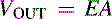

(7.1)
(7.2)
Collecting terms yields Equation (7.4):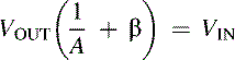
(7.4)
Rearranging terms yields the classic form of the feedback equation: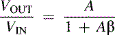
(7.5)
Note that Equation (7.5) reduces to Equation (7.6) when the quantity Aβ in Equation (7.5) becomes very large with respect to 1. Equation (7.6) is called the ideal feedback equation, because it depends on the assumption that Aβ ≫ 1; and it finds extensive use when amplifiers are assumed to have ideal qualities. Under the conditions that Aβ ≫ 1, the system gain is determined by the feedback factor, β. Stable passive circuit components are used to implement the feedback factor, thus the ideal closed loop gain is predictable and stable because β is predictable and stable.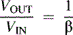
(7.6)
The quantity Aβ is so important that it has been given a special name, loop gain. Consider Figure 7.2; when the voltage inputs are grounded (current inputs are opened) and the loop is broken, the calculated gain is the loop gain, Aβ. Now, keep in mind that this is a mathematics of complex numbers, which have magnitude and direction. When the loop gain approaches −1, or to express it mathematically, 1∠−180°, Equation (7.5) approaches infinity because 1/0 ⇒ ∞. The circuit output heads for infinity as fast as it can using the equation of a straight line. If the output were not energy limited, the circuit would explode the world, but it is energy limited by the power supplies, so the world stays intact.
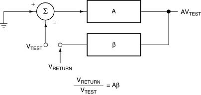 |
| Figure 7.2 Feedback loop broken to calculate the loop gain. |
Active devices in electronic circuits exhibit nonlinear behavior when their output approaches a power supply rail, and the nonlinearity reduces the amplifier gain until the loop gain no longer equals 1∠−180°. Now the circuit can do two things: First, it could become stable at the power supply limit; second, it can reverse direction (because stored charge keeps the output voltage changing) and head for the negative power supply rail.
The first state, where the circuit becomes stable at a power supply limit, is named lockup; the circuit remains in the locked up state until power is removed. The second state, where the circuit bounces between power supply limits, is named oscillatory. Remember, the loop gain, Aβ, is the sole factor that determines stability for a circuit or system. Inputs are grounded or disconnected when the loop gain is calculated, so they have no effect on stability. The loop gain criteria is analyzed in depth later.
(7.1) and (7.2) are combined and rearranged to yield Equation (7.7), which gives an indication of system or circuit error: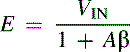
(7.7)
First, note that the error is proportional to the input signal. This is the expected result because a bigger input signal results in a bigger output signal, and bigger output signals require more drive voltage. Second, the loop gain is inversely proportional to the error. As the loop gain increases, the error decreases; thus large loop gains are attractive for minimizing errors. Large loop gains also decrease stability, so there is always a trade-off between error and stability.
7.3. Noninverting Op Amps
A noninverting op amp is shown in Figure 7.3. The dummy variable VB is inserted to make the calculations easier, and a is the op amp gain.
 |
| Figure 7.3 Noninverting op amp. |
Equation (7.8) is the amplifier transfer equation: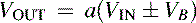
(7.8)
The output equation is developed with the aid of the voltage divider rule. Using the voltage divider rule assumes that the op amp impedance is low.
(7.9)

Rearranging terms in Equation (7.10) yields Equation (7.11), which describes the transfer function of the circuit: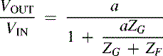
(7.11)
Equation (7.5) is repeated as Equation (7.12) to make a term by term comparison of the equations easy:
(7.12)
By virtue of the comparison, we get Equation (7.13), which is the loop gain equation for the noninverting op amp. The loop gain equation determines the stability of the circuit. The comparison also shows that the open loop gain, A, is equal to the op amp open loop gain, a, for the noninverting circuit: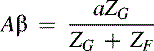
(7.13)
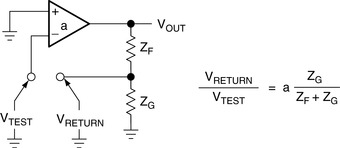
Equation (7.13) is also derived with the aid of Figure 7.4, which shows the open loop noninverting op amp.
 |
| Figure 7.4 Open loop noninverting op amp. |
The test voltage, VTEST, is multiplied by the op amp open loop gain to obtain the op amp output voltage, aVTEST. The voltage divider rule is used to calculate Equation (7.15), which is identical to Equation (7.14) after some algebraic manipulation:
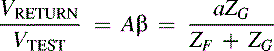
(7.14)
(7.15)
7.4. Inverting Op Amps
The inverting op amp circuit is shown in Figure 7.5. The dummy variable VA is inserted to make the calculations easier, and a is the op amp open loop gain.
 |
| Figure 7.5 Inverting op amp. |
The transfer equation is given in Equation (7.16):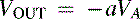
(7.16)
The node voltage, Equation (7.17), is obtained with the aid of superposition and the voltage divider rule. Equation (7.18) is obtained by combining (7.16) and (7.17).

(7.17)
(7.18)
Equation (7.16) is the transfer function of the inverting op amp. By virtue of the comparison between (7.18) and (7.14), we get Equation (7.15) again, which is also the loop gain equation for the inverting op amp circuit. The comparison also shows that the open loop gain (A) is different from the op amp open loop gain (a) for the noninverting circuit.
The inverting op amp with the feedback loop broken is shown in Figure 7.6 and this circuit is used to calculate the loop gain given in Equation (7.19):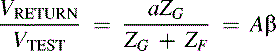
(7.19)
 |
| Figure 7.6 Inverting op amp: Feedback loop broken for loop gain calculation. |
Several things must be mentioned at this point in the analysis. First, the transfer functions for the noninverting and inverting (7.13) and (7.18), are different. For a common set of ZG and ZF values, the magnitude and polarity of the gains are different. Second, the loop gain of both circuits, as given by (7.15) and (7.19), is identical. Therefore the stability performance of both circuits is identical although their transfer equations are different. This makes the important point that stability is not dependent on the circuit inputs. Third, the A gain block shown in Figure 7.1 is different for each op amp circuit. By comparison of (7.5)(7.11) and (7.18), we see that ANONINV = a and AINV = aZF/(ZG + ZF).
7.5. Differential Op Amps
The differential amplifier circuit is shown in Figure 7.7. The dummy variable VE is inserted to make the calculations easier, and a is the open loop gain.
 |
| Figure 7.7 Differential amplifier circuit. |
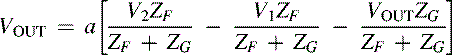
Equation (7.20) is the circuit transfer equation:
(7.20)
The positive input voltage, V+, is written in Equation (7.21) with the aid of superposition and the voltage divider rule: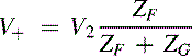
(7.21)
The negative input voltage, V–, is written in Equation (7.22) with the aid of superposition and the voltage divider rule: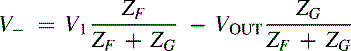
(7.22)

The comparison method reveals that the loop gain, as shown in Equation (7.25), is identical to that shown in (7.13) and (7.19):
(7.25)
Again, the loop gain, which determines stability, is a function of only the closed loop and independent of the inputs.
..................Content has been hidden....................
You can't read the all page of ebook, please click here login for view all page.