
Chapter 22. High Speed Filter Design
22.1. Introduction
Designing of high speed filters, as opposed to designing filters fast (as presented in the last chapter), represents the final frontier of active filter design. As filter operating frequencies approach higher and higher frequencies, their response begins to change in unpredictable ways, presenting the designer with an increasingly difficult design problem. Many of these effects are related to the slew rate limitation of the amplifier and begin to manifest themselves decades in frequency below the unity gain bandwidth. A 1 GHz amplifier may be limited to a few hundred kilohertz when used in a filter design. This chapter presents these limitations and shows actual examples of how successful high speed filter designs can be implemented.
22.2. High Speed, Low Pass Filters
Believe it or not, achieving low pass filter response at high speeds is very easy. All the designer has to do is to find an op amp with the correct unity gain bandwidth (or bandwidth at the gain desired). Then, the designer has to close the loop—the compensation internal to the op amp does the rest! In fact, multiple poles inside the op amp may make multiple pole, low pass filters unnecessary. A single op amp may suffice for two or more poles of low pass response.
22.3. High Speed, High Pass Filters
At high speeds, all potential high pass filter topologies are ultimately limited by the bandwidth of the op amp. Therefore, the very best scenario for a high pass filter is that it will become some kind of high pass, followed by a low pass, in other words, a wide bandpass filter. This is not to say there will be no applications where a –3 dB point for a high pass filter won't reject unwanted low frequency components, but the designer must be cognizant that, as the cutoff frequency of a high pass filter increases, it also approaches the bandwidth limitation of the op amp. Therefore, this chapter does not cover high speed, high pass filters in any great detail.
22.4. High Speed Bandpass Filters
At high speeds, all potential high pass filter topologies are ultimately limited by the bandwidth of the op amp. Obviously, limiting the number of op amps yields the highest frequency bandpass, as only one op amp limits the bandwidth. There are several single op amp bandpass filter topologies, but the most producible is a modified version of the MFB topology, also a variation of the Deliyannis. When one looks at the Deliyannis and MFB schematics side by side, in Figure 22.1, it is evident that they differ by only one resistor R3.
 |
| Figure 22.1 Deliyannis and MFB topologies. |
As is often the case in filter design, an increase in the number of components increases design flexibility. For the Deliyannis bandpass filter, if R1 = R2 = RO and C1 = C2 = CO, the center frequency is given by
Gain is –6.02 dB and Q is 0.5
However, this is only one case. As the Q of the Deliyannis filter is increased, the gain increases in an almost unbounded fashion. The designer using the Deliyannis filter has the correct value of Q but excessive gain, which also limits the usable bandwidth of the op amp. For relatively low values of Q, the Deliyannis is acceptable, but it is possible to do better.
22.4.1. Modifying the Deliyannis Topology
Consider again the special case of the Deliyannis where R1 = R2 = RO and C1 = C2 = CO. Modifying the Deliyannis filter by the addition of R3 has a curious effect. Designers used to voltage dividers are drawn visually to a voltage divider formed by R1 and R3, and assume that the gain is reduced by a factor of 2. Curiously, this is not the case. If R1 = R2 = R3 = RO, and C1 = C2 = CO, the gain is unchanged: It is still –6.02 dB. The center frequency, however, has become
The bandwidth of the filter also remains unchanged; however the change in fO has affected the Q:
Clearly, jumping to conclusions is not advisable. Doubling the value of R2 in the circuit, however, makes both the gain and Q equal to 1 and the center frequency again becomes
Redrawing the MFB portion of Figure 22.1 to resemble a modified Deliyannis filter gives us Figure 22.2.
 |
| Figure 22.2 MFB topology redrawn as modified Deliyannis filter. |
If all four resistors are made equal, center frequency, Q, and gain are unchanged from the previous example. The nice thing about this particular implementation is that center frequency fO can be adjusted independently of gain and Q by controlling the values of RO and CO. Gain and Q, however, are linked by the relationship where
where
If RQ2 is doubled, RQ1 must be halved and vice versa. If one is tripled, the other must be one third, and so on. RQ2 and RQ1 must always be related in this way. Otherwise, the center frequency is changed—and analysis of this circuit must be done with traditional MFB transfer equations.
The linking of gain and Q is not a huge disadvantage for narrow bandpass filters, as the objective is usually to detect a tone, and gain is usually desirable or at least not a tight requirement. The designer must be careful only to not drive the op amp outputs beyond the voltage rails for the maximum expected input signal level. If the tone being detected has a large dynamic range and high sensitivity is needed, that would also lead to voltage levels beyond the rails of the op amp in close proximity to the source of the tone—output limiting op amps such as the OPA688 and OPA689 should be used.
Simulating this circuit yields the family of curves for increasing gain and Q in Figure 22.3. A couple of things are apparent in the figure.
• As in all single stage bandpass filters, the ultimate roll-off slope in the stop bands is –20 dB/decade. The best way for the designer to think of this is that single stage (two pole) bandpass filters provide one pole low pass and one pole high pass filtering. Where the bandpass filter response reduces to this slope is entirely dependent on the Q value.
• The response of this filter at 100 kHz, 1 MHz, 100 MHz, and 1 GHz is (almost) unchanged for values of Q between 1 and infinity. The filter response at 10 MHz, however, goes to whatever amplitude it takes to achieve the Q value required of the circuit.
 |
| Figure 22.3 Effect of varying RQ1 and RQ2. |
These are the response characteristics inherent in the circuit of Figure 22.2. If more control is required over gain, it can be adjusted down by the addition of a voltage divider on the input. This voltage divider, of course, modifies one of the RO resistors, so the design process can get tedious. But it does give some measure of independent control over the center frequency, Q, and gain of the bandpass circuit.
22.4.2. Modified Deliyannis versus MFB
A designer might be asking at this point, “Why not just use the MFB bandpass topology as a more general solution!” This is a very reasonable question and is not trivialized here. The answer again lies in component sensitivities and past experience with MFB bandpass filters. When a general solution for an MFB filter was used to design a bandpass filter, the resulting Monte Carlo analysis again shows tremendous variation in gain, as shown in Figure 22.4.
 |
| Figure 22.4 Monte Carlo analysis of an MFB filter. |
This filter was supposed to have 17 dB of gain, yet the result of 50 runs, using 1% resistors and 2% capacitors, showed a gain variation of more than 30 dB (from 12 dB to 42 dB). Further, hidden somewhere in the amplitude response is a case where the filter does not even have a bandpass characteristic. The evidence of this is on the phase plot, where the phase of one run went exactly opposite in phase to the rest.
It is evident that, in high production volumes, the MFB approach is simply not manufacturable. Even with 2% capacitors—two amplitude plots and one phase plot showed unacceptable variation—3 runs out of 50 is a 6% failure rate.
The modified Deliyannis approach described previously gave the Monte Carlo analysis shown in Figure 22.5.
 |
| Figure 22.5 Monte Carlo analysis of a modified Deliyannis filter. |
When the two analyses are compared, the modified Deliyannis approach is far superior. It produces component values that are not as sensitive to variation as those that can be obtained from the general MFB approach.
22.4.3. Lab Results
A modified THS4271 EVM was tested at a standard bandpass frequency of 10.7 MHz to see what levels of Q could realistically be implemented. The schematic is shown in Figure 22.6.
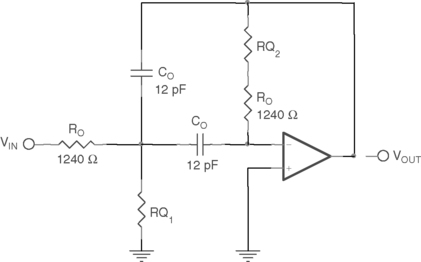 |
| Figure 22.6 10.7 MHz bandpass filter. |
The values of RQ were varied in to change the Q without affecting the center frequency. A 1% resistor sequence made it very easy to change resistors in a 1–2–5 sequence (rather than aiming for specific values of Q).
The values of RQ1 and RQ2 in Table 22.1 were used in the bandpass filter of Figure 22.6. The resulting responses are shown on the right hand set of curves in Figure 22.7.
| RQ1 | RQ2 | Resulting Q | Resulting gain (dB) |
|---|---|---|---|
| 1240 Ω | 1240 Ω | 1 | 0 |
| 619 Ω | 2490 Ω | 1.5 | 5.28 |
| 249 Ω | 6190 Ω | 3 | 9.54 |
| 124 Ω | 12.4 kΩ | 5.5 | 14.8 |
| 61.9 Ω | 24.9 kΩ | 10.5 | 20.4 |
| 24.9 Ω | 61.9 kΩ | 25.5 | 28.1 |
| 12.4 Ω | 124 kΩ | 50.5 | 34.1 |
 |
| Figure 22.7 Bandpass filter lab results. |
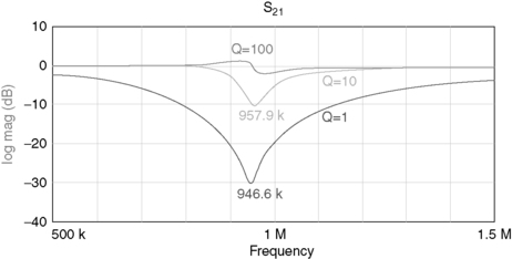
Clearly, the results show some type of problem with higher Q bandpass filters at 10.7 MHz. The center frequency shifts to the left, while the amplitude decreases. No attempt was even made to do a plot at a Q of 50.5—the plot at a Q of 25.5 was degraded so badly that the trend was clear.
The open loop response of the op amp, when superimposed on the preceding data, shows that the 10.7 MHz bandpass filters come within 30 dB of the open loop plot. There is a “truism” when working with op amps that one should have at least 40 dB of headroom above the center frequency before encountering the open loop characteristic. Nowhere is that demonstrated more dramatically than here. At a gain and Q of 1, a bandpass filter at 10.7 MHz is about 33 dB away from the open loop characteristic of the THS4271. The bandpass filter works almost correctly; the slightly low amplitude probably has more to do with real world resistor values than any sort of bandwidth limitation. But, at higher values of Q and gain, the amplitude could never rise to 10 dB. In fact, the center frequency is shifted lower as the circuit tries to compensate for the open loop response limitation.
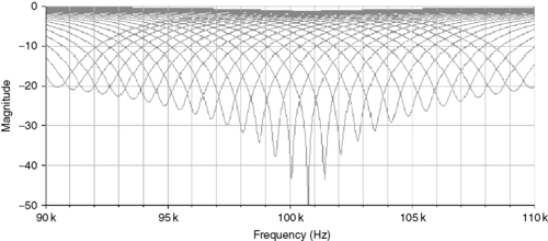
It is very easy to scale the center frequency of the filter down by a factor of 10 and 100 to change the two CO capacitors to 120 pF and 1.2 nF, respectively. This created filters centered at 1.07 MHz and 107 kHz. The results are also shown on Figure 22.7:
• Clearly, the filters centered at 1.07 MHz suffer far less from degradation at higher Q values than those at 10.7 MHz. Very little frequency shift was observed. There is, however, a limit on the amplitude to just below 20 dB, which is about 30 dB from where the open loop curve crosses 1 MHz.
• The filters centered at 107 kHz create a set of curves reminiscent of Figure 22.3, yet there is a slight degradation of amplitude at higher values of Q. Amplitude on the highest peaks is limited to about 28 dB, which is 42 dB below the open loop response at 1 MHz.
Clearly, the 40 dB headroom rule is well advised. Operating a bandpass circuit too close to the open loop response degrades first the gain and Q and finally affects the center frequency.
22.5. High Speed Notch Filter
Ordinarily, the lowest possible number of op amps would be the best for a high speed filter, and that would lead a designer to a twin T notch. This chapter does not cover the twin T notch filter topology, because it is too hard to control center frequency and Q with real world components. Instead, the more producible Fliege notch topology is used and shown in Figure 22.8.
 |
| Figure 22.8 Fliege notch filter topology. |
The advantages of this circuit over the twin T are
• Only four precision components (two R and two C) are required for tuning the center frequency. One nice feature of this circuit is that slight mismatches of components are OK—the center frequency is affected but not the notch depth.
• The Q value of the filter can be adjusted independently from the center frequency by using two noncritical resistors of the same value.
• The center frequency of the filter can be adjusted over a narrow range without seriously eroding the depth of the notch.
22.5.1. Simulations
Simulations were first performed with ideal op amp models. Real op amp models were used later, which produced results similar to those observed in the lab. Table 22.2 shows the component values that were used for the schematic of Figure 22.8. There was no point in performing simulations at or above 10 MHz, because lab tests were actually done first and 1 MHz was the top frequency at which a notch filter worked.
| 1 MHz | 100 kHz | 10 kHz | |||||||
|---|---|---|---|---|---|---|---|---|---|
| Q | RO | CO | RQ | RO | CO | RQ | RO | CO | RQ |
| 100 | 1.58 kΩ | 100 pF | 316 kΩ | 1.58 kΩ | 1 nF | 316 kΩ | 1.58 kΩ | 10 nF | 316 kΩ |
| 10 | 31.6 kΩ | 31.6 kΩ | 15.8 kΩ | 1 nF | 316 kΩ | ||||
| 1 | 3.16 kΩ | 3.16 kΩ | 31.6 kΩ | ||||||
A word about capacitors: although the capacitance is just a value for simulations, actual capacitors are constructed of different dielectric materials. For 10 kHz, resistor value spread constrained the capacitor to a value of 10 nF. While this worked perfectly well in simulation, it forced the author to change from an NPO dielectric to an X7R dielectric in the lab, with the result that the notch filter lost its characteristic completely. The 10 nF capacitors used measured close in value, so the loss of notch response was most likely due to poor dielectric. The circuit had to revert to the values for a Q of 10, and a 3 MΩ RQ was used. For real world circuits, it is best to stay with NPO capacitors.
These component values were used in both simulations and lab testing. Initially, the simulations were done without the 1 kΩ potentiometer (the two 1 kΩ fixed resistors were connected directly together and to the noninverting input of the bottom op amp). Simulation results are shown in Figure 22.9.
 |
| Figure 22.9 Simulation results before tuning. |
There are actually nine sets of results in Figure 22.9, but the curves for each Q value overlay those at the other frequencies. The center frequency in each case is slightly above a design goal that would be right on 10 kHz, 100 kHz, or 1 MHz. This is as close as a designer can get with a standard E96 resistor and E12 capacitor. Consider the 100 kHz case:
A closer combination exists if E24 sequence capacitors are available:
The inclusion of E24 sequence capacitors can lead to more accurate center frequencies in many cases, but procuring the E24 sequence values is considered an expensive (and unwarranted) expenditure in many labs. While it may be easy to specify E24 capacitor values in theory, in practice many of them are seldom used and have long lead times associated with them.
There are easier alternatives to selecting E24 capacitor values. Close examination of Figure 22.9 shows that the notch “misses” the center frequency by only a small amount. At lower Q values, there is still substantial rejection of the desired frequency. If the rejection is not sufficient, then it becomes necessary to tune the notch filter.
Again considering the 100 kHz case, the response near 100 kHz is spread out on Figure 22.10. The 1 kΩ potentiometer is inserted and adjusted up and down in 1% steps.
 |
| Figure 22.10 Tuning for center frequency. |
The family of curves to the left and right of the center frequency (100,731 Hz) represents the filter response when the potentiometer is adjusted in 1% increments. When the potentiometer is exactly in the middle, the notch filter rejects frequencies at the exact center frequency. The depth of the simulated notch is actually on the order of 95 dB, but that is not going to happen in the real world. A 1% adjustment of the potentiometer puts a notch that is greater than 40 dB right on the desired frequency. Again, this is best case with ideal components, but lab results are close at low frequencies (10 kHz and 100 kHz).
Figure 22.10 shows that it is important to get close to the correct frequency, starting with RO and CO. While the potentiometer can correct for frequency over a broad range, the depth of the notch degrades. Over a small range (±1%), it is possible to get a 100:1 rejection of the undesirable frequency. But over a larger range (±10%), it is possible to get only a 10:1 rejection.
22.5.2. Lab Results
A THS4032 evaluation board was used to construct the circuit of Figure 22.8. Its general purpose layout required only three jumpers and one trace cut to complete the circuit. The components of Table 22.2 were used, starting with the components that would produce 1 MHz. It was the intention to look for bandwidth and slew rate restrictions at 1 MHz and test at lower or higher frequencies as necessary.
22.5.3. 1 MHz Results
Figure 22.11 shows that there are some very definite bandwidth or slew rate effects at 1 MHz. The response at a Q of 100 shows barely a ripple on the response curve where the notch should be. At a Q of 10, there is only a 10 dB notch, and a 30 dB notch at a Q of 1. Apparently, notch filters cannot achieve as high a frequency as hoped. But the THS4032 is only a 100 MHz device; it is reasonable to expect better performance from parts with a greater unity gain bandwidth. Unity gain stability is important, because the Fliege topology has fixed unity gain.
 |
| Figure 22.11 1 MHz lab results. |
If the designer wishes to estimate what bandwidth is required for a notch at a given frequency, a good place to start is the published gain and bandwidth product, which should be 100 times the center frequency of the notch. Additional bandwidth is required for higher Q values. There is a slight frequency shift of the notch center frequency as Q is changed. This is similar to the frequency shift seen for bandpass filters. The frequency shift is less for notch filters centered at 100 kHz (Figure 22.12) and 10 kHz (Figure 22.13).
 |
| Figure 22.12 100 kHz lab results. |
 |
| Figure 22.13 Tuning for exact center frequency. |
22.5.4. 100 kHz Results
Component values from Table 22.2 were then used to create 100 kHz notch filters with different Q values. The results are shown in Figure 22.12. It is immediately obvious that viable notch filters can be constructed with center frequency of 100 kHz, although the notch depth appears to be less at higher values of Q.
Remember, though, that the design goal in this section is a 100 kHz notch, not a 97 kHz notch. The component values selected are the same as the simulation, so the notch center frequency should theoretically be at 100,731 Hz, but the difference is explained by the parts in the lab. The mean value of the 1000 pF capacitor stock was 1030 pF and that of the 1.58 kΩ resistor stock was 1.583 kΩ. When the center frequency is calculated with these values, it comes out to 97.14 kHz. The actual components, however, could not be measured (the board was too fragile).
As long as the capacitors are matched, it would be possible to go up a couple of standard E96 resistor values to get closer to 100 kHz. Of course, this is probably not an option in high volume manufacturing, where 10% capacitors could come from any batch and potentially from different manufacturers. The range of center frequencies is determined by the tolerances of RO and CO, which is not good news if a high Q notch is required. There are three ways of handling this:
• Purchase higher precision resistors and capacitors.
• Lower the Q requirement and live with less rejection of the unwanted frequency.
• Tune the circuit (which is explored next).
At this point, the circuit was modified to have a Q of 10, and a 1 kΩ potentiometer was added for tuning the center frequency (as shown in Figure 22.8). In real world design, the value of the potentiometer should be selected to slightly more than cover the range of center frequencies possible with worst case RO and CO tolerances. That was not done here, as this was an exercise in determining possibilities; and 1 kΩ was the lowest potentiometer value available in the lab.
When the circuit was tuned for a center frequency of 100 kHz, as shown in Figure 22.13, the notch depth degraded from 32 dB to 14 dB. Remember that this notch depth could be greatly improved by making the initial fO closer to ideal. The potentiometer is meant to tune over only a small range of center frequencies. Still, a 5:1 rejection of an unwanted frequency is respectable and may be sufficient for some applications. More critical applications will obviously need higher precision components.
It may also be true that bandwidth limitations from the op amp are keeping the notch depth from being as low as possible, which also degrades the tuned notch depth. With this in mind, the circuit was retuned for a center frequency of 10 kHz.
22.5.5. 10 kHz Results
Figure 22.14 shows that the notch depth for a Q of 10 increased to 32 dB, which is about what one would expect from a center frequency 4% off from simulation (Figure 22.9). The op amp was indeed limiting the notch depth at a center frequency of 100 kHz! The 32 dB is a rejection of 40:1, which is quite good.
 |
| Figure 22.14 10 kHz lab results. |
So, even with components that produced an initial 4% error, it is possible to produce a 32 dB notch at the desired center frequency. The bad news is that, to escape op amp bandwidth limitations, the highest notch frequency possible with a 100 MHz op amp is somewhere between 10 kHz and 100 kHz. So in the case of notch filters, high speed is defined as being somewhere in the tens or hundreds of kilohertz.
Note: Some artistic liberties were taken on this plot. The laboratory instrument displays only down to 10 kHz, so the left hand portion of the plot is a mirror image of the right hand portion. Also, the laboratory instrument has some roll-off at frequencies below 100 kHz, which were artistically eliminated from this plot.
A good application for 10 kHz notch filters is AM (medium wave) receivers, where the carrier from adjacent stations produces a loud 10 kHz whine in the audio, particularly at night. This is a real earful and can really grate on one's nerves when listening for a prolonged time. Figure 22.15 shows the received audio spectrum of a station before and after the 10 kHz notch was applied. In this case, the 10 kHz carrier interference is shown as a string of peaks that vary in amplitude. When the notch is applied, the 10 kHz peaks are eliminated, and there is only a slight ripple in the received audio where 10 kHz has been notched out.
 |
| Figure 22.15 Effect of heterodyning and the notch filter. |
For European readers who want to have a more pleasing medium wave listening experience, the component values are these:
Shortwave listeners benefit from a two stage notch filter, one section being the 10 kHz described previously and the other stage being a 5 kHz notch filter with these component values:
22.6. Conclusions
High speed op amps have been used to produce low pass and high pass filters up to the tens of megahertz with fairly good success. Narrow bandpass filters and notch filters are much less understood and much more critical applications. While the tolerance of a capacitor might change the cutoff frequency of a low pass filter or produce ripple in the passband, that same tolerance can produce dramatic changes in center frequency and Q of bandpass and notch filters.
..................Content has been hidden....................
You can't read the all page of ebook, please click here login for view all page.