
Chapter 21. Fast, Practical Filter Design for Beginners
21.1. Introduction
The previous chapter presented a rigorous theoretical approach to filter design. Many designers prefer this method because it gives the most flexibility in filter design. Years of customer support, however, have revealed that the vast majority of designers want a working filter with the minimum effort and development time. This chapter presents a pragmatic, simple design methodology that allows a designer to implement all but the most complex filters rapidly and have a reasonable expectation that they will be producible.
To design a filter, these things must be known in advance:
• The frequencies that need to be passed and those that need to be rejected.
• A transition frequency, the point at which the filter starts to work or a center frequency around which the filter is symmetrical.
• An initial capacitor value—pick one somewhere from 100 pF for high frequencies to 0.1 μF for low frequencies. If the resulting resistor values are too large or too small, pick another capacitor value.
21.2. Picking the Response
For the beginner, the filter responses are presented pictorially in Figure 21.1Figure 21.2Figure 21.3Figure 21.4Figure 21.5 and Figure 21.6. The shaded area represents the frequencies that will be passed, and the area in white the frequencies that will be rejected. Don't be concerned with the exact frequency yet, that will be taken care of in the following sections.
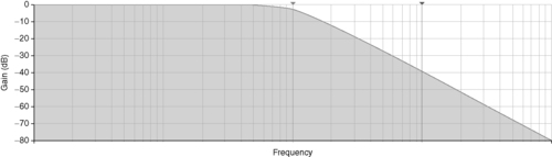 |
| Figure 21.1 Low pass response, go to Section 21.3. |
 |
| Figure 21.2 High pass response, go to Section 21.4. |
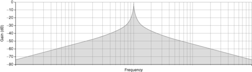 |
| Figure 21.3 Narrow (single frequency) bandpass, go to Section 21.5. |
 |
| Figure 21.4 Wide bandpass, go to Section 21.6. |
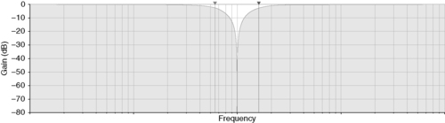 |
| Figure 21.5 Notch (single frequency rejection) filter, go to Section 21.7. |
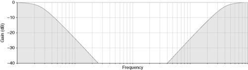 |
| Figure 21.6 Wide band rejection, go to Section 21.8. |
21.3. Low Pass Filter
Figure 21.7 shows a low pass filter.
 |
| Figure 21.7 Low pass filter. |
The design procedure is as follows:
• Pick C1: __________
• Calculate C2 = C1 × 2: __________
• Calculate R1 and R2 =  : __________
• Calculate CIN = COUT = 100 to 1000 times C1 (not critical): __________
Done!
Digging deeper, the filter selected is a unity gain Sallen-Key filter, with a Butterworth response characteristic. Note that, with the addition of CIN and COUT, the filter is no longer purely a low pass filter. It is a wide bandpass filter, but the high pass response characteristic can be placed well below the frequencies of interest. If DC response is required, the circuit should be modified to operate off of split supplies.
21.4. High Pass Filter
Figure 21.8 shows a high pass filter.
 |
| Figure 21.8 High pass filter. |
The design procedure is as follows:
• Pick C1 = C2 = __________
• Calculate  ___________
• Calculate  __________
• Calculate COUT = 100 to 1000 times C1 (not critical) = __________
Done!
Digging deeper, the filter selected is a unity gain Sallen-Key filter, with a Butterworth response characteristic. Just as was the case with the low pass filter, there is no such thing as an active high pass filter—but for a different reason. The gain and bandwidth product of the op amp used ultimately produces a low pass response characteristic, making this a wide bandpass filter. It is the responsibility of the designer to choose an op amp with a frequency limit well above the bandwidth of interest.
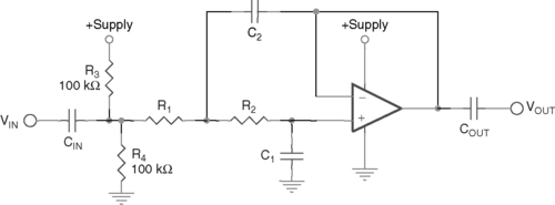
21.5. Narrow (Single Frequency) Bandpass Filter
Figure 21.9 shows a narrow bandpass filter.
 |
| Figure 21.9 Narrow bandpass filter. |
The design procedure is as follows:
• Pick C1 = C2 = __________
• Calculate R1 = R4 =  = ___________
• Calculate R3 = 19 × R1
• Calculate R2 = R1/19
• Calculate CIN = COUT = 100 to 1000 times C1 (not critical) = __________
Done!
Digging deeper, the filter selected is a modified Deliyannis filter. A Deliyannis filter is a special case of the MFB bandpass configuration, one that is very stable and relatively insensitive to component variation. The Q is set at 10, which also locks the gain at 10, as the two are related by the expression
A higher Q was not selected, because the op amp gain bandwidth product can be easily reached, even with a gain of 20 dB. At least 40 dB of headroom should be allowed above the center frequency peak. The op amp slew rate should also be sufficient to allow the waveform at the center frequency to swing to the amplitude required.
Digging even deeper, we look at the narrow versus wide bandpass filter (Figure 21.10). At what point is it better to implement a bandpass filter as a narrow or single frequency filter versus a wide bandpass? At high Q values, the single frequency bandpass is clearly the better choice. However, as Q values decrease, the difference begins to blur. What can be a very sharp peak at resonance erodes to a single pole roll-off on the low end and single pole roll-off on the high end. This results in a lot of unwanted energy in the stop bands.
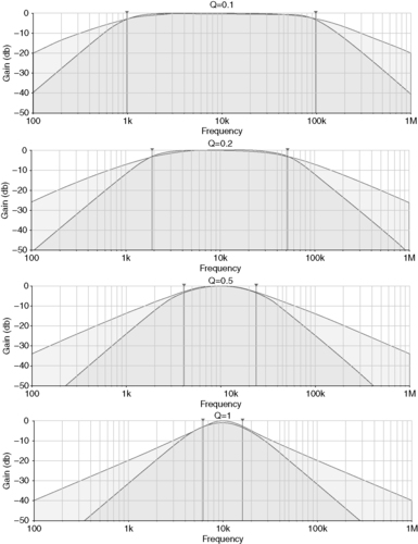 |
| Figure 21.10 Narrow versus wide bandpass filter. |
Clearly, for Q values of 0.1 (and below) and 0.2, the best implementation is high pass cascaded with low pass. The lighter shaded regions correspond to a large amount of energy in the stop bands not rejected with a bandpass filter. In the wide passband, the cascaded approach is also clearly superior, because there is a wider region in the passband where response is flat.
The two implementations have almost an identical pass band response for a Q of 0.5. The designer is presented with a choice—use a bandpass filter (which can be implemented with a single op amp) to save money or use a cascaded approach that has better rejection in the stop bands.
As the Q becomes higher and higher, however, the responses of two separate stages begin to interact, destroying the amplitude of the signal. The designer at this point can still opt for the cascaded approach if stop band rejection is the primary concern and amplitude response is secondary. Amplitude response begins to degrade badly for even higher values of Q, however, ending the usefulness of the cascaded approach.
A good rule of thumb is that the starting and ending frequencies of the band should be at least five times different.
21.6. Wide Bandpass Filter
Figure 21.11 shows a wide bandpass filter.
 |
| Figure 21.11 Wide bandpass filter. |
The design procedure is as follows:
• Go to Section 21.3 and design a high pass filter for the low end of the band.
• Go to Section 21.2, and design a low pass filter for the high end of the band.
• Calculate CIN = COUT = 100 to 1000 times C1 in the low pass filter section (not critical) = __________.
Done!
Digging deeper, we find this is nothing more than cascaded Sallen-Key high pass and low pass filters. The high pass comes first, so noise from it will be low passed.
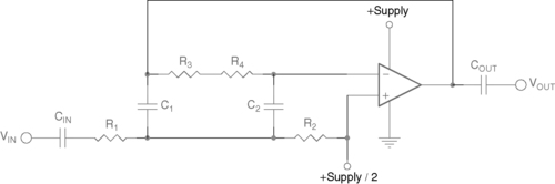
21.7. Notch (Single Frequency Rejection) Filter
Figure 21.12 shows a notch (single frequency rejection) filter.
 |
| Figure 21.12 Notch filter. |
The design procedure is as follows:
• Pick C1 = C2 = __________
• Calculate  ___________
• Calculate R1 = R2 = 20 × R3.
• Calculate CIN = COUT = 100 to 1000 times C1 (not critical): __________
Done!
Digging deeper, we find this is the Fliege filter topology, set to a Q value of 10. The Q can be adjusted independently from the center frequency by changing R1 and R2. Q is related to the center frequency set resistor by the following: 
The Fliege filter topology has a fixed gain of 1.
Many designers use the “twin T” notch topology for notches. While it is a popular topology, it has many problems. The biggest is that it is not producible. Many runs of simulation with component tolerances of 1% have shown tremendous variation in notch center frequency and notch depth. The only real advantage is that it can be implemented with a single op amp. Some additional stability can be obtained from the two op amp configuration, but if two op amps are used, then why not use a different topology, such as the Fliege? To successfully use the twin T topology, six precision components are required. The Fliege produces a deep null at some frequency, and it is easy to tune that frequency by adjusting one of the resonance resistors—the null will remain as deep over a fairly wide range. R5 and R6 are the only critical elements, they don't have to be 100 k, they can be scaled together, but they should be matched.
We dig even deeper. Just as was the case with the narrow bandpass filter versus the wide bandpass filter, a decision must be made about whether it is better to implement a notch filter or a band reject filter. Figure 21.13 shows the transition between the two types of filter.
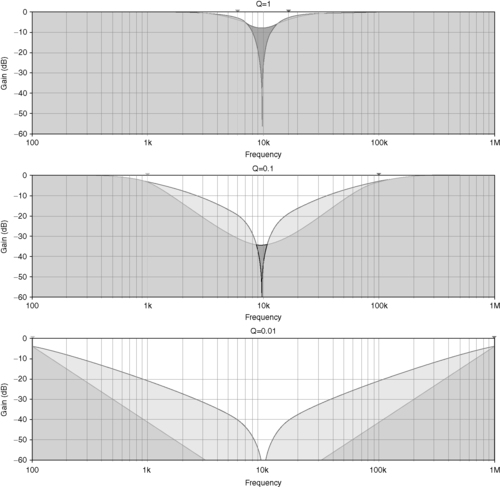 |
| Figure 21.13 Notch filter versus wide band reject filter. |
Even with Q as low as 1, it is clearly better to use a notch filter for a single frequency. But for lower Q values, more and more unwanted energy is passed by a notch filter than a band reject filter. A good rule of thumb for using a band reject filter is that the starting and ending frequencies of the band to be rejected should be at least 50 times different.
21.8. Band Reject Filter
Figure 21.14 shows a band reject filter.
 |
| Figure 21.14 Band reject filter. |
The design procedure is as follows:
• Go to Section 21.3, and design a high pass filter for the low end of the upper band.
• Go to Section 21.2, and design a low pass filter for the high end of the lower band.
• For the single supply case only, calculate CIN = COUT = 100 to 1000 times C1 in the low pass filter section (not critical): __________.
Done!
Digging deeper, we find this is nothing more than summed Sallen-Key high pass and low pass filters. They cannot be cascaded, because their responses do not overlap as in the wide bandpass filter case.
21.9. Summary of Filter Characteristics
Table 21.1 gives a summary of the various filter types and the cost of implementing them.
..................Content has been hidden....................
You can't read the all page of ebook, please click here login for view all page.