
Chapter 17. Using Op Amps for RF Design
17.1. Introduction
RF design used to be the exclusive domain of discrete devices. The advent of new generations of high speed voltage and current feedback op amps made it possible to use op amps for RF design. Op amp based RF circuitry is easier to design and has less associated risk. “Tweaking” in the lab can be almost eliminated. Despite the many advantages, traditional RF designers are reluctant to utilize op amps. They are confronted with a bewildering array of op amp parameters, many of which do not relate directly to the set of design parameters with which they are familiar. This chapter bridges the gap between RF designers and op amp designers, giving RF designers common ground with which to begin their design.
When talking about using op amps for RF design, the question that has to be answered is, Why? Traditional RF design techniques, using discrete transistors, have been practiced successfully for decades. RF designers who are comfortable with things “as is” scrutinize introduction of a new design technique, using op amps. The cost of high speed op amps, in particular, raises eyebrows. Why replace a transistor, which costs a few cents, with a component that may cost several dollars?
This is a valid question to ask for high volume consumer goods, and in almost every case, the answer is to stay with traditional techniques. For high performance RF equipment, however, high speed op amps have some distinct advantages. History has shown than many other applications have migrated to op amps in the past to take advantage of the superior performance they provide. It is reasonable to assume that high speed applications such as RF will also make the move.
17.2. Advantages
The first major advantage is flexibility. High speed op amps offer a high degree of flexibility over discrete transistor implementations. When discrete transistors are used, the bias and operating point of the transistor interacts with the gain and tuning of the stage.
In contrast, when op amps are used, the bias of the stage is accomplished simply by applying the appropriate power supplies to the op amp power pins. Gain of the stage is completely independent of the bias. Gain does not affect the tuning of the stage, which is accomplished through passive components.
Transistor parameter drift must also be taken into account over the system operating temperature range. When op amps are used, the drift is reduced.
17.3. Disadvantages
As attractive as op amps are for RF design, some barriers hinder their use. The first barrier, of course, is cost.
The RF designer must learn how to set the op amp's operating point, but the process is considerably easier than biasing a transistor stage.
The RF designer is used to describing RF performance in certain ways. Analog designers think in terms of AC performance. The two ways of thinking are not compatible. The RF designer must learn how to translate op amp AC performance parameters into an RF context. That is one of the main purposes of this chapter.
17.4. Voltage Feedback or Current Feedback?
The RF designer considering op amps is presented with a dilemma: Are voltage feedback amplifiers or current feedback amplifiers better for the design? Frequency of operation is usually the most demanding aspect of RF design, and this makes the op amp bandwidth a critical parameter. The bandwidth specification given in op amp data sheets refers only to the point where the unity gain bandwidth of the device has been reduced by 3 dB by internal compensation or parasitics, which is not very useful for determining the actual operating frequency range of the device in an RF application.
Internally compensated voltage feedback amplifier bandwidth is dominated by an internal “dominant pole” compensation capacitor. This gives them a constant gain/bandwidth limitation. Current feedback amplifiers, in contrast, have no dominant pole capacitor and therefore can operate much closer to their maximum frequency at higher gain. Stated another way, the gain/bandwidth dependence has been broken.
To illustrate this, a voltage feedback and current feedback op amp are compared:
• THS4001, a voltage feedback amplifier with a 270 MHz (−3 dB) open loop bandwidth, is usable to only about 10 MHz at a gain of 10 (20 dB).
• THS3001, a current feedback amplifier with a 420 MHz (−3 dB) open loop bandwidth, is usable to about 150 MHz at a gain of 10 (20 dB).
It is still the call of the designer to determine what he or she wants to do. At unity and low gains, there may not be much advantage to using a current feedback amplifier, but at higher gains, the choice is clearly a current feedback amplifier. Many RF designers would be extremely happy if they could obtain a gain of 10 (20 dB) in a single stage with a transistor—it is difficult to do. With an op amp, it is almost trivial.
17.5. A Review of Traditional RF Amplifiers
A traditional RF amplifier (Figure 17.1) uses a transistor (or, in the early days, a tube) as the gain element. DC bias (+VBB) is injected into the gain element at the load through a bias resistor RB. RF is blocked from being shorted to the supply by an inductor LC, and DC is blocked from the load by a coupling capacitor.
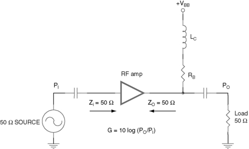 |
| Figure 17.1 A traditional RF stage. |
Both the input impedance and the load are 50 Ω, which ensures matching between stages.
When an op amp is substituted as the active circuit element, several changes are made to accommodate it.
By themselves, op amps are differential input, open loop devices. They are intended to be operated in a closed loop topology (different from a receiver's AGC loop). The feedback loop for each op amp must be closed locally, within the individual RF stage.
There are two ways of accomplishing this. The op amp designer refers to them as inverting and noninverting. These terms refer to whether the output of the op amp circuit is inverted from the input or not. From the standpoint of RF design, this is seldom of any concern. For all practical purposes, either configuration works and gives equivalent results.
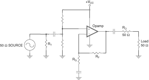
Figure 17.2 shows a noninverting RF amplifier. The input impedance of the noninverting input is high, so the input is terminated with a 50 Ω resistor. Gain is set by the ratio of RF and RG: For a desired gain,
 |
| Figure 17.2 Noninverting RF op amp gain stage. |
The gain of this stage as shown should never be below one half (−6 dB), because most op amps are unity gain stable.
The output of the stage is converted to 50 Ω by placing a 50 Ω resistor in series with the output. This, combined with a 50 Ω load, means that the gain is divided by 2 (−6 dB) in a voltage divider. So, a unity gain (0 dB) gain stage would become a gain of one half, or −6 dB.
The RF designer may note that the power supply requirements have been complicated by the addition of a second negative supply. The stage can be modified easily for single supply operation, as shown in Figure 17.3.
 |
| Figure 17.3 Single supply noninverting RF amplifier. |
A virtual ground is generated on the noninverting input after the coupling capacitor, to raise the operating point of the op amp to a virtual ground halfway between the supply voltage and ground.
Coupling capacitors are needed to isolate preceding and succeeding stages and the gain resistor RG from the virtual ground DC potential. These capacitors should be selected to have low impedance at the operating frequency, but not so small that they affect the gain of the stage directly or cause unacceptable variations in gain over the operating range of the stage.
If the amplifier selected is a voltage feedback type, it is also possible to make an inverting RF stage. Inverting stages made from current feedback amplifiers are not generally practical because of the low input impedance of the inverting input, which is connected to the output of an internal voltage buffer.
Figure 17.4 shows an inverting RF amplifier. The input impedance of this configuration is still relatively high and is again terminated with a 50 Ω resistor. Gain is set by the ratio of RF and RG.
 |
| Figure 17.4 Inverting RF stage. |
The output of the stage is converted to 50 Ω by placing a 50 Ω resistor in series with the output. This is combined with a 50 Ω load, which means that the gain is divided in 2 (6 dB) in a voltage divider. An inverting stage must be used for gains less than one half, or −6 dB, again because most op amps are unity gain stable. For a desired gain,
As before, the RF designer may notice that the power supply requirements have been complicated by the addition of a second negative supply. As before, it can be modified easily for single supply operation, as shown in Figure 17.5.
 |
| Figure 17.5 Single supply inverting RF amplifier. |
A virtual ground is generated on the noninverting input to raise the operating point of the op amp to a virtual ground halfway between the supply voltage and ground. This virtual ground should be local to the stage and decoupled locally to prevent RF emission or conduction out of the stage. It is unwise to produce a virtual ground to use in more than one stage because of the possibility of crosstalk.
Coupling capacitors are needed to isolate preceding and succeeding stages from the virtual ground DC potential. These capacitors should be selected to have low impedance at the operating frequency, as before.
17.6. Amplifier Gain Revisited
Op amp designers think of the gain of an op amp stage in terms of voltage gain. RF designers, in contrast, are used to thinking of RF stage gain in terms of power:
17.7. Scattering Parameters
RF stage performance is often characterized by four “scattering” parameters, which are defined in Table 17.1.
The term scattering has a certain implication of loss, and that is indeed the case in three cases. Reflections, as in the VSWR (voltage standing wave ratio) scattering parameters S11 and S22, can cancel useful signals. Reverse transmission, S12, steals output power from the load. The only desirable scattering parameter is S21, the forward transmission. Design of an RF stage involves maximizing S21 and minimizing S11, S22, and S12.
Small signal AC parameters specified for RF amplifiers are derived from S parameters. These specifications are frequency dependent. They are measured using a network analyzer and an S parameter test set. The test circuit is shown in Figure 17.6.
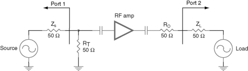 |
| Figure 17.6 Scattering parameter test circuit. |
17.7.1. Input and Output VSWR S11 and S22
The voltage standing wave ratio is just another term for input or output reflection. It is a ratio, and therefore a unitless quantity. VSWR is a measure of how well the input and output impedances are matched to the source and load impedances. They should be as closely matched as possible to avoid reflections.
VSWR is defined as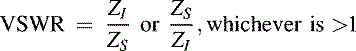 where
where
ZI = amplifier input or output impedance.
ZS = test system source impedance.
The ideal VSWR is equal to 1:1, but typical VSWR's are no better than 1.5:1 for RF amps over their operating frequency range.
Measuring the input VSWR is a matter of measuring the ratio of the reflected power versus incident power on Port 1 of the previous figure (S11). A perfect match reflects no power. Output VSWR is measured the same way at Port 2 (S22).
An op amp's input and output impedances are determined by external components selected by the designer. For this reason, VSWR cannot be specified on an op amp's data sheet.
17.7.2. Return Loss
Return loss is related to VSWR in the following way: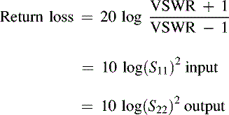
RO is not a perfect match for ZL at high frequencies. The output impedance of the amplifier increases as the loop gain falls off. This changes the output VSWR. A peaking capacitor, CO, added in parallel with RO can compensate for this effect. Because op amp output impedance is well defined, a fixed value can usually be substituted after experimentation determines the correct value (Figure 17.7).
 |
| Figure 17.7 Output peaking capacitor. |
The termination resistor sets the input impedance, but as the frequency increases, nonresistive effects come into play. Not only do the effects of the termination resistor come into effect, but those of RG and RF as well. Figure 17.8 illustrates the high frequency model of a stage.
 |
| Figure 17.8 Simplified high frequency inverting stage. |
Obviously, analysis of a high frequency stage can become a nightmare. Using microwave components reduces these parasitic effects and extends the maximum usable frequency of the circuit. Reducing the input impedance of the amplifier also extends the maximum usable frequency by swamping the effects of high frequency parasitic components.
There are three ways of reducing the input impedance:
• Use the inverting configuration with a voltage feedback amplifier.
• Use the noninverting configuration with a current feedback amplifier.
• Limit the gain of the stage.
17.7.3. Forward Transmission S21
The forward transmission, S21, is specified over the operating frequency range of interest. S21 is never specified on an op amp data sheet, because it is a function of the gain, which is set by the input and feedback resistors, RF and RG. The forward transmission of a noninverting op amp stage is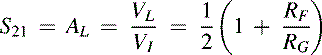
The forward transmission of an inverting op amp stage is
Op amp data sheets show open loop gain and phase. It is the responsibility of the designer to know the closed loop gain and phase. Fortunately, this is not hard to do. The data sheets many times include excellent graphs of open loop bandwidth and sometimes include phase. Closing the loop produces a straight line across the graph at the desired gain, curving to meet the limit. The open loop bandwidth plot should be used as an absolute maximum. The designer that approaches the limit does so at the expense of extensive compensation and complex PCB layout techniques.
To illustrate this point, two hypothetical 1 GHz op amps are shown in Figure 17.9, one voltage feedback and the other current feedback. If a gain of 20 dB is required, the voltage feedback amplifier is limited to just over 10.7 MHz, barely adequate for an FM IF amplifier. If a gain of 40 dB is required, the voltage feedback amplifier is limited to just over 1 MHz, barely adequate for medium wave/AM amplification.
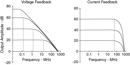 |
| Figure 17.9 Gain bandwidth comparison of voltage and current feedback op amps. |
The current feedback amplifier, on the other hand, is usable to about 50 MHz in both cases. The designer is cautioned to take extra care to avoid oscillations at high gains. Remember the RF designer's rule: All oscillators begin as amplifiers, and all amplifiers begin as oscillators.
17.7.4. Reverse Transmission S12
Op amp topologies, in particular current feedback amplifiers, assume both inputs are connected to low impedances. Therefore, the reverse isolation of op amp RF circuits is excellent (Figure 17.10).
 |
| Figure 17.10 Reverse transmission. |
The reason why op amps have such good reverse isolation is that, instead of the gain element being a single transistor with its associated leakage, the reverse signal has to go through the leakage of dozens or hundreds of transistors fabricated on the silicon of the op amp (Figure 17.11).
 |
| Figure 17.11 Reverse transmission path through op amps. |
Reverse isolation is somewhat better in noninverting current feedback amplifier configurations, because the output signal must also leak through the circuitry connecting the noninverting and inverting inputs to get to the source.
17.8. Phase Linearity
Oftentimes, a designer is concerned with the phase response of an RF circuit. This is particularly the case with video design, which is a specialized type of RF design. Current feedback amplifiers tend to have better phase linearity than voltage feedback amplifiers:
• Voltage feedback THS 4001: Differential phase = 0.15°.
• Current feedback THS 3001: Differential phase = 0.02°.
17.9. Frequency Response Peaking
Current feedback amplifiers allow an easy resistive trim for frequency peaking that has no impact on the forward gain. This frequency response flatness trim has the same effect in noninverting and inverting configurations.
Figure 17.12 shows this adjustment added to an inverting circuit. This resistive trim inside the feedback loop has the effect of adjusting the loop gain, hence the frequency response, without adjusting the signal gain, which is still set by RF and RG.
 |
| Figure 17.12 Frequency response peaking. |
Values for RF and RG must be reduced to compensate for the addition of the trim potentiometer, although their ratio and hence the gain should remain the same. The adjustment range of the potentiometer, combined with the lower RF value, ensures that the frequency response can be peaked for slight current feedback amplifier parameter variations.
17.10. −1 dB Compression Point
The −1 dB compression point is defined as the output power, at a fixed input frequency, where the amplifier's actual output power is 1 dBm less than expected. Stated another way, it is the output power at which the actual amplifier gain has been reduced by 1 dB from its value at lower output powers. The −1 dB compression point is the way RF designers talk about voltage rails.
Op amp designers and RF designers have very different ways of thinking about voltage rails, which are related to the requirements of the systems that they design:
• An op amp designer interfacing op amps to data converters, for example, takes great pain not to hit the voltage rail of the op amp, thus losing precious codes.
• An RF designer, on the other hand, is often concerned with squeezing the last half decibel out of an RF circuit. In broadcasting, for example, a very slight increase in decibels means a lot more coverage. More coverage means more audience and more advertising dollars. Therefore, slight clipping is acceptable, as long as the resulting spurs are within FCC regulations.
Standard AC coupled RF amplifiers show a relatively constant −1 dB compression power over their operating frequency range. For an operational amplifier, the maximum output power depends strongly on the input frequency. The two op amp specifications that serve a similar purpose to −1 dB compression are VOM and slew rate.
At low frequencies, increasing the power of a fixed frequency input eventually drives the output “into the rails,” the VOM specification. At high frequencies, op amps reach a limit on how fast the output can transition (respond to a step input). This is the slew rate limitation of the amplifier. The op amp slew rate specification is divided by 2, because of the matching resistor used at the output.
As is the case for op amps used in any other application, it is probably best to avoid operation near the rails, as the inevitable distortion produces harmonics in the RF signal—harmonics that are probably undesirable for FCC testing. That said, if harmonics are still at an acceptable level at the −1 dB compression point, it can be a very useful way to boost power to a maximum level out of the circuit.
17.11. Two Tone, Third Order Intermodulation Intercept
When two closely spaced signals are present in the RF bandwidth being amplified, sum and difference frequencies are created. These sum and difference frequencies are intermodulation harmonics. They are undesirable and may lead to problems with FCC testing of the system.
The problem with these harmonics is that they increase in amplitude three times as fast as the fundamentals. Figure 17.13 shows a theoretical system with a beginning fundamental signal level of 0 dBM, with intermodulation harmonics at −60 dBm. As the amplitude of the fundamentals is increased, the harmonics are seen increasing at three times the rate of the fundamentals, leading to an eventual intercept of the two lines at +30 dBm.
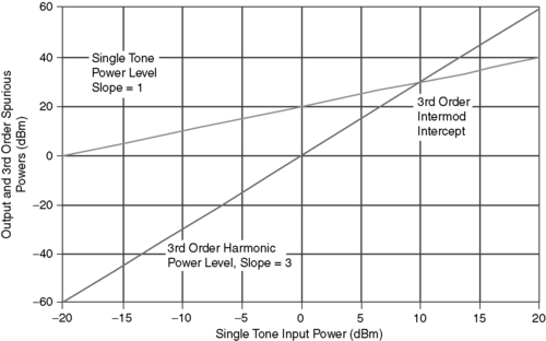 |
| Figure 17.13 Two tone, third order intermodulation intercept. |
The typical RF circuit can not be adjusted to +30 dBm, so the third order intermodulation intercept is theoretical. The third order intermodulation intercept should be as high as possible, because that means that the intermodulation harmonics are proportionally lower at any real world fundamental level.
Figure 17.14 demonstrates the two tone intermodulation intercept in a different way. The fundamental frequencies at fO − Δf and fO + Δf are shown, so are the third order harmonics at fO − 3Δf and fO + 3Δf. While the fundamentals are raised a total of 30 dBm, the harmonics increase 90 dBm, eventually attaining the same amplitude as the fundamentals! Clearly, this must be avoided in a working RF system if spurs are to be rejected at all.
 |
| Figure 17.14 Two tone, third order intermodulation intercept amplitudes. |
17.12. Noise Figure
The RF noise figure is the same thing as op amp noise, when an op amp is the active element. There is some effect from thermal noise in resistors used in RF systems, but the resistor values in RF systems are usually so small that their noise can be ignored.
Noise for an op amp RF circuit is dependent on the bandwidth being amplified and gain.
This example assumes the  op amp. The application is a 10.7 MHz IF amplifier. The signal level is 0 dBV. The gain is unity.
Figure 17.15 is extrapolated from real data. The 1/f corner frequency, in this case, is much lower than the bandwidth of interest. Therefore, the 1/f noise can be completely discounted (assuming that filtering removes any noise that would cause the amplifier or data converter to saturate). For narrow bandwidths, noise may be quite low! Various bandwidths are shown in Table 17.2.
 |
| Figure 17.15 Noise bandwidth. |
| Bandwidth | EIN | SNR |
|---|---|---|
| 280 kHz | 6.09 μV | −104.3 dB |
| 230 kHz | 5.52 μV | −105.2 dB |
| 180 kHz | 4.88 μV | −106.2 dB |
| 150 kHz | 4.45 μV | −107.0 dB |
| 110 kHz | 3.81 μV | −108.4 dB |
| 90 kHz | 3.45 μV | −109.4 dB |
Obviously, a slight advantage is to be had from reducing the bandwidth. A lower noise op amp, however, provides greater benefit.
Noise is amplified by the gain of the stage. Therefore, if a stage has high gain, care must be taken to find a low noise op amp. If the gain of a stage is lower, then the noise is not amplified as much, and a less expensive op amp may be suitable.
17.13. Conclusions
Op amps are suitable for RF design, provided that the cost can be justified. They are more flexible to use than discrete transistors, because the biasing of the op amp is independent of the gain and termination. Current feedback amplifiers are more suitable for high frequency, high gain RF design, because they do not have the gain/bandwidth limitation of voltage feedback op amps.
Scattering parameters for RF amplifiers constructed with op amps are very good. Input and output VSWR are good because the effects of termination and matching resistors can be made independent of stage biasing. Reverse isolation is very good, because the RF stage is made of an op amp consisting of dozens or hundreds of transistors, instead of a single transistor. Forward gain is very good with a current feedback amplifier.
Special considerations apply to RF designs that do not normally apply to op amp designs: the phase linearity; the −1 dB compression point (as opposed to voltage rails); the two tone, third order intermodulation intercept; peaking; and noise bandwidth. In just about every case, the performance of an RF stage implemented with op amps is better than one implemented with a single transistor.
..................Content has been hidden....................
You can't read the all page of ebook, please click here login for view all page.