
Chapter 25. Common Application Mistakes
25.1. Introduction
When one works as an analog applications engineer for many years supporting customer inquiries, some patterns begin to emerge. Inquires run the gamut from newcomers who have no business attempting analog design to those from analog design experts who encountered something new and unusual that challenges even the best support engineer. Unfortunately, there is also a class of inquiries that are bound to elicit a groan, mistakes the author has seen many times before and unfortunately will see many times again. It is hoped that this chapter will educate people to some of the most common mistakes and save designers from continuing to make them.
25.2. Op Amp Operated at Less than Unity (or Specified) Gain
Does the phrase unity gain stable ring a bell? In early chapters of this book, the statement was made that an op amp is least stable at its lowest specified gain. Ideally, the engineer has read the material and understands the true nature of stability, and yet, during the book tour for the first edition of this book, a customer approached me with a problem: This person had a programmable gain op amp circuit where resistors were switched to program a gain of 1, 1/10, and 1/100 (see Figure 25.1). The unity gain case worked as expected, but ringing occurred with a gain of 1/10 and sustained oscillation at a gain of 1/100. In no way do I demean the individual who made this mistake; I have been known to grab an amplifier out of a bin to construct a quick circuit, only to have it oscillate uncontrollably. Invariably, a quick glance at the data sheet reveals it is a “gain of ten” stable op amp not unity gain stable. There is no other option at that point but to use a different op amp.
 |
| Figure 25.1 Op amp attenuator done wrong. |
Fortunately, the solution to the problem is exceptionally easy. A voltage divider can be applied to the input of a noninverting op amp buffer, as shown in Figure 25.2.
 |
| Figure 25.2 Op amp attenuator done correctly. |
As far as the op amp is concerned, it is operating at unity gain and is stable. The voltage divider rule is employed to calculate the correct degree of attenuation. The high input impedance of the noninverting op amp input does not affect the voltage divider to any degree unless extremely large value resistors are used.
If the signal must be inverted, then the inverting attenuator of Figure 25.3 can be used. It is a variation on the approach used in Figure 25.2 but takes into account the resistors used for the op amp feedback and input resistance.
 |
| Figure 25.3 Inverting op amp attenuator. |
Texas Instruments has a calculator available on its Web site to assist in the calculation.
A common objection to the solution of Figure 25.2 is that it introduces resistor noise to the attenuator. This is a fallacy for two reasons—first of all, the incorrect inverting attenuator also contains resistors that are going to be almost the same value. The second reason is that the carbon composition resistors that caused the problem are a fast fading memory. Most resistors now are metal film or thick film types that have much better noise specifications.
25.3. Op Amp Used as a Comparator
This misapplication usually occurs in cost sensitive pieces of equipment when a comparator is needed and a quad op amp has an unused section. I first encountered it when I discovered that the expensive telephone answering machine I had purchased quit working. “Why?” I asked myself, “is there an open loop op amp circuit on one quarter of an LM324, and why is it interfaced to a digital logic gate?” The answer was that somebody looked at the schematic symbol of an op amp and the schematic symbol of a comparator (Figure 25.4), saw that they look alike, and decided that they both work the same way!
 |
| Figure 25.4 Similar schematic symbols, very different parts! |
Unfortunately, not even the internal schematic of the parts give much indication of what is going on (see Figure 25.5 and Figure 25.6).
 |
| Figure 25.5 Example op amp schematic. |
 |
| Figure 25.6 Example comparator schematic. |
The input stages look almost identical, except the inputs have opposite labels (a fine point discussed later). The output stage of the op amp is a bit more complex, which should be a clue that something is different. The output stage of the comparator is obviously different, in that it is a single open collector. But be careful—many newer comparators have bipolar stages that are very similar in appearance to op amp output stages.
So, if very little appears to be different in the schematic symbol or the internal workings, what is the difference? The difference is in the output stage. An op amp has an output stage optimized for linear operation, while the output stage of a comparator is optimized for saturated operation.
25.3.1. The Comparator
A comparator is a 1 bit analog to digital converter. It has a differential analog input and a digital output. Very few designers make the mistake of using a comparator as an op amp, because most comparators have open collector output. The output transistor of open collector comparators is characterized by low VCE for switching heavy loads. The open collector structure depends on external circuitry to make the connection to power and complete the circuit. Some comparators also bring out the emitter pin as well, relying on the designer to complete the circuit by making both collector and emitter connections. Other comparators substitute an FET, having open drain outputs instead of open collector. The emphasis is on driving heavy loads.
The comparator is an open loop device, utilizing no feedback resistors. When applying a comparator, the designer compares the voltage level at two inputs. The comparator produces a digital output that corresponds to the inputs:
• If the voltage on the noninverting (+) input is greater than the voltage on the inverting (–) input, the output of the comparator goes to low impedance “on” for open collector/drain outputs and “high” for totem pole outputs.
• If the voltage on the noninverting (+) input is less than the voltage on the inverting (–) input, the output of the comparator goes to high impedance “off” for open collector/drain outputs and “low” for totem pole outputs.
25.3.2. The Op Amp
An op amp is an analog component with a differential analog input and an analog output. If an op amp is operated open loop, the output seems to act like a comparator output, but is this a good thing to do?
An op amp, being intended for closed loop operation, is optimized for closed loop applications. The results are unpredictable when an op amp is used open loop. No semiconductor manufacturer can or will guarantee the operation of an op amp used in an open loop application. The analog output transistors used in op amps are designed for the output of analog waveforms and therefore have large linear regions. The transistors spend an inordinate amount of time in the linear region before saturation, making the rise and fall times lengthy.
In some cases, the designer may get away with using an op amp as a comparator. When an LM324 is operated in this fashion, it hits a rail and stays there, but nothing “bad” happens. The situation can change dramatically, however, when another device is substituted.
The design of an op amp output stage is bad news for the designer who needs a comparator with fast response time. The transistors used for op amp output stages are not switching transistors. They are linear devices, designed to output accurate representation of analog waveforms. When saturated, they not only may consume more power than expected, they may also latch up. Recovery time may be very unpredictable. One batch of devices may recover in microseconds, another batch in tens of milliseconds. Recovery time is not specified, because it cannot be tested. Depending on the device, it may not recover at all! Runaway destruction of the output transistors is a distinct possibility in some rail to rail devices. Even the best designer might produce a saturated or even open loop op amp circuit without realizing it.
Oh, why did my answering machine fail? The Vol rail of the open loop op amp circuit created was above the logic threshold of the digital gate to which it was interfaced. The two levels were very close—and the slightest drift upward of the op amp output stage caused the low logic threshold to never be reached. Vol is yet another op amp specification that will never be specified under open loop conditions.
25.4. Improper Termination of Unused Sections
One of the easiest ways to unintentionally misapply an op amp is to misapply unused sections of a multiple section IC. Figure 25.7 shows the most common ways designers connect unused sections.
 |
| Figure 25.7 Different ways of dealing with unused op amp sections. |
Many designers know how to properly terminate unused digital inputs, hooking them to the supply or ground. These designers may not have a clue how to terminate unused op amps. Figure 25.7 demonstrates techniques of Texas Instruments applications actually seen. I gave them titles:
• Brain dead. This is a common mistake. Designers will assume an op amp is like an audio amp at home and just leave unused inputs unconnected. This is the absolute worst thing that can be done to an op amp. An open loop op amp saturates to one voltage rail or the other. Because the inputs are floating—and picking up noise—the output of the op amp switches from rail to rail, sometimes at unpredictable high frequencies.
• Never. This is another really bad thing that designers occasionally do. Usually, one op amp input is slightly higher than the other due to ground plane gradients, and the best possible scenario is that the op amp will saturate at one rail or the other. There is no guarantee it will stay there, as a slight change on one pin could cause it to switch to the other rail.
• No. This is a little better than the previous case but not that much. All the designer has accomplished is to ensure that the op amp will hit a rail—and stay there. This can wreak havoc—self-heating, increased power consumption.
• Just as bad. Designers who are designing a board for in circuit test commonly do this. It still makes the op amp hit a rail.
• Good. This is the minimum recommended circuit configuration. The noninverting input is tied to a potential between the positive and negative rail or to ground in a split supply system. Virtual ground may already exist in the system, making the resistors unnecessary. The op amp output also is at virtual ground (or ground in a split supply system).
• Smart. The smart designer anticipates the possibility of system changes in the future and lays out the board so that the unused op amp section could be used by changing resistors and jumpering. The schematic shows how the unused section could be used for either an inverting or noninverting stage, as required.
25.5. DC Gain
Another way designers create problems is when they forget about DC components on AC signals. Figure 25.8 illustrates this problem. When an AC signal source has a DC offset, a coupling capacitor isolates the potential in the top circuit. The DC component is rejected, and output voltage is 1 VAC. If the coupling capacitor is omitted, the circuit attempts a gain of –10 on both the AC and DC components, which would be 1 VAC, –50 VDC. Because the power supply of the circuit limits the DC output to ±15 VDC, the output will be saturated at –15 VDC (minus the voltage rail limitation of the op amp).
 |
| Figure 25.8 Unexpected DC gain. |
25.6. Current Source
The op amp current source circuit shown in Figure 25.9must always contain the load. Many applications put the load at the end of a cable, and the cable is on a connector. When the cable is unplugged, the op amp has positive feedback! It will hit the negative voltage rail.
 |
| Figure 25.9 Current source. |
The output of the current source is 


It should be understood that R1 through R4 are much greater than R5, and R5 ≫ RLOAD.
25.7. Current Feedback Amplifier: Shorted Feedback Resistor
By far the most common mistake with current feedback amplifiers occurs when a designer shorts the output directly to the inverting input, as in Figure 25.10.
 |
| Figure 25.10 Current source with shorted output. |
The designer is invariably trying to take advantage of the speed and bandwidth of the CFB to create a buffer. Shorting the output pin to the inverting input is always a bad idea, because it makes the CFB unstable. Stability criteria for the current feedback amplifier are different from that of the voltage feedback amplifier. The voltage feedback amplifier stability criterion is 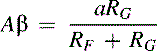
The current feedback amplifier stability criterion is 
As you can see, VFB stability depends equally on both RF and RG. But CFB stability is much more dependent on RF. In fact, if RF is zero, the denominator goes to zero and the stability criterion fails! This is seen graphically in actual data sheet plots (Figure 25.11).
 |
| Figure 25.11 VFB versus CFB stability versus load resistor. |
The effect of changing RF only slightly has an enormous effect on the CFB response on the left, with an alarming trend as the resistor is lowered. The effect is much smaller and opposite with the VFB plot on the right. The bottom line is this: Stick with the recommended value of feedback resistor for CFB op amps. That also makes a very easy solution when a noninverting buffer is desired. Just put the recommended value of feedback resistor between the output and inverting input, and the stage will work perfectly!
25.8. Current Feedback Amplifier: Capacitor in the Feedback Loop
A capacitor often ends up in the feedback loop when the designer is attempting to do active filter design with CFAs (Figure 25.12).
 |
| Figure 25.12 Capacitor in the feedback loop. |
Very few filter topologies work with CFAs. The Sallen-Key is one—if the proper value of feedback resistor is employed. The bottom line is that CFAs are not the best choice for active filter designs. Choose something else wherever possible.
25.9. Fully Differential Amplifier: Incorrect Single Ended Termination
One of the most common applications for a fully differential op amp is single ended to fully differential conversion. However, when the input signal must be terminated, the situation gets very complicated!
Looking at the circuit in Figure 25.13 and the equations that govern it, R1 and Rt are cross defined. Solving this equation for the correct values requires a goal seeking algorithm. If the values are calculated incorrectly, the results can be
• Wrong gain.
• Differential offset.
• Unmatched differential gain.
• Incorrect matching impedance.
 |
| Figure 25.13 Terminating a fully differential amplifier. |
Fortunately for the designer, Texas Instruments provides a calculator on its Web site to do this task automatically.
The designer might want to consider the simpler design alternative in Figure 25.14.
 |
| Figure 25.14 Using an input stage. |
25.10. Fully Differential Amplifier: Incorrect DC Operating Point
Single supply operation of a fully differential amplifier is very easy to mess up (just see Figure 25.15).
 |
| Figure 25.15 Incorrect DC operating point. |
What happened? The two outputs have a 3.3 VDC difference between their operating points! Remember that differential input circuits have two potential sources of DC. In this case, the designer correctly put an AC coupling capacitor between V1 and R1 but forgot to put one between R3 and ground. Figure 25.16 shows what happens when the second AC coupling capacitor is installed.
 |
| Figure 25.16 Correct DC operating point. |
When the second AC coupling capacitor is inserted, the correct DC operating point is established.
25.11. Fully Differential Amplifier: Incorrect Common Mode Range
A very subtle but equally destructive problem often arises from incorrect application of the VOCM input of the fully differential amplifier when the amplifier frequency response has to include DC, making AC coupling capacitors impossible. Consider the circuit in Figure 25.17.
 |
| Figure 25.17 Common mode error. |
The DC operating point appears to be correctly established, the outputs will swing around the VOCM common mode point, which is established at 5 V by V3. But, when an AC simulation is done, the results are terrible. What happened?
The problem comes when the input voltage range does not include the negative rail, in this case, ground. There are two solutions for the problem. One is to offset the inputs to the same DC level as VOCM. The other is to choose a fully differential amplifier that includes the negative rail in its common mode range. Figure 25.18 illustrates the effect of VOCM on the output signals.
 |
| Figure 25.18 The effects of VOCM on outputs. |
VOCM causes problems when it forces the outputs of the amplifier too close to the power supply rails. It is best to operate both inputs and VOCM as close as possible to the same DC potential.
25.12. The Number 1 Design Mistake
I saved the very best and most common mistake for last. And it doesn't even involve an op amp. It involves support components: the decoupling capacitors!
In Chapter 1, I mentioned some part numbers that are etched in the memory of every design engineer, at least those involved in analog design. There is one other: 0.1 μF.
Need to decouple? OK, everybody knows you put a 0.1 μF capacitor on every power supply input and the job is done, right? I can disprove that truism very easily with two words: cell phone.
Put your cell phone near your prototype circuit, which is bypassed with 0.1 μF, and make a call while monitoring the output on a high bandwidth oscilloscope. You will see horrendous 2.4 GHz leakage!
An alternative version of this problem came from some cellular telephone base station installers who called in a panic, “We have 90 MHz noise running all over our system—and can't figure out where it is coming from.” A suspicion on my part asked them to tell me the exact coordinates where they were installing the system, and they provided the exact latitude and longitude. A quick check of the FCC database revealed the problem. I asked them, “Are you anywhere near the tower for W____ 90.5 FM, a 100,000 W NPR station listed at those coordinates?” They told me on the phone that they could see the transmitter 5 ft away—they were colocating with the station!
The point of this is that their board was bypassed with 0.1 μF capacitors. While that worked fine for the digital portions of the board, the analog portions were being clobbered by radiation of the powerful 90.5 MHz FM station. Conventional thinking is that the lower the value of capacitance, the lower the frequencies it will filter. So, 0.1uF should get rid of just about everything because it is a very large value (relatively speaking). This conventional wisdom is wrong! The actual case is the exact opposite.
Where did the value 0.1 μF come from, anyway? A high technology store near me used to have antiquated computer boards as a wall decoration. Backlit with white light, the translucent green boards made a pretty sight. But, they were also populated with 0.1 μF decoupling capacitors. A quick survey of the circuitry revealed that the clock rate of the old computer had been 1 MHz.
So, the 0.1 μF capacitor value seems to have come from bypassing TTL logic in the 1960s! Isn't it time to rethink the issue a bit, in light of op amps and other analog components that can operate to frequencies of 3 GHz, especially when almost every engineer carries a 2 W, 2.4 GHz transmitter into the lab (cell phone)?
The reality of the situation is that a good 0.1 μF capacitor with an X7R dielectric exhibits a resonance in the 10 MHz region. This is due to parasitic inductance creating an LC circuit. Below 10 MHz, its impedance is capacitive, decreasing almost linearly on a logarithmic plot until it reaches the resonant frequency. Above the resonant frequency, the impedance is inductive. Since inductor resists the flow of high frequencies and passes only low frequencies, the decoupling capacitor is useless above its resonant frequency.
Looking at representative plots from capacitor manufacturers, at 100 MHz, the venerable 0.1 μF bypass capacitor has become an inductor with an XL of at least 1 Ω. By 2.4 GHz, XL has risen to above 10 Ω.
A good rule of thumb for effective bypassing is to put several capacitors in parallel. The standard 0.1 μF capacitor does quite nicely for frequencies up to 10 MHz, a 1000 pF NPO dielectric does nicely up to 100 MHz, and 33 pF NPO eliminates frequencies in the 2.4 GHz region. Bulk decoupling of the power supply as it enters the board eliminates low frequency ripple.
Here is a truism to replace the older one: When poor decoupling is suspected, decrease (do not increase) the value of the capacitance.
..................Content has been hidden....................
You can't read the all page of ebook, please click here login for view all page.