
Appendix A. Single Supply Circuit Collection
Bruce Carter
A.1. Introduction
This chapter is devoted to a collection of single supply op amp circuits. These are presented here because they are somewhat unusual and do not fit well into the material presented in the main portion of the book.
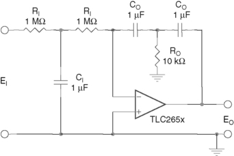
A.2. Instrumentation Amplifier
In the circuit configuration in Figure A.1, both sources connect to the noninverting input of two op amps. This impedance is very high, and if the op amps are identical, both impedances are very nearly equal. This is ideal for interfacing to very high impedance input signals. The propagation delay is equal to two op amp propagation delays, but the propagation delay is very nearly equal, so any distortion resulting from unequal propagation delays is minimized.
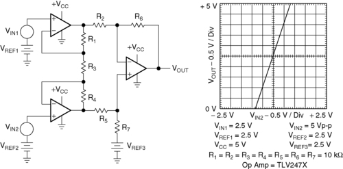 |
| Figure A.1 High precision differential amplifier. |
When R7 = R6, R5 = R2, R1 = R4, and VREF1 = VREF2, Equation (A.1) reduces to Equation (A.2): 
(A.1)
(A.2)
The equal resistors should be matched with more precision than is expected from the circuit. Resistor matching eliminates distortion due to unequal gains, and it reduces the common mode voltage feed through. Resistors equal to (R1‖R3)/2 may be placed in series with the sources to reduce errors resulting from bias currents. This differential amplifier has the unique feature that the gain can be changed with only one resistor, and if the gain setting resistor is R3, no resistor matching is required to change gain.
A.3. Simplified Instrumentation Amplifier
As shown in Figure A.2, both input sources are loaded equally with very high impedances in the simplified instrumentation amplifier. This configuration eliminates three resistors, two of which are matched, but it sacrifices flexibility in gain setting capability because the gain must be set with a matched pair of resistors.
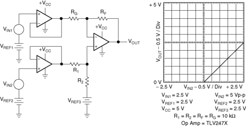 |
| Figure A.2 Simplified high precision differential amplifier. |
When RF is set equal to R2, RG is set equal to R1, and VREF1 = VREF2, Equation (A.3) reduces to Equation (A.4): 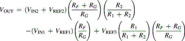
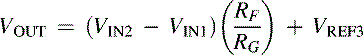
(A.3)
(A.4)
A.4. T Network in the Feedback Loop
Sometimes, it is desirable to have a low resistance path to ground in the feedback loop. Standard inverting op amps cannot do this when the driving circuit sets the input resistor value and the gain specification sets the feedback resistor value. Inserting a T network in the feedback loop (Figure A.3) yields a degree of freedom that enables both specifications to be met with a low DC resistance path to ground in the feedback loop: 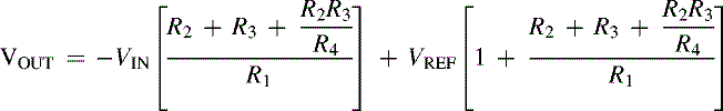
(A.5)
 |
| Figure A.3 T network in the feedback loop. |
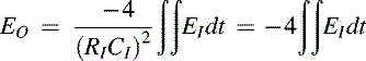
A.5. Inverting Integrator
The Laplace operator, s = jω, is used in Equation (A.6) and the mathematical operation 1/s constitutes an integration. Differentiation circuits are shown later, and the mathematical operation, s, constitutes a differentiation. The integration time constant is RC, thus the magnitude crosses 0 dB on a log plot when RC = 1. Also the phase is –45 ° when RC = 1: 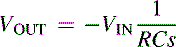
(A.6)
This integrator, shown in Figure A.4, is not very practical because there is no method of discharging the capacitor; hence any current leakage eventually charges the capacitor until the circuit becomes saturated. The positive input of the integrator is biased at VCC/2 to center the output voltage at VCC/2, thus allowing for positive and negative voltage swings. The bias resistors are selected as 2R so that the parallel combination equals R. This offsets the input current drawn through R.
 |
| Figure A.4 Inverting integrator. |
A.6. Inverting Integrator with Input Current Compensation
Functionally, the circuit in Figure A.5 is the same as that shown in Figure A.4, but a current compensation network has been added to offset the input current. VCC, R1, and R2 bias the positive input at VCC/2 to center the output voltage at VCC/2, thus allowing for positive and negative voltage swings.
 |
| Figure A.5 Inverting integrator with input current compensation. |
R1 and R2 are selected as relatively small values, because the current flowing through RA also flows through the parallel combination of R1 and R2. RA forward biases the diode with a constant current, so the diode acts like a small voltage regulator. The diode voltage drop is temperature sensitive, and this factor works in our favor because the input transistors are temperature sensitive. The two temperature sensitivities cancel out if the diode current is selected correctly. RB is a large value resistor that acts like a current source, so it is selected such that it supplies the input bias current. Selecting RB correctly ensures that no input current flows through the integration resistor, R.
This integrator is not very practical, because there is no method of discharging the capacitor. Hence, any input current eventually charges the capacitor until the circuit becomes saturated. The bias circuit drastically reduces the input current flowing through R, thus it extends the integration time. A reset circuit is needed to make the integrator more practical.
This bias compensation scheme is set up for an op amp that has npn input transistors. The diode must be reversed and connected to ground for op amps with pnp input circuits. 
(A.7)
A.7. Inverting Integrator with Drift Compensation
Functionally, the circuit in Figure A.6 is the same as that shown in Figure A.5, but it uses an RC circuit in the positive lead to obtain drift compensation. The voltage divider is made from a series string of resistors (RA), and VCC biases the input in the center of the power supply.
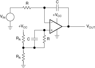 |
| Figure A.6 Inverting integrator with drift compensation. |
Positive input current flows through R and C in parallel, so the positive input current drops the same voltage across the parallel RC combination as the negative input current drops across its series RC combination. The common mode rejection capability of the op amp rejects the voltages caused by the input currents. Much longer integration times can be achieved with this circuit, but when the input signal does not center around VCC/2, the compensation is poor. 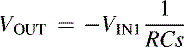
(A.8)
A.8. Inverting Integrator with Mechanical Reset
Functionally, the circuit in Figure A.7 is the same as that shown in Figure A.5, but a method has been provided to discharge (reset) the capacitor. S1 is a mechanical switch or relay; and when the contacts close, they short the integrating capacitor, forcing it to discharge. Some capacitors are sensitive to fast discharge cycles, so RS is put in the discharge path to limit the initial discharge current. When RS is absent from the circuit, the impulse of current that occurs at the first instant of discharge causes considerable noise, so the selection of RS is also based on noise considerations. For all practical purposes, the time constant formed by RS and C determines the discharge rate.
 |
| Figure A.7 Inverting integrator with mechanical reset. |
One advantage of mechanical discharge methods is that they are isolated from the remainder of the circuit. Their size, weight, time delay, and uncertain actuating time offset this advantage. When the disadvantages of mechanical reset outweigh the advantages, circuit designers go to electronic reset circuits. 
(A.9)
A.9. Inverting Integrator with Electronic Reset
Functionally, the circuit in Figure A.8 is the same as that shown in Figure A.5, but an electronic method has been provided to discharge (reset) the capacitor. Q1 is controlled by a gate drive signal that changes its state from on to off. When Q1 is on, the gate source resistance is low, less than 100 Ω. And when Q1 is off, the gate source resistance is high, about several hundred megaohms.
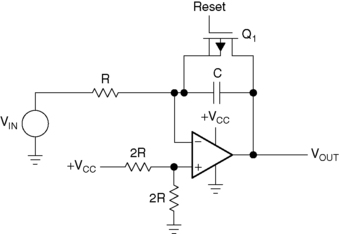 |
| Figure A.8 Inverting integrator with electronic reset. |
The source of the FET is at the inverting lead that is at ground, so the Q1 gate source bias is not affected by the input signal. Sometimes, the output signal can get large enough to cause leakage currents in Q1, so the designer must take care to bias Q1 correctly. Consult a transistor book for more detailed information on transistor reset circuits. A major problem with electronic reset is the charge injected through the transistor's stray capacitance. This charge can be large enough to cause integration errors. 
(A.10)
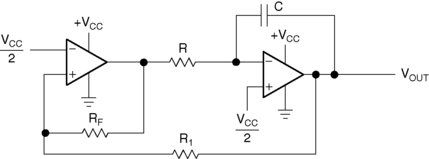
A.10. Inverting Integrator with Resistive Reset
The circuit in Figure A.9 differs from that shown in Figure A.5, because it yields a break point rather than a pure integration. On a log plot, the integrator slope is –6 dB per octave at the 0 frequency intercept, and the 0 dB intercept occurs when f = 1/2πRC. A break point plots flat on a log plot until the break point, where it breaks down at –6 dB per octave. It is –3 dB when f = 1/2πRC.
 |
| Figure A.9 Inverting integrator with resistive reset. |
RF is in parallel with the integrating capacitor, C, so it is continually discharging C. The low frequency attenuation that is the best attribute of the pure integrator is sacrificed for the reset circuit complexity. 
(A.11)
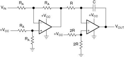
A.11. Noninverting Integrator with Inverting Buffer
The circuit in Figure A.10 is an inverting integrator preceded by an inverting buffer. Eliminating the signal inversion costs an op amp and four resistors, but this is the easiest way to get true noninverting integrator performance. 
(A.12)
 |
| Figure A.10 Noninverting integrator with inverting buffer. |
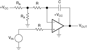
A.12. Noninverting Integrator Approximation
The circuit in Figure A.11 has fewer parts than the noninverting integrator with inverting buffer (Figure A.10), but it is not a true integrator because there is a zero in the transfer equation. The log plot starts rolling off at a –6 dB per octave rate at low frequencies, but when f = 1/2πRC, the zero cuts in. The zero causes the log plot to flatten out because the slope decreases to 0 dB per decade.
 |
| Figure A.11 Noninverting integrator approximation. |
This circuit functions as an integrator at very low frequencies, but at frequencies higher than f = 1/2πRC, it functions as a buffer. 
(A.13)
A.13. Double Integrator
 |
| Figure A.12 Double integrator. |
The double integrator integrates twice with one amplifier.
A.14. Differential Integrator
The circuit in Figure A.13 shows a differential integrator. 
(A.15)
 |
| Figure A.13 Differential integrator. |
The differential integrator integrates the difference between two signals.
A.15. AC Integrator
The circuit in Figure A.14 shows an AC integrator, which Integrates only the AC component.
 |
| Figure A.14 AC integrator. |
A.16. Augmenting Integrator
The circuit in Figure A.15 sums the input signal and its time integral: 
(A.16)
 |
| Figure A.15 Augmenting integrator. |
A.17. Inverting Differentiator
In Figure A.16, the log plot of the differentiator is a positive slope of 6 dB per octave passing through 0 dB at f = 1/2πRC. At extremely high frequencies, the capacitive reactance goes to very low values, thus the circuit gain approaches the op amp open loop gain. This performance emphasizes any system noise or noise generated by the op amp. The poor noise performance of this circuit limits its application to a very few specialized situations.
 |
| Figure A.16 Inverting differentiator. |
This configuration has a pole in the feedback loop. If the op amp has more than one pole, and most op amps have several poles, this configuration can become oscillatory. The VCC and RA circuit bias the output in the center of the power supplies. RA/2 should be selected equal to RG‖RF so that input currents are canceled out. 
(A.17)
A.18. Inverting Differentiator with Noise Filter
The circuit in Figure A.17 has a pure differentiator that rises at a 6 dB per octave slope from zero frequency. At f = 1/2πRFCF, the pole kicks in and the slope is reduced to zero. The pole has two effects. First, it stabilizes the circuit by canceling zero's phase shift. Second, it limits the circuit gain to 1 at high frequencies, so it acts like a noise filter.
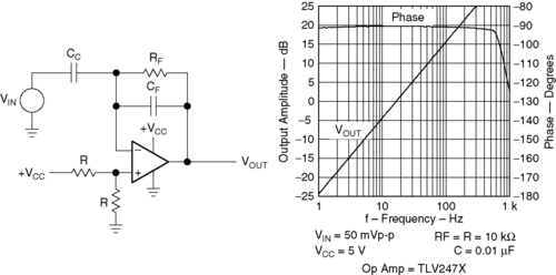 |
| Figure A.17 Inverting differentiator with noise filter. |
R/2 should equal RF for good input current cancellation, and VCC coupled with R centers the output voltage.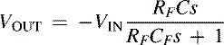
(A.18)
A.19. Augmented Differentiator
The circuit in Figure A.18 shows an augmented differentiator, which sums the input and its derivative.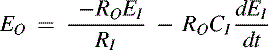
(A.19)
 |
| Figure A.18 Augmented differentiator. |
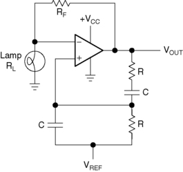
A.20. Basic Wien Bridge Oscillator
The circuit in Figure A.19 shows a basic Wien bridge oscillator. When ω = 2πf = 1/RC, the feedback is in phase (this is positive feedback) and the gain is 1/3, so oscillation requires an amplifier with a gain of 3. When RF = 2RG, the amplifier gain is 3 and oscillation occurs at f = 1/2πRC. Normally, the gain is larger than 3 to ensure oscillation under worst case conditions.
 |
| Figure A.19 Basic Wien bridge oscillator. |
VREF sets the output DC voltage in the center of the span.
The output sine wave is highly distorted because limiting by saturation and cutoff controls the output voltage excursion. The distortion decreases when the gain is decreased, but the circuit may not oscillate under worst case low gain conditions. 
(A.20)
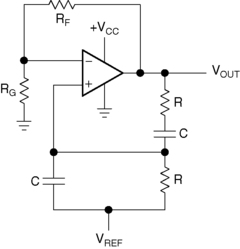
A.21. Wien Bridge Oscillator with Nonlinear Feedback
The circuit in Figure A.20 shows a Wien bridge oscillator with nonlinear feedback. When the circuit gain is 3, RL = RF/2.
 |
| Figure A.20 Wien bridge oscillator with nonlinear feedback. |
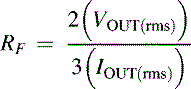
Substituting a lamp (RL) for the gain setting resistor reduces distortion, because the nonlinear lamp resistance adjusts the gain to keep the output voltage smaller than the power supply voltage. The output voltage never approaches the power supply rail, so distortion doesn't occur. RF and RL determine the lamp current, see (A.21) and (A.22):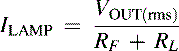
(A.21)
(A.22)
The lamp is selected by examining lamp resistance curves until a lamp with a resistance approximately equal to RF/2 at IOUT(rms) is found. The output voltage swing should be less than 75% of the maximum guaranteed voltage swing, and 3RL must be greater than the load resistance specified for the voltage swing specification. VREF should be VCC/5.
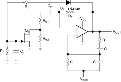
A.22. Wien Bridge Oscillator with AGC
In Figure A.21, the op amp is configured as an AC amplifier to ease biasing problems. The gain equation for the op amp follows. RG1 or RG2, but not both resistors, is required depending on the selection of the Q1. 
(A.23)
 |
| Figure A.21 Wien bridge oscillator with AGC. |
The diode, D1, half wave rectifies the output voltage and applies it to the voltage divider formed by R1 and R2. The voltage divider biases Q1 in its linear region, and they eventually set the output voltage. C1 filters the rectified sine wave with a long time constant, so that the output voltage stays constant. C2 must be selected large enough to act as a short at the oscillation frequency.
As the output voltage increases, the negative voltage across the gate of Q1 increases. The increased negative gate voltage causes Q1 to increase its drain to source resistance. This results in increased op amp gain and an output voltage decrease. When the voltage divider and FET are selected properly, the output voltage swing is less than the guaranteed maximum swing, so distortion doesn't occur.
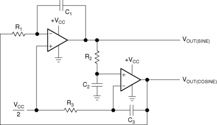
A.23. Quadrature Oscillator
Quadrature oscillators (Figure A.22) produce sine waves 90 ° out of phase, so they output sine/cosine, or quadrature waves.
 |
| Figure A.22 Quadrature oscillator. |
When R1C1 = R2C2 = R3C3, the circuit oscillates at ω = 2πf = 1/RC. Both op amps act as integrators, causing two poles at 1/RC, therefore the circuit oscillates when the loop gain crosses the 0 dB axis. The integrators ensure that gain is always sufficient for oscillation. There is a slight bit of distortion at the sine output, and it is very hard to eliminate this distortion.
A.24. Classical Phase Shift Oscillator
Theoretically, the three RC sections in Figure A.23 do not load each other, therefore the loop gain has three identical poles multiplied by the op amp gain.
 |
| Figure A.23 Classical phase shift oscillator. |
The loop phase shift is –180 ° when the phase shift of each section is –60 °, and this occurs when ω = 2πf = 1.732/RC, because the tangent of 60 ° = 1.73. The magnitude is (1/2)3, so the gain, A = RF/RG, must be greater than or equal to 8 for the system gain to be equal to 1.
The assumption that the RC sections do not load each other is not entirely valid, therefore the circuit does not oscillate at the specified frequency and the gain required for oscillation is more than 8. This circuit configuration was very popular when an active component was large and expensive; but now that op amps are inexpensive, small, and come in quad packages, the classical phase shift oscillator is losing popularity.
The classical phase shift oscillator has an undistorted sine wave available at the output of the third RC section. This is not a low impedance output, and the signal amplitude is smallest here, but these sacrifices have to be made to get away from distortion. An undistorted output can be obtained from the op amp by employing an AGC circuit similar to the one shown in Figure A.21. The reference voltage is set according to the equation VREF = VCC/(1 + RF/RG) to center the output voltage at VCC/2. 
(A.24)
A.25. Buffered Phase Shift Oscillator
A noninverting op amp buffers each RC section in the oscillator in a buffered phase shift oscillator. Equation (A.25) represents the transfer function of this circuit if RG ≫ R: 
(A.25)
The loop phase shift is –180 ° when the phase shift of each section is –60 °, and this occurs when ω = 2πf = 1.732/RC, because the tangent 60 ° = 1.73. The magnitude of β at this point is (1/2)3, so the gain, A = RF/RG, must be greater than or equal to 8 for the system gain to be equal to 1.
The buffered phase shift oscillator has an undistorted sine wave available at the output of the third RC section. This is not a low impedance output, and the signal amplitude is smallest here, but these sacrifices have to be made to get away from distortion. An undistorted output can be obtained from the op amp if an AGC circuit similar to the one shown in Figure A.24 is employed.
 |
| Figure A.24 Buffered phase shift oscillator. |
There are three op amps, so the gain can be distributed among the op amps at the expense of a few resistors and the distortion is reduced. Another method of reducing distortion is to limit the output voltage swing softly with external components. The limiting technique does not yield as good results as the AGC technique, but it is less expensive. The reference voltage is set according to the equation VREF = VCC/2(1 + RF/RG) to center the output voltage at VCC/2.
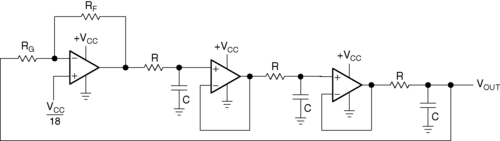
A.26. Bubba Oscillator
The bubba oscillator (Figure A.25) is another phase shift oscillator, but it takes advantage of the quad op amp package to yield some unique advantages. Each RC section is buffered by an op amp to prevent loading. When RG ≫ R, there is no loading in the circuit and the circuit yields theoretical performance.
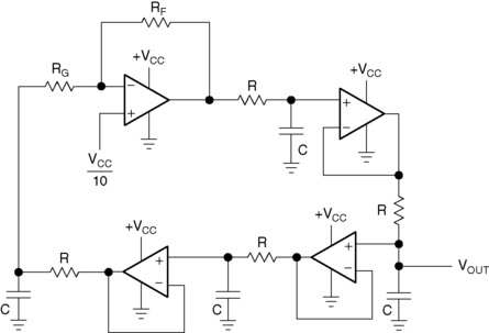 |
| Figure A.25 Bubba oscillator. |
Four RC sections require –45 ° phase shift per section to accumulate –180 ° phase shift. Each RC section contributes –45 ° phase shift when ω = 1/RC. The gain required for oscillation is G ≥ (1/0.707)4 = 4. Taking outputs from alternate sections yields low impedance quadrature outputs. When an output is taken from each op amp, the circuit delivers four 45 ° phase shifted sine waves.
The gain, A, must equal 4 for oscillation to occur. Very low distortion sine waves can be obtained from the junction of R and RG. When low distortion sine waves are required at all outputs, the gain should be distributed among the op amps. Gain distribution requires biasing of the other op amps, but it has no effect on the oscillator frequency. This oscillator has the best dφ/df of the phase shift oscillators, so it has minimum frequency drift. The reference voltage is set according to the equation VREF = VCC/2(1 + RF/RG) to center the output voltage at VCC/2. 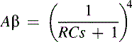
(A.26)
A.27. Triangle Oscillator
The triangle oscillator (Figure A.26) produces triangle waves and square waves. The op amp functions as an integrator. When the output voltage of the comparator is low, the output of the op amp charges C until the output voltage exceeds the hysteresis voltage set by R1 and RF and the reference voltage (VCC/2). At this point, the comparator output switches to a high state and the op amp integrates the voltage in a negative direction. The triangle wave (op amp output voltage swing) is given in Equation (A.27) and the frequency of oscillation is given in Equation (A.28): 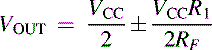
(A.27)
(A.28)
 |
| Figure A.26 Triangle oscillator. |
The op amp reference voltage can be adjusted to equalize the triangle rise and fall times.
A.28. Attenuation
An inverting attenuation circuit (this circuit is taken from the design notes of William Ezell) can be thought of as a T network in the RG resistor. It is shown in Figure A.27.
 |
| Figure A.27 Inverting attenuator circuit. |
RG is replaced by a T network consisting of RINA, RINB, and R3. A set of normalized values of the resistor R3 for various levels of attenuation is shown in Table A.1. For nontablated attenuation values, the resistance is 
(A.29)
To work with normalized values, do the following:
• Select a base value of resistance, usually between 1 kΩ and 100 kΩ for Rf and RIN.
• Divide RIN in two for RINA and RINB.
• Multiply the base value for Rf and RIN by 1 or 2, as shown in Figure A.27.
• Look up the normalization factor for R3 in Table A.1 and multiply it by the base value of resistance.
For example, if Rf is 20 kΩ, RINA and RINB are each 10 kΩ, and a 3 dB attenuator would use a 12.1 kΩ resistor.
A.29. Simulated Inductor
The circuit in Figure A.28 reverses the operation of a capacitor, making a simulated inductor. An inductor resists any change in its current, so when a DC voltage is applied to an inductance, the current rises slowly and the voltage falls as the external resistance becomes more significant.
 |
| Figure A.28 Simulated inductor. |
An inductor passes low frequencies more readily than high frequencies, the opposite of a capacitor. An ideal inductor has zero resistance. It passes DC without limitation, but it has infinite impedance at infinite frequency.
If a DC voltage is suddenly applied to the inverting input through resistor R1, the op amp ignores the sudden load because the change is also coupled directly to the noninverting input via C1. The op amp represents high impedance, just like an inductor.
As C1 charges through R2, the voltage across R2 falls, so the op amp draws current from the input through R1. This continues as the capacitor charges, and eventually the op amp has an input and output close to virtual ground (VCC/2).
When C1 is fully charged, resistor R1 limits the current flow; and this appears as a series resistance within the simulated inductor. This series resistance limits the Q of the inductor. Real inductors generally have much less resistance than the simulated variety.
A simulated inductor has some limitations:
• One end of the inductor is connected to virtual ground.
• The simulated inductor cannot be made with high Q, due to the series resistor R1.
• It does not have the same energy storage as a real inductor. The collapse of the magnetic field in a real inductor causes large voltage spikes of opposite polarity. The simulated inductor is limited to the voltage swing of the op amp, so the flyback pulse is limited to the voltage swing.
These factors limit the use of simulated inductors, but one application is perfect for simulated inductors: graphic equalizers.
To make a graphic equalizer, start with the basic op amp circuit shown in Figure A.29. The inductor L is shown with a parasitic resistance RS. It resonates with C2; and depending on the setting of potentiometer R2, the stage either produces a gain or a loss at the resonant frequency. The parasitic resistance of the inductor RS also sets the Q of the resonant circuit. Therefore, it determines the number of stages of equalization required to cover the audio band. In the right hand side of Figure A.29, the inductor L has been replaced by a simulated inductor circuit. To form the graphic equalizer, multiple stages of equalization are added in parallel by placing more potentiometers in parallel with R2.
 |
| Figure A.29 Graphic equalizer. |
A.30. Twin T Single Op Amp Bandpass and Notch Filters
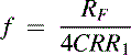
The filter design sections of this book presented some good topologies for bandpass and notch filters. However, some designers still believe superior performance can be achieved using the twin T topology. In the case of the notch filter, the only single op amp topology for a notch filter is the twin T configuration.
Twin T filters are based on a passive (RC) topology that uses three resistors and three capacitors. Matching these six passive components is critical; fortunately, it is also easy. The entire network can be constructed from a single value of resistance and a single value of capacitance, running them in parallel to create R3 and C3 in the twin T schematics shown in Figure A.30. Components from the same batch are likely to have very similar characteristics.
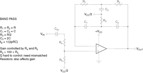 |
| Figure A.30 Single op amp bandpass filter. |
The bandpass circuit oscillates if the components are matched too closely. It is best to detune it slightly, by selecting the resistor to virtual ground to be one E-96 1% resistor value off, for instance.
The notch configuration of the twin T filter is shown in Figure A.31.
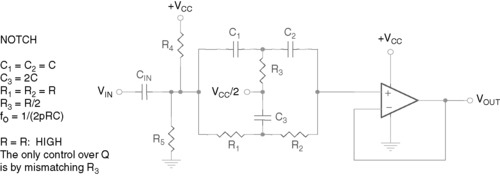 |
| Figure A.31 Single op amp notch filter. |
Figure A.32 shows a very nice way to lay out a twin T circuit. Considering all values of R and all values of C to be of equal value, for surface mount components, lay a pattern vertically with C, R, R, C on the top row and R, C, C, R on the bottom row. Input to the twin T connects to the C and R on the left, output from the C and R on the right connect all the top pads together, all of the bottom pads together, and connect the middle four components to VCC/2. The author has employed this strategy successfully in a high volume production product.
 |
| Figure A.32 Twin T network layout. |
A.31. Constant Current Generator
Figure A.33 shows a constant current generator. Equations (A.30) are a convenient current reference up to 20 mA:

(A.30)
 |
| Figure A.33 Constant current generator. |
A.32. Inverted Voltage Reference
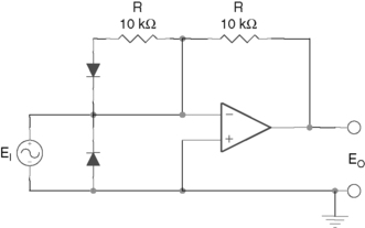
The circuit of Figure A.34 can be used to generate a negative voltage reference equal to a positive reference voltage. This circuit requires split supplies, however.
 |
| Figure A.34 Reference voltage supply. |
A.33. Power Booster
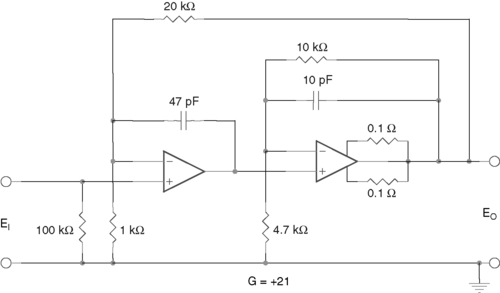
If a designer is careful, it is possible to create a composite amplifier whose important characteristics are better than either individual op amp.
The circuit in Figure A.35 shows a composite amplifier constructed from an OPA277 and an OPA512. The OPA512 is used as a power output buffer in the feedback loop of the OPA277. Its characteristics are tabulated in Table A.2.
 |
| Figure A.35 Composite op amp. |
The OPA512 has the highest slew rate and therefore is operated within a local closed loop. The slower OPA277 is operated within the outer loop. The 47 pF capacitor provides a small amount of phase shift to help stabilize the system. The resulting performance of the compound amplifier shows that the front end characteristics of the OPA277 are joined with the ±35 V at 10 A drive current capabilities out of the OPA512. The slew rate of the OPA277 is 0.8 V/μs. That slew rate is gained up times three in the OPA512 so that there is an effective slew rate for the compound amplifier of 2.4 V/μs.
A.34. Absolute Value
Figure A.36 shows an absolute value circuit, where +EI is the follower circuit, –EI is the inverter circuit, and EO = ∣EI∣. There is full wave rectification. Reverse the diodes to give EO = –∣EI∣.
 |
| Figure A.36 Absolute value circuit. |
A.35. Peak Follower
Figure A.37 shows a peak follower circuit with peak value memory. Use a low leakage capacitor. EO = EI maximum. Common mode input voltage must be observed.
 |
| Figure A.37 Peak follower circuit. |
A.36. Precision Rectifier
Figure A.38 shows a precision rectifier circuit.
(A.31)
 |
| Figure A.38 Precision rectifier. |
Placing rectifiers in feedback loop decreases nonlinearity to a very small value.
A.37. AC to DC Converter
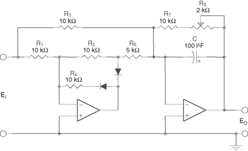 |
| Figure A.39 AC to DC converter. |
This is used for precision conversion for measurement or control. It features full wave rectifier with a smoothing filter.
A.38. Full Wave Rectifier
Figure A.40 shows a full wave rectifier. This is a precision absolute value circuit.
 |
| Figure A.40 Full wave rectifier. |
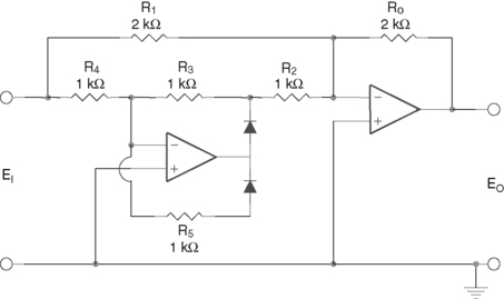
A.39. Tone Control
One rather unusual op amp circuit is the tone control circuit (Figure A.41). It bears some superficial resemblance to the twin T circuit configuration, but it does not have a twin T topology. It is actually a hybrid of one pole low pass and high pass circuits with gain and attenuation.
 |
| Figure A.41 Tone control. |
The midrange for the tone adjustments is 1 kHz. It gives about ±20 dB of boost and cut for bass and treble. The circuit is a minimum component solution, seeking to limit cost. This circuit, unlike similar circuits, uses linear potentiometers instead of logarithmic. Two different potentiometer values are unavoidable, but the capacitors are the same value except for the coupling capacitor. The ideal value of capacitor is 0.016 μF, which is an E-24 value, so the more common E-12 value of 0.015 μF is used instead. Even that value is a bit odd, but it is easier to find an oddball capacitor value than it is an oddball potentiometer value.
The plots in Figure A.42 show the response of the circuit with the potentiometers at the extremes and at one quarter and three quarter positions. The mid position, although not shown, is flat to within a few millidecibels. The compromises involved in reducing the circuit cost and using linear potentiometers lead to some slight nonlinearities. The one quarter and three quarter positions are not exactly 10 and –10dB, meaning that the potentiometers are most sensitive toward the end of their travel. This may be preferable to the listener, giving a fine adjustment near the middle of the potentiometers and more rapid adjustment near the extreme positions. The center frequency shifts slightly, but this should be inaudible. The frequencies nearer the midrange are adjusted more rapidly than the frequency extremes, which also may be more desirable to the listener. A tone control is not a precision audio circuit, and therefore the listener may prefer these compromises.
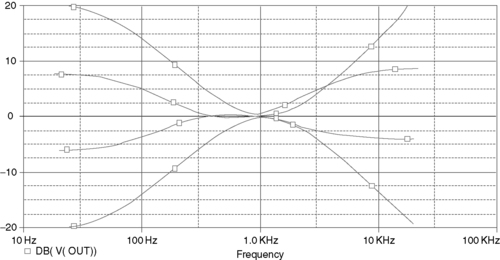 |
| Figure A.42 Tone control response. |
A.40. Curve Fitting Filters
Analog designers are often asked to design low pass and high pass filter stages for maximum rejection of frequencies that are out of band. This is not always the case, however. Sometimes the designer is asked to design a circuit that conforms to a specified frequency response curve. This can be a challenging task, particularly if all the designer knows is that a single pole filter rolls off 20 dB per decade and double pole 40 dB per decade. How does the designer implement a different roll-off?
To begin with, it is not possible to get more out of a filter than it is designed to produce. A single pole will give no more than 20 dB per decade—and cannot be increased or decreased. More roll-off demands a double pole filter with 40 dB per decade. Obtaining different roll-off characteristics is done by allowing filters at closely spaced frequencies to overlap.
One popular curve fitting application is the RIAA equalization (Figure A.43), which compensates for equalization applied to vinyl record albums during manufacture. Many newer pieces of audio gear have omitted the RIAA equalization circuit completely, assuming that the majority of users do not desire the function. In spite of the enormous popularity of audio CDs, there is still a dedicated group of audiophiles that have a large library of record albums, titles that are not available on CD or are out of print.
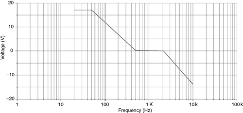 |
| Figure A.43 RIAA equalization curve. |
RIAA has three break points:
• 17 dB from 20 to 50 Hz.
• 0 dB from 500 to 2120 Hz.
• –13.7 dB at 10 kHz.
RIAA equalization curves often include another break point at 10 Hz to limit low frequency “rumble” effects that could resonate with the turntable's tonearm. The standard input impedance in the circuits shown here is 47 kΩ. This impedance makes a convenient place to inject DC offset into single supply circuits, so it is isolated from the phono cartridge by an input capacitance. The phono cartridge output is assumed to be 12 mV.
Application circuits were evaluated from many sources in print and on the Web. Many of these either did not work at all, did not easily translate to single supply operation, or deviated markedly from the RIAA specification. Many circuits have been proposed for this function; in fact, competitions have been held to propose the best. To this fray, this volume respectfully submits Figure A.44.
 |
| Figure A.44 RIAA equalization preamplifier. |
This circuit topology is very flexible—most of the RIAA break points are independently adjustable:
• R1 and C1 set the low frequency response.
• U1A, R2, and R3 control the overall gain of the circuit.
• R4 and R5 control the low frequency gain.
• R5 and C2 control the 50 Hz low frequency break point.
• C3, C4, C5, R6, R7, and U1C form a 500 Hz high pass filter that reverses the effect of the 50 Hz low pass filter and flattens the response through 1 kHz until the 2120 Hz low pass filter begins to affect the response.
• R8, R9, R10, C6, C7, U1D form the 2120 Hz low pass filter, the input resistor has been split into a summing resistor.
The overall response of the filter is shown in Figure A.45.
 |
| Figure A.45 RIAA response. |
The 500 Hz response is above the ideal curve by 0.8 dB, and the 2120 Hz response is below the ideal curve by –1.3 dB. This circuit is about the best that can be done without many more op amps and complex design techniques. It should produce very aesthetically pleasing sound reproduction.
Further Reading
1. Thomas R. Brown, Handbook of Operational Amplifier Applications. (1963) Texas Instruments; Application Report SBOA092A.
2. Bruce Carter, An Audio Circuit Collection. (2000) Texas Instruments, Dallas; parts 1–3.
..................Content has been hidden....................
You can't read the all page of ebook, please click here login for view all page.