7
Ferroelectric Properties
Tobias Leonhard, Holger Röhm, Alexander D. Schulz and Alexander Colsmann
Karlsruhe Institute of Technology (KIT), Material Research Center for Energy Systems (MZE), Strasse am Forum 7, 76131 Karlsruhe, Germany
7.1 On the Importance of Ferroelectricity in Hybrid Perovskite Solar Cells
Among the distinct properties of light‐harvesting organic metal halide (OMH) perovskites are their low charge carrier recombination at traps states (Shockley–Read–Hall [SRH] recombination) [1] and their excellent charge carrier transport [2–4]. Recent theoretic and experimental findings have pointed out that some OMH perovskites are ferroelectric and that the corresponding microscopic internal fields may partly be the origin of the low charge carrier recombination and hence the excellent device performance [5–9]. Not only does a ferroelectric light‐harvesting layer produce solar cells with different charge carrier dynamics. The inherent switchability of ferroelectric materials between at least two states under electrical fields also strongly affects solar cell operation, characterization, and stability [10, 11].
This chapter reviews the characterization techniques toward the investigation of ferroelectricity in (light‐harvesting) semiconductors, including common pitfalls, and summarizes different data interpretations. Not least, important implications of ferroelectric light‐harvesting semiconductors will be discussed with respect to solar cell performance and characterization.
In the literature, the term “ferroelectric solar cells” has been used in conjunction with solar cells that utilize the bulk‐photovoltaic effect: [12] microscopic electric fields in insulating ferroelectric domain assemblies produce higher‐than‐usual photovoltages (similar to tandem solar cells), but their negligible device currents, to date, render the concept rather inefficient. In contrast, this chapter deliberately focuses on semiconducting thin films, which operate as single light‐harvesting layers in solar cells.
7.2 Ferroelectricity
The (macroscopic) textbook definition of ferroelectricity is the existence of a spontaneous polarization that is switchable between at least two polarization states under an external electric field [13]. Microscopically, ferroelectric materials form domains with spontaneous polarization. These properties of ferroelectric materials find their origin in the crystal structure.
7.2.1 Crystallographic Considerations
The crystal structure and its symmetry determine most of the fundamental properties of a crystalline material such as its conductivity, its band structure, and its ferroic properties, the latter of which includes ferromagneticity, ferroelasticity, and ferroelectricity. Symmetry elements, including rotational symmetries, mirror symmetries, and inversion, define 32 fundamental crystal classes. In general, ferroelectricity requires a unit cell that exhibits a polar axis, which can only occur in non‐centrosymmetric crystals. Non‐centrosymmetry is synonymous with a lack of inversion symmetry in the unit cell of the crystal. Figure 7.1a illustrates non‐centrosymmetry in a hypothetic two‐dimensional crystal comprising two different atomic constituents. The polar axes prevent the congruent lattice inversion at the center of the unit cell [14].

Figure 7.1 Illustration of the piezoelectric effect in a hypothetic two‐dimensional, non‐centrosymmetric crystal comprising two types of atoms. (a) The configuration of atoms forms three polar axes, which preclude inversion symmetry. (b) Upon application of a mechanical force along one of the polar axes, the displacement of atoms creates a polarization.
Out of the 32 crystal classes, 20 exhibit one or more polar axes in the unit cell, making the crystal piezoelectric. By applying an external mechanical force along one of the polar axes as illustrated in Figure 7.1b, atoms are displaced, inducing an electric polarization and hence a charging of the crystal faces perpendicular to the polar axis. Similarly, an externally applied electrical field deforms the crystal along one of the polar axes (inverse or converse piezoelectric effect). In 10 out of the 20 piezoelectric crystal classes, a unique polar axis exists and intrinsic dipole moments in the unit cell form a spontaneous polarization even in the absence of an external electric field [15]. In these crystal classes the polarization magnitude changes upon application of a temperature gradient, and hence the crystal is considered pyroelectric. Changes in the permanent dipole moments become detectable in variations of the surface potential until surface charges have screened and compensated the pyroelectric polarization. Among the pyroelectric materials, some crystals exhibit a permanent spontaneous polarization ![]() with at least two different equilibrium states. The crystal can switch between those states if a sufficiently large external electric field is applied. The occurrence of different equilibrium states of spontaneous polarization
with at least two different equilibrium states. The crystal can switch between those states if a sufficiently large external electric field is applied. The occurrence of different equilibrium states of spontaneous polarization ![]() characterizes ferroelectricity. Thus, every ferroelectric material is also pyroelectric and piezoelectric, but not necessarily vice versa. The spontaneous polarization in ferroelectrics can originate either from ordered intrinsic electric dipole moments or from displaced atoms in the unit cells, thus creating a polar axis [14]. For example, in a tetragonal crystal (axes cT > aT = bT; angles between axes: 90°), displaced atoms along the cT‐axis can induce ferroelectricity. Above the Curie temperature TC, which is a material‐specific property, the crystal transitions to a non‐ferroelectric (paraelectric) state with high symmetry. In the example of a tetragonal crystal, a transition from the tetragonal structure to a cubic structure is observed when exceeding TC. Similarly, upon cooling below TC, the symmetry is reduced and modifications in the crystal structure and deformations of the unit cells induce mechanical strain in the crystal lattice and generate a polar axis. Strain produces a uniform parallel orientation of electric dipoles within a group of ferroelectric unit cells, which adds up to strong polarization fields in the crystal (in contrast to antiferroelectrics where the antiparallel polarization of neighboring unit cells diminishes the macroscopic effect of polarization). To compensate the electric fields from the internal polarization
characterizes ferroelectricity. Thus, every ferroelectric material is also pyroelectric and piezoelectric, but not necessarily vice versa. The spontaneous polarization in ferroelectrics can originate either from ordered intrinsic electric dipole moments or from displaced atoms in the unit cells, thus creating a polar axis [14]. For example, in a tetragonal crystal (axes cT > aT = bT; angles between axes: 90°), displaced atoms along the cT‐axis can induce ferroelectricity. Above the Curie temperature TC, which is a material‐specific property, the crystal transitions to a non‐ferroelectric (paraelectric) state with high symmetry. In the example of a tetragonal crystal, a transition from the tetragonal structure to a cubic structure is observed when exceeding TC. Similarly, upon cooling below TC, the symmetry is reduced and modifications in the crystal structure and deformations of the unit cells induce mechanical strain in the crystal lattice and generate a polar axis. Strain produces a uniform parallel orientation of electric dipoles within a group of ferroelectric unit cells, which adds up to strong polarization fields in the crystal (in contrast to antiferroelectrics where the antiparallel polarization of neighboring unit cells diminishes the macroscopic effect of polarization). To compensate the electric fields from the internal polarization![]() , screening charges accumulate at the crystal surface and form depolarization fields
, screening charges accumulate at the crystal surface and form depolarization fields![]() [15]. The presence of at least two distinct polarization states with different orientation fosters the subdivision of ferroelectric materials into energetically more favorable domains. Such domains represent groups of unit cells with uniformly oriented polar axes. The formation of domains minimizes the energy of the system as an interplay of mechanical stress, internal polarization, and screening charges. Domain walls separate domains. Figure 7.2 illustrates different domain configurations for a cubic to tetragonal phase transition. 180°‐domains with antiparallel polarization orientation between neighboring domains compensate strong depolarization fields
[15]. The presence of at least two distinct polarization states with different orientation fosters the subdivision of ferroelectric materials into energetically more favorable domains. Such domains represent groups of unit cells with uniformly oriented polar axes. The formation of domains minimizes the energy of the system as an interplay of mechanical stress, internal polarization, and screening charges. Domain walls separate domains. Figure 7.2 illustrates different domain configurations for a cubic to tetragonal phase transition. 180°‐domains with antiparallel polarization orientation between neighboring domains compensate strong depolarization fields![]() . Mechanical stress originating from the phase transition or external pressure can render other domain configurations energetically more favorable. 90°‐domains, where the polar axes between neighboring domains form an angle of 90°, reduce both mechanical strain and polarization fields. Hence, the observation of 90°‐domains often indicates that both mechanical strain and polarization coexist and drive the crystal formation [16, 17]. Details of the interaction of mechanical strain and polarization as well as further background on the mechanisms behind domain formation and domain characteristics are discussed in the literature [18, 19].
. Mechanical stress originating from the phase transition or external pressure can render other domain configurations energetically more favorable. 90°‐domains, where the polar axes between neighboring domains form an angle of 90°, reduce both mechanical strain and polarization fields. Hence, the observation of 90°‐domains often indicates that both mechanical strain and polarization coexist and drive the crystal formation [16, 17]. Details of the interaction of mechanical strain and polarization as well as further background on the mechanisms behind domain formation and domain characteristics are discussed in the literature [18, 19].
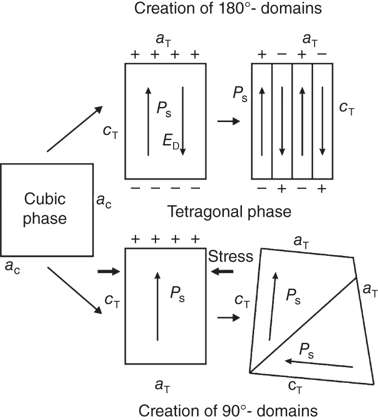
Figure 7.2 Illustration of principal ferroelectric domain formation in a tetragonal crystal. Upon cooling below the Curie temperature TC, a non‐ferroelectric cubic crystal transitions to a tetragonal ferroelectric phase by deformation, whereby two types of ferroelectric domain configurations can form. Top: In order to compensate spontaneous polarization and induced surface charges, alternating domains with antiparallel polarization orientation form, creating 180°‐domains. Bottom: Mediated by mechanical stress, the crystal forms 90°‐domains, partially compensating stress and polarization.
Source: Damjanovic [15]. Reprinted (adapted) with permission from Damjanovic 1998, DOI: 10.1088/0034‐4885/61/9/002. © IOP Publishing. Reproduced with permission. All rights reserved.
Upon phase transition at TC, crystals can also form states of spontaneous mechanical strain as a mechanical equivalent to ferroelectricity [20]. This ferroelasticity requires the existence of two strain states in the material, which are switchable under sufficiently strong external mechanical stresses [21, 22]. These strain states are equivalent in crystal structure [23] and are induced by small displacements of atoms in the crystal [24]. Internal strain often coexists with spontaneous polarization: common ferroelectric materials exhibit ferroelastic properties, while ferroelasticity can occur without ferroelectricity. Telling apart ferroelastic and ferroelectric crystals only by measurements of their piezoelectric properties can bear some pitfalls as discussed further. Commonly, ferroelectric and purely ferroelastic (non‐ferroelectric) materials can be distinguished by poling experiments, since only the internal polarization ![]() of a ferroelectric material responds to an external electric field. Hence, poling events in which the polarization switches between its equilibrium states following the external electric field are considered a classical hallmark of ferroelectricity [13].
of a ferroelectric material responds to an external electric field. Hence, poling events in which the polarization switches between its equilibrium states following the external electric field are considered a classical hallmark of ferroelectricity [13].
In ferroelectric insulators, poling is investigated by measurements of the characteristic polarization hysteresis as a function of the electric field as illustrated in Figure 7.3. Microscopically, the hysteresis corresponds to a reorganization of the ferroelectric domains with distinct polarization orientations, which are represented by arrows in Figure 7.3. In the unpoled state (A), domains organize to minimize the formation energy by minimization of the net polarization, strain, and screening charges. Upon application of an increasing external electric field, the polar dipoles gradually align, and the domains change their shape and position, until most of the domains exhibit uniform orientation. Macroscopically, the latter shows as a saturation of the polarization magnitude ![]() for further increasing electric fields (B). During this process of unit cell ordering, the strain in the crystal can increase, enabled by the energy provided by the electric field. Upon a subsequent gradual release of the electric field, the domains return to their original state to minimize strain. However, some preferential polarization orientation persists as remanent polarization
for further increasing electric fields (B). During this process of unit cell ordering, the strain in the crystal can increase, enabled by the energy provided by the electric field. Upon a subsequent gradual release of the electric field, the domains return to their original state to minimize strain. However, some preferential polarization orientation persists as remanent polarization ![]() , even if the external electric field is reduced to zero (C). In order for zero internal net polarization (P = 0), additional energy is required from a coercive field EC in reverse direction (D). By increasing the reverse electric field, the same process of polarization and domain pattern alignment occurs (E), but in reverse direction, followed by a negative remanent polarization (F) under a decreasing reverse electric field, altogether generating a point‐symmetric hysteresis curve. The shape of the hysteresis depends not only on the strength of spontaneous polarization, but also on sample features such as the geometry, crystal defects, mechanical stress, and temperature [15]. Although the investigation of the polarizability of the sample by hysteresis measurements is well established to prove or disprove ferroelectricity, its application to certain sample geometries such as thin films, as commonly used in modern solar cells, can become challenging. Local thickness variations can induce strongly enhanced electric fields, producing local thermal damage before any switching of polarization is accomplished. Switching becomes even more challenging if the material under investigation is a semiconductor that exhibits conductivity of photo‐generated charge carriers and mobile ions, both of which can be found in modern OMH perovskites.
, even if the external electric field is reduced to zero (C). In order for zero internal net polarization (P = 0), additional energy is required from a coercive field EC in reverse direction (D). By increasing the reverse electric field, the same process of polarization and domain pattern alignment occurs (E), but in reverse direction, followed by a negative remanent polarization (F) under a decreasing reverse electric field, altogether generating a point‐symmetric hysteresis curve. The shape of the hysteresis depends not only on the strength of spontaneous polarization, but also on sample features such as the geometry, crystal defects, mechanical stress, and temperature [15]. Although the investigation of the polarizability of the sample by hysteresis measurements is well established to prove or disprove ferroelectricity, its application to certain sample geometries such as thin films, as commonly used in modern solar cells, can become challenging. Local thickness variations can induce strongly enhanced electric fields, producing local thermal damage before any switching of polarization is accomplished. Switching becomes even more challenging if the material under investigation is a semiconductor that exhibits conductivity of photo‐generated charge carriers and mobile ions, both of which can be found in modern OMH perovskites.

Figure 7.3 Electric poling in a ferroelectric crystal. The switching of the spontaneous polarization can be observed macroscopically in typical hysteresis curves and in modifications of domain patterns on the microscale. The macroscopic effect is connected to characteristic states of the crystal describing distinct polarization orientations, labeled A–G. The polarization aligns toward the external applied electric field, changing domain sizes and moving domain walls.
7.2.2 Ferroelectricity in Thin Films
Thin films are characterized by high aspect ratios with large lateral dimensions (x‐ and y‐direction) and a small vertical dimension (z‐direction, film thickness). This geometry reduces the symmetry of the system and leads to anisotropic stress upon changes in temperature and in particular upon phase transition, driving the formation of domains and their width within crystalline thin films [16, 25].
Thin film properties are strongly affected by the interfaces toward neighboring layers, substrate surfaces, or surrounding atmosphere. Each interface can be considered a defect of the crystal and, therefore, influences the thin film properties [26]. The binding forces between a crystalline thin film and neighboring solid materials lead to clamping, i.e. a transfer of stress and restriction of lattice expansion. Additional defects at the thin film surface, at interfaces, or in the bulk can modulate the microstructure of the crystal and thereby influence domain formation as well as shape and position of domain walls (pinning) [27].
7.2.3 Crystallography of MAPbI3 Thin Films
A fundamental requirement for the presence of a spontaneous (ferroelectric) polarization is the lack of centrosymmetry [18]. At room temperature, MAPbI3 has a tetragonal crystal structure. At TC = 327 K and beyond, a transition occurs from the tetragonal to the cubic phase [28]. Notably, both phases can appear in the temperature regime in which solar cells usually operate [29]. The centrosymmetric cubic phase above TC is described consistently [28, 30], and the literature also widely agrees on a tetragonal crystal structure at room temperature (below TC) [28, 31]. However, while most reports conclude on a non‐centrosymmetric nature of MAPbI3 [32–34], some describe a centrosymmetric crystal structure [35].
In general, most ferroelectrics with perovskite structure exhibit high intrinsic dielectric constants, reflecting their intrinsic polarization [36]. The intrinsic polarization typically originates from the distortion of the BX6 octahedron, i.e. displacements of the B‐site cations vs. the X‐site anions [37, 38]. In common ferroelectrics such as barium titanate (BaTiO3) or lead zirconate‐titanate (Pb(Zr,Ti)O3, PZT), the displacement can be rather strong resulting in a significant polarization [39, 40]. In contrast, MAPbI3 possesses only a small tetragonality with a c/a ratio close to unity (c/a = 1.009) [34]. In addition, neighboring PbI6 octahedra are alternatingly tilted [33, 41], and additional distortion of the crystal lattice from the organic molecule occurs [42]. Simulations have shown that the polar moment in tetragonal MAPbI3 is expected to be rather small [9], limiting its experimental accessibility. Breternitz et al. recently pointed out that the formation of twin domains may be one of the reasons for the contradicting reports [34]. This twinning may lead to seemingly high symmetry on a macroscopic scale, impeding a correct classification to symmetry elements [34]. They proposed a microscopic symmetry breaking in the MAPbI3 unit cell due to the distinct shift of iodine atoms caused by the interaction with the organic molecule methylammonium (MA), which would only be visible to specific measurement techniques. Others reported that the orientation of MA, which comprises an intrinsic dipole moment, might contribute to a polarization of the unit cell [6, 42, 43].
7.3 Probing Ferroelectricity on the Microscale
The presumably small polarization coupled with other special features of hybrid perovskites, such as the intrinsic conductivity for both charge carriers and mobile ions, calls for advanced measurement techniques to probe ferroelectricity and effects thereof on the microscale. Techniques based on atomic force microscopy (AFM) offer a number of versatile opportunities to probe the genuine features of ferroelectricity while mostly avoiding sample damage or changes to the sample properties during the measurement process. In particular, piezoresponse force microscopy (PFM) is one of the most relevant characterization tools for the investigation of ferroelectricity.
7.3.1 Atomic Force Microscopy
Generally, AFM enables the nondestructive investigation of the sample topography from the nanometer to the micrometer regime by measuring the interacting forces between the tip and the sample [44, 45]. For this purpose, the tip is mounted onto a cantilever, which possesses a certain spring constant and a specific resonance frequency. When the tip approaches the sample surface, the sample produces a force onto the tip and the cantilever deforms. This deflection is monitored with a laser beam that is reflected from the cantilever onto a four‐quadrant diode as illustrated in Figure 7.4. In contact mode, the tip scans the sample surface in permanent contact. The left side of the schematic in Figure 7.4 summarizes the processing of the information on the tip movement. In a nutshell, the displacement of the laser beam, which is monitored on the photodiode, is processed by a feedback system. This feedback system then adjusts the tip height through the tip–sample distance control to hold the interacting forces and hence a specific cantilever deflection constant [46]. The feedback information yields a topographic map for each position of the sample surface.
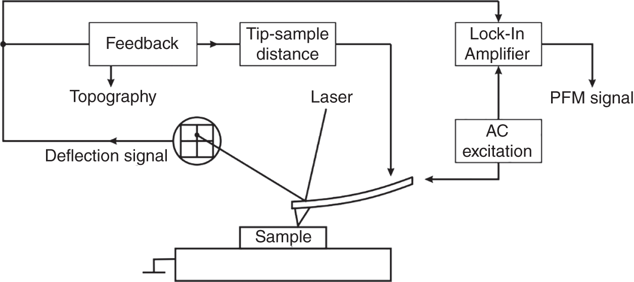
Figure 7.4 Schematic of the implementation of an AFM measurement setup with additional components for PFM. The cantilever deflection is tracked with a laser, which is monitored on a four‐quadrant photodetector. Left: The control unit receives the laser signal from the photodetector, which reproduces the interaction of tip and sample, and adjusts the height of the tip for constant force onto the sample in contact mode. The topography signal is then obtained from tracing the tip adjustment. Right: To conduct PFM, an additional AC bias is applied and the piezoelectric response of the sample is measured through the tip deflection. To disentangle piezoresponse and topography, lock‐in amplifiers are used.
7.3.2 Piezoresponse Force Microscopy
Being part of the AFM family, PFM is a powerful characterization tool to explore the piezoelectric response of samples with high spatial resolution [47, 48]. In particular, it allows the characterization of ferroelectric domains with distinct polarization by their different piezoresponse on the nanometer scale [49]. In contrast to other microscopy techniques, PFM does not require any labor‐intensive sample preparation such as polishing and etching [50]. PFM utilizes the inverse piezoelectric effect by application of an external AC‐bias VAC between the conductive AFM tip and the sample and by simultaneous measurement of the changes of the sample dimensions. As visualized in Figure 7.5, the time‐dependent excitation bias VAC(t) = V0 · sin ωt and hence the electric field ![]() follow a sine function. The ideal undelayed response of the sample to this bias shows periodic expansions and contractions following the piezoelectric strain [51].
follow a sine function. The ideal undelayed response of the sample to this bias shows periodic expansions and contractions following the piezoelectric strain [51].
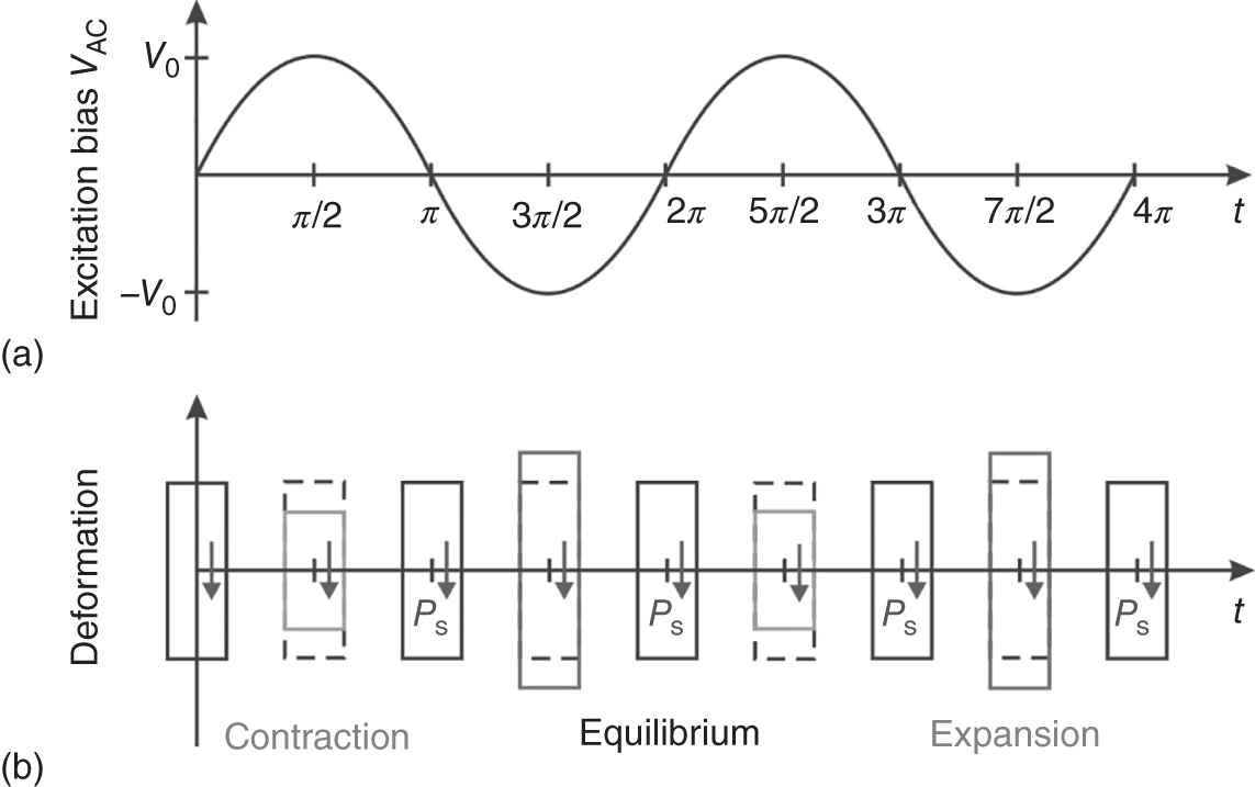
Figure 7.5 The measurement principle of PFM utilizes the response of the sample to the time‐dependent AC‐bias VAC (inverse piezoelectric effect). (a + b) The sinusoidal VAC causes periodic expansions and contractions of an individual domain with the spontaneous polarization  pointing downward. Antiparallel
  and
and  incur sample contraction, while parallel
  and
and  cause sample expansion relative to the equilibrium state, where no electric field is applied.
Figure 7.5b depicts the corresponding time‐dependent deformation of an individual ferroelectric domain with its polarization ![]() pointing downward. While the sample is in equilibrium at VAC = 0 (for ωt = 0, π, 2π, …), the sample expands if
pointing downward. While the sample is in equilibrium at VAC = 0 (for ωt = 0, π, 2π, …), the sample expands if ![]() is parallel to
is parallel to ![]() and contracts if
and contracts if ![]() is antiparallel to
is antiparallel to ![]() . In PFM, the tip acts as both stimulator and detector. The expansions and contractions of the sample under the electric bias become detectable by deflections of the cantilever, which are generally monitored by the reflected laser on the photodiode, and hence superimpose the topography signal [52]. Thus, PFM is susceptible to topographic cross talk, which is why smooth sample surfaces help toward the interpretation of data.
. In PFM, the tip acts as both stimulator and detector. The expansions and contractions of the sample under the electric bias become detectable by deflections of the cantilever, which are generally monitored by the reflected laser on the photodiode, and hence superimpose the topography signal [52]. Thus, PFM is susceptible to topographic cross talk, which is why smooth sample surfaces help toward the interpretation of data.
Figure 7.6 depicts four principal orientations of spontaneous sample polarization and illustrates the respective displacement of the AFM tip by the piezomechanical strain induced by the applied electric field ![]() . Figure 7.6a,b illustrate the expansion or contraction of the sample and the corresponding up‐ and down‐deflection of tip and laser, if the polarization (or components thereof) is oriented parallel or antiparallel to the vertical external electric field. If thepolarization (or components thereof) is oriented perpendicular to the vertical external electric field, as depicted in Figure 7.6c,d, shearing of the material becomes visible in a torsion of the cantilever, which is tracked by a left and a right deflection of the laser. Hence, deflection and torsion of the cantilever allow the differentiation of vertical and horizontal piezoresponses of the sample and thus the differentiation of vertical and horizontal ferroelectric polarization components, commonly referred to as vertical piezoresponse force microscopy (VPFM) and lateral piezoresponse force microscopy (LPFM). In order to obtain PFM data and to disentangle the deflection of the cantilever caused by the piezoelectric effect and the topography, lock‐in amplifiers are used (Figure 7.4, right side) [51]. The additional lock‐in amplifiers transform the piezoelectric signal from a deflection into an output voltage with amplitude A and phase ϕ [50]. Ideally, the PFM amplitude represents the magnitude of the internal polarization of the sample, whereas the phase shows the orientation of the polarization. This behavior is illustrated in Figure 7.7a on an exemplary ideal ferroelectric sample with vertical domains of alternating (up‐ and downward) polarization. Upon scanning across domain assemblies with an AFM tip, VPFM produces a constant PFM amplitude A (Figure 7.7b), only decreasing at domain walls. The corresponding PFM phase in Figure 7.7c depends on the orientation of
. Figure 7.6a,b illustrate the expansion or contraction of the sample and the corresponding up‐ and down‐deflection of tip and laser, if the polarization (or components thereof) is oriented parallel or antiparallel to the vertical external electric field. If thepolarization (or components thereof) is oriented perpendicular to the vertical external electric field, as depicted in Figure 7.6c,d, shearing of the material becomes visible in a torsion of the cantilever, which is tracked by a left and a right deflection of the laser. Hence, deflection and torsion of the cantilever allow the differentiation of vertical and horizontal piezoresponses of the sample and thus the differentiation of vertical and horizontal ferroelectric polarization components, commonly referred to as vertical piezoresponse force microscopy (VPFM) and lateral piezoresponse force microscopy (LPFM). In order to obtain PFM data and to disentangle the deflection of the cantilever caused by the piezoelectric effect and the topography, lock‐in amplifiers are used (Figure 7.4, right side) [51]. The additional lock‐in amplifiers transform the piezoelectric signal from a deflection into an output voltage with amplitude A and phase ϕ [50]. Ideally, the PFM amplitude represents the magnitude of the internal polarization of the sample, whereas the phase shows the orientation of the polarization. This behavior is illustrated in Figure 7.7a on an exemplary ideal ferroelectric sample with vertical domains of alternating (up‐ and downward) polarization. Upon scanning across domain assemblies with an AFM tip, VPFM produces a constant PFM amplitude A (Figure 7.7b), only decreasing at domain walls. The corresponding PFM phase in Figure 7.7c depends on the orientation of ![]() relative to the electric excitation field and yields a phase contrast of 180° between neighboring domains. Hence, a PFM micrograph represents a map of the piezomechanical sample response and assigns a distinct PFM amplitude and phase to each pixel. The lateral resolution of the PFM image is in the nanometer regime [49, 53] and depends on the tip radius r, which is usually in the range of r = 20–30 nm, [50]; however, it is also affected by the (local) elastic, dielectric, and topographic properties of the sample [51, 54].
relative to the electric excitation field and yields a phase contrast of 180° between neighboring domains. Hence, a PFM micrograph represents a map of the piezomechanical sample response and assigns a distinct PFM amplitude and phase to each pixel. The lateral resolution of the PFM image is in the nanometer regime [49, 53] and depends on the tip radius r, which is usually in the range of r = 20–30 nm, [50]; however, it is also affected by the (local) elastic, dielectric, and topographic properties of the sample [51, 54].

Figure 7.6 Probing the piezoelectric sample response. Depending on the relative orientation of the electric excitation field  and the sample polarization
  , the sample expands or contracts, inducing tip deflections monitored by a laser beam on a photodiode. (a + b) If
  is oriented out‐of‐plane and (anti‐)parallel to
  , a vertical piezoresponse force microscopy (VPFM) signal is produced. (c + d) In case of in‐plane polarization with an orientation perpendicular to
  , shearing of the sample causes a torsion of the cantilever and produces a lateral piezoresponse force microscopy (LPFM) signal.

Figure 7.7 (a) Illustration of PFM measurements on a sample with alternating polarization orientation, exemplified on 180° vertical polarization (alternating up‐ and downward polarization). (b) Applying PFM on the sample, the domains produce a constantly high PFM amplitude, which represents the strength of spontaneous polarization. At domain boundaries where the polarization changes, the amplitude decreases. (c) The corresponding PFM phase allows conclusions on the relative orientation of the spontaneous polarization, here showing a 180° contrast between domains of different polarization.
Sometimes, weak piezoelectric responses may conceal the true nature of the sample under investigation. A weak signal may originate from weak spontaneous polarization in the crystal or from a thin layer comprising only a small number of unit cells in z‐direction that contribute to the signal in a thin film. In particular, the conductivity of the sample can limit the applicable AC bias magnitude Vmax and hence the PFM contrast. Increasing the AC bias beyond Vmax can induce reorientations of ![]() , i.e. ferroelectric poling, or damage the sample by electric currents [55]. To avert weak PFM signals and to enhance the signal‐to‐noise ratio, samples are often measured near contact resonance of the tip–sample system (Figure 7.8) [57]. The mechanically oscillating system of tip and sample in contact resonates to a certain frequency f1 of the excitation bias (Figure 7.8a,b). If the AC frequency is constant during a PFM scan, this PFM technique is referred to as resonance‐enhanced single‐frequency piezoresponse force microscopy (sf‐PFM). On the downside, sf‐PFM is very susceptible to topographic cross talk, because variations of the topography can change the tip–sample system and its resonance frequency, possibly producing variations in the PFM amplification. Consequently, resonance‐enhanced sf‐PFM can impede both the quantitative analysis of the PFM amplitude and the assignment of polarization orientations in ferroelectric domains. This is why the measurement parameters must be selected carefully to allow the interpretation of resonance‐enhanced sf‐PFM data for ferroelectric features, and potential features from topographic cross talk must be considered during PFM data interpretation.
, i.e. ferroelectric poling, or damage the sample by electric currents [55]. To avert weak PFM signals and to enhance the signal‐to‐noise ratio, samples are often measured near contact resonance of the tip–sample system (Figure 7.8) [57]. The mechanically oscillating system of tip and sample in contact resonates to a certain frequency f1 of the excitation bias (Figure 7.8a,b). If the AC frequency is constant during a PFM scan, this PFM technique is referred to as resonance‐enhanced single‐frequency piezoresponse force microscopy (sf‐PFM). On the downside, sf‐PFM is very susceptible to topographic cross talk, because variations of the topography can change the tip–sample system and its resonance frequency, possibly producing variations in the PFM amplification. Consequently, resonance‐enhanced sf‐PFM can impede both the quantitative analysis of the PFM amplitude and the assignment of polarization orientations in ferroelectric domains. This is why the measurement parameters must be selected carefully to allow the interpretation of resonance‐enhanced sf‐PFM data for ferroelectric features, and potential features from topographic cross talk must be considered during PFM data interpretation.

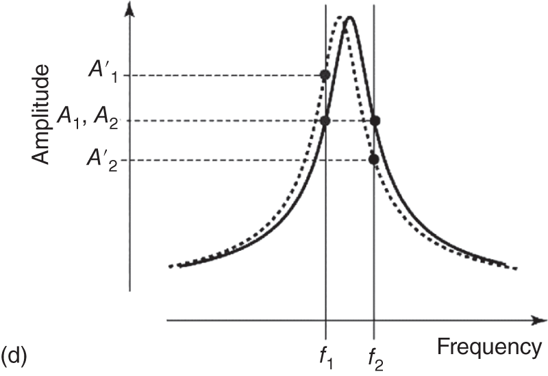
Figure 7.8 Schematic implementation of single‐frequency enhanced piezoresponse force microscopy (sf‐PFM) and Dual AC resonance tracking piezoresponse force microscopy (DART‐PFM). (a, b) In sf‐PFM, the frequency f1 of the AC excitation bias is set close to the contact resonance of the tip–sample system, such that the PFM signal is amplified and the signal‐to‐noise ratio is enhanced. Yet, topography features may change the resonance conditions, producing artifacts.
Source: Ch. 1.
Reprinted (adapted) with permission from Oxford Instruments GmbH Asylum Research, Asylum User Guide, Chapter Rev. 621. Copyright (2010) Oxford Instruments GmbH Asylum Research. (c, d) In DART‐PFM, the cantilever is excited at the sum of two frequencies f1 and f2, which are set below and above the contact resonance. Using a second lock‐in amplifier allows tracking of the resonance, warranting a constant amplification and a decoupling of the PFM signal and the topographic cross talk.
Source: Rodriguez et al. [56]. Reprinted (adapted) with permission from Rodriguez et al. 2007, DOI: 10.1088/0957‐4484/18/47/475504. © IOP Publishing. Reproduced with permission. All rights reserved.
Dual AC resonance tracking piezoresponse force microscopy (DART‐PFM) is an advanced PFM mode that enables a consistent resonance amplification with less cross talk from topography [56]. Figure 7.8c illustrates this tracking of the resonance frequency by dual excitation of the cantilever during the measurement. The cantilever is driven by the sum of two AC potentials with frequencies close to the resonance of the tip–sample system. The first frequency f1 is chosen slightly below, and the second frequency f2 is chosen slightly above the contact resonance frequency (Figure 7.8d), generating two PFM amplitudes, A1 and A2. A feedback system controls both driving frequencies for a constant difference A1 − A2.
7.3.3 Characterization of MAPbI3 Thin Films with sf‐PFM
Although the measurement principle of PFM is rather comprehensible, the interpretation of the measurement data requires a thorough analysis [54]. In contrast to most ferroelectric insulators, MAPbI3 is conductive and comparatively soft. In early works on the probing of the piezoresponse of MAPbI3, the samples showed strong wear due to the PFM measurement, which may have originated from too strong AC biases [58, 59]. While generally an increase of excitation bias enhances the piezoresponse and thereby improves the measurement contrast, excessive electric fields can induce sample damage from electric currents and hence corrupt the measurement. Similarly, the mechanical force exerted by the AFM tip on the soft MAPbI3 crystals can erode their surface. To prevent layer damage, the applied force between the tip and the sample has to be adjusted accordingly. Strelcov et al. examined various loading forces and advised a maximum force of 40 nN that can be applied during PFM measurements without damaging the polycrystalline MAPbI3 thin films [60]. This is why most works on MAPbI3, to date, have used tips with low spring constants of 0.1–3 N/m [61–63]. While soft cantilevers protect the sample from damage, the resonance‐enhanced PFM scans are more prone to artifacts that do not stem from the piezoresponse of the sample [64].
Figure 7.9 depicts a typical result of resonance‐enhanced sf‐PFM on common MAPbI3 thin films (thickness 300 nm). The LPFM images show large MAPbI3 grains comprising domains with alternating piezoresponse and a clear 180° phase contrast between neighboring domains. The domains have a width of 90 nm and occasionally continue at angles of 90° within grains. The 180° phase difference between domains is indicative for a change in polarity and hence of ferroelectricity. Yet, sf‐PFM measurements can become susceptible for topographic cross talk and artifacts when operating close to the contact resonance of the tip–sample system [57]. According to the model of a driven damped harmonic oscillator, a 180° phase shift occurs at the resonance frequency of the tip–sample system, which coincides with the peak of the amplitude over frequency graph (Figure 7.10). Since unnoticed shifts of the resonance frequency may cause variations in the signal amplification and thus induce false amplitude and phase contrast, it is important to verify the domain contrast obtained from sf‐PFM.

Figure 7.9 (a) The lateral sf‐PFM amplitude image (LPFM) of a 300 nm thick MAPbI3 thin film shows characteristic 90 nm wide domains. (b) The corresponding phase image reveals 180° contrast between neighboring domains stemming from alternatingly oriented polarization. (c) Topography of the polycrystalline MAPbI3 thin film for reference.
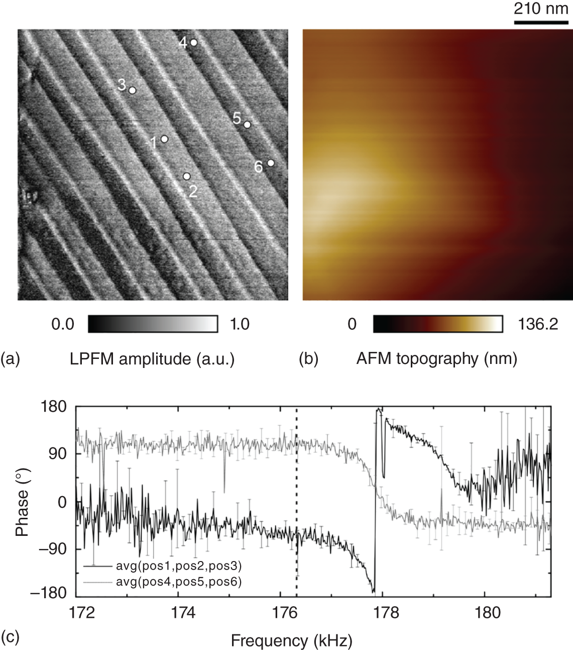
Figure 7.10 (a) Magnified lateral sf‐PFM amplitude of a strictly alternating domain configuration (VAC = 1.1 V). (b) Sample topography for reference. (c) Average of multiple phase responses of a high‐amplitude domain (positions 1, 2, and 3) as well as the average of multiple phase responses of a low‐amplitude domain (positions 4, 5, and 6). The tip–sample resonance frequency remains at 177.8 kHz at all measurement positions, hence excluding changes to the resonance frequency as the origin of the domain contrast. The dashed line indicates the frequency used to measure subfigure (a).
Figure 7.10a depicts a magnified amplitude image of domains recorded in LPFM mode on a MAPbI3 thin film sample. For reference, the corresponding topography is depicted in Figure 7.10b. This sf‐PFM measurement can be validated by measuring the average frequency response of different domains in the sample. The black and gray lines in Figure 7.10c are averaged frequency sweeps of three local phase scans close to the (lateral) contact resonance (here: fRES = 177.8 kHz). Both curves differ by about 180° and show a distinct phase shift at the contact resonance, indicating opposite torsion of the cantilever and hence alternating polarization orientation of the domains at positions 1–3 and positions 4–6. Notably, the error bars of each curve indicate only minor deviations within the particular domain, and no significant change of the resonance frequency is observed, verifying that the 180° phase contrast between domains stems from the piezoresponse of the sample.
It is imperative to note that fabrication methods and hence sample properties often differ from lab to lab. Thus, measurement parameters cannot readily be transferred to other samples or measurement setups but must be adjusted appropriately.
In addition to misinterpretations of artifacts stemming from contact‐resonance enhancement, the PFM signal can be strongly affected by various physical, electrochemical, electrostatic, and capacitive effects [65, 66]. This has led to controversial discussions on the ferroelectric nature of OMH perovskites [60, 61, 67–72]. Many effects must be considered, including piezoresponse, electric currents mediated by semiconductivity and photoconductivity, electrostatic charging, and shifting of mobile ionic charges. External electric fields that are applied in PFM measurements can drive all of these effects. In particular, ion migration and surface charging were suspected to corrupt the PFM signals, concealing the true nature of MAPbI3 [69, 73].
Several groups implemented advanced PFM techniques in order to investigate the true nature of the domains in MAPbI3, to minimize cross talk, to enhance the measurement resolution, and to disentangle all the effects influencing PFM contrast [68, 74].
For example, by using DART‐PFM on MAPbI3 thin films, Vorpahl et al. have obtained similar domain patterns as previously shown with sf‐PFM, avoiding shifts of the resonance frequency and hence supporting the claim of alternating ferroelectric polarization [68]. Huang et al. compared vertical sf‐PFM with vertical DART‐PFM and confirmed alternating domain patterns; however, they concluded that these patterns stem from alternatingly polar and nonpolar domains [74].
Being ferroelectric, the domains disappear when heating MAPbI3 to beyond TC. Figure 7.11a depicts domain patterns in polycrystalline MAPbI3 thin films that vanished upon sample heating to 65 °C (Figure 7.11b) [68]. This coincides with the phase transition of the crystal from tetragonal to cubic. In Figure 7.11c, the domain pattern reappears upon cooling below TC. The recurring domain shape may be a result of pinning and clamping effects [75], where defects and impurities act as seeds for domain formation. These effects are also indicative of the interplay between mechanical strain and polarization, which is typical for ferroelectrics.
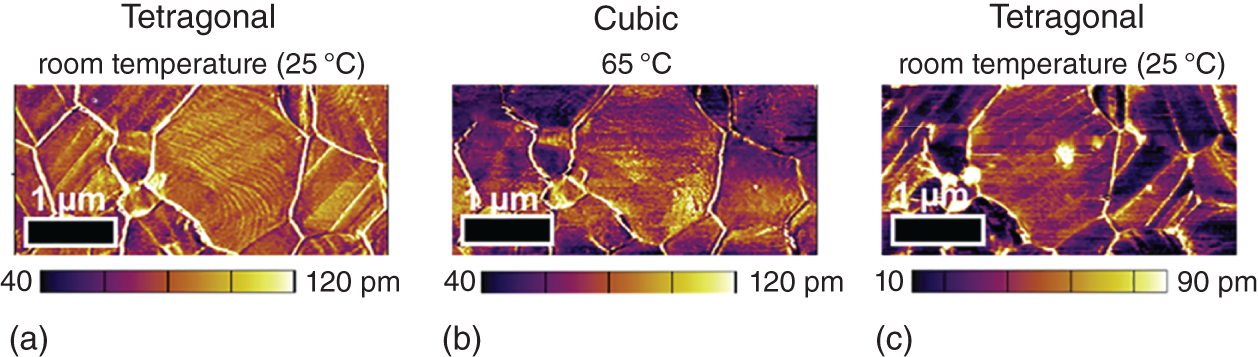
Figure 7.11 Formation and disappearance of domain patterns upon phase transition. (a) DART‐PFM amplitude image of alternatingly polarized domain patterns at room temperature. (b) Upon heating above TC, the domains vanish and the crystal transforms into a cubic structure. (c) After cooling back down to the tetragonal phase, the domains reappear almost identical in size and position, indicating pinning and clamping effects in the polycrystalline thin film.
Source: Reprinted (adapted) with permission from Vorpahl et al. [68]. Copyright (2018) American Chemical Society.
7.3.4 Correlative Domain Characterization
The ferroelectric domains and their properties also show in other experiments using complementary characterization techniques, thereby completing the picture of the ferroelectric properties of MAPbI3 and related microstructural features.
7.3.4.1 Transmission Electron Microscopy
Rothmann et al. investigated polycrystalline MAPbI3 thin films of 300 nm thickness by transmission electron microscopy (TEM) [76]. The TEM image of MAPbI3 in Figure 7.12 shows the same distinct domain patterns that are also observed in PFM images. In TEM, the electrons travel through the sample, interacting with the crystal lattice. Notably, not all grains exhibit strong domain contrast, but some appear rather blurred, which may stem from a tilt of the domain assembly.

Figure 7.12 The domains of polycrystalline MAPbI3 thin film samples also show in transmission electron microscopy (TEM), confirming their bulk character (scale bar, 500 nm).
Source: Reprinted (adapted) with permission from Rothmann et al. [76]. Published under Creative Commons Attribution 4.0 International License (2017).
7.3.4.2 X‐ray Diffraction
X‐ray diffraction (XRD) is the prevalent technique to determine the crystal phase and orientation of a powder or polycrystalline sample. This measurement uses the Bragg condition for constructive interference. If the difference in path length of X‐rays that are diffracted by parallel crystal planes is equal to an integer multiple of the wavelength, constructive interference occurs. Therefore, the characteristic angles at which constructive interference produces diffraction peaks correspond to the spacing of crystal planes. This lattice spacing is specific for the crystal structure and orientation. In the commonly used Bragg–Brentano measurement geometry, the X‐ray source and the detector are held at a constant radius from the sample with the beam focused on the detector. Consequently, at the sample position, the beam is defocused. Simultaneous rotation of the source and the detector by θ relative to the sample plane during the measurement produces X‐ray diffractograms of intensities vs. 2θ with high angular resolution, but typically results in low spatial resolution on the sample.
Jacobsson et al. put the high angular resolution to use by analyzing lattice parameter changes of MAPbI3 across a range of temperatures, including TC [77]. Remarkably, they found a large thermal expansion coefficient of 1.57 × 10⁻⁴ K−1 and determined the phase transition temperature TC from the cubic to the tetragonal phase to 54 °C ± 1 °C.
Another important use of XRD for the investigation of OMH perovskite thin films is the determination of the texture (preferential crystal orientation) of samples. Strong textures often correlate with high‐power conversion efficiencies of perovskite solar cells [78, 79]. Figure 7.13 shows an XRD diffractogram of a MAPbI3 thin film with a (110) texture. The (110) plane is parallel to the c‐axis. Therefore, the c‐axis of the grains and their polarization is oriented in‐plane. Notably, XRD diffraction measurements provide an integrated information of the texture of the sample surface. If local resolution of the crystal orientation at grain size level is required, other diffraction techniques are better suited.

Figure 7.13 XRD diffractogram showing a strong (110) texture of a typical light‐harvesting MAPbI3 thin film as often employed in solar cells.
Source: Reprinted (adapted) with permission from Leonhard et al., DOI: 10.1002/ente.201800989. Copyright (2019) WILEY‐VCH Verlag GmbH & Co. KGaA. Leonhard et al. [80].
7.3.4.3 Electron Backscatter Diffraction
Electron backscatter diffraction (EBSD) can be used to gather spatially resolved crystal orientations with sub‐grain resolution [81]. EBSD utilizes the beam of a scanning electron microscope to probe the crystal lattice of a sample. The interaction with the crystal lattice generates characteristic diffraction patterns that represent the orientation of the crystal lattice planes [82]. By comparing the diffraction patterns to theoretic models, a distinct crystal orientation is assigned to each sample position. EBSD can therefore produce a map of crystal orientations, which correlates with domain patterns probed by PFM measurements. Figure 7.14 shows a typical correlation of EBSD and PFM measurements together with the AFM topography of a polycrystalline MAPbI3 sample [80]. In Figure 7.14b, the vast majority of grains exhibit a (110) crystal orientation (texture), which is in accordance with many reports on XRD measurements of MAPbI3 thin films [83–85]. A (110) crystal orientation is synonymous for the c‐axis of the tetragonal perovskite unit cell being oriented in‐plane. The corresponding PFM images show matching domain patterns: on (110) oriented grains, LPFM images exhibit strong amplitude contrast and distinct phase contrast of 180° (Figure 7.14c,d). VPFM images of the same grains, as exemplified in Figure 7.14e,f, show no or only minor contrast, which may stem from cross talk by cantilever buckling. Very few grains (highlighted) exhibit a tilted orientation relative to the substrate (Figure 7.14b). Concurrently, these grains show a clear domain contrast in VPFM (Figure 7.14e,f). This anisotropy of LPFM and VPFM indicates a predominant in‐plane orientation of the polarization of the majority of grains. Together, these observations allow two important conclusions: Firstly, the polarization correlates with the c‐axis of the tetragonal crystal structure, which is typical for many ferroelectrics and which nicely matches the work by Breternitz et al. on MAPbI3 [34]. Secondly, the few grains that are tilted relative to the substrate plane exhibit both in‐plane and out‐of‐plane polarization components.
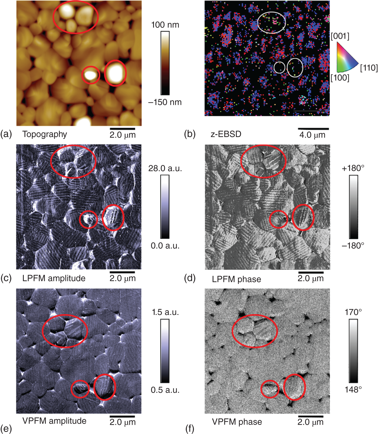
Figure 7.14 Correlative microscopy study combining PFM and EBSD. (a) In the AFM topography image of the polycrystalline MAPbI3 layer, most grains appear with sizes of several micrometers and flat surfaces, while some others protrude from the layer. (b) The EBSD micrograph shows the (110) crystal orientation of flat grain surfaces with high spatial resolution. The protruding grains exhibit a different orientation indicating a tilt of the grains. (c)–(f) LPFM and VPFM amplitude and phase images. Flat grains with (110) orientation do not show any PFM contrast in vertical direction but distinct in‐plane polarization. Tilted grains exhibit both in‐plane and out‐of‐plane polarization.
Source: Reprinted (adapted) with permission from Leonhard et al. [80]. Copyright (2019) WILEY‐VCH Verlag GmbH & Co. KGaA.
7.3.4.4 Kelvin Probe Force Microscopy
If individual grains exhibit alternatingly polarized domains with out‐of‐plane polarization components, the surface potential must be spatially modulated. Such a surface potential modulation can be monitored with Kelvin probe force microscopy (KPFM). Figure 7.15 depicts a correlation of topography, EBSD, LPFM, VPFM, and KPFM of a representative tilted grain surrounded by grains with (110) orientation. The surrounding grains with (110) orientation consistently show 90‐nm‐wide and in‐plane polarized domains in LPFM. The protruding grain in the center of the image has a different orientation and hence a tilted domain assembly. It shows in both LPFM and VPFM, indicating out‐of‐plane polarization components, and the domains are seemingly widened, which is a projection effect of the tilted domain assembly. The out‐of‐plane polarization components locally induce compensating surface charges (screening charges), and hence the contact potential difference (CPD) in the KPFM images is modulated, precisely resembling the domain pattern in the PFM images. These surface charges can be either free charge carriers or ions from the crystal lattice, both of which occur in MAPbI3 [86].

Figure 7.15 Correlative study on the grain orientation in MAPbI3 thin films, the ferroelectric domain polarization, and their influence on surface charges. (a) The central grain protrudes from the surrounding flat grains with diameters of several micrometer. (b) The corresponding EBSD measurement reveals that this grain is tilted while the other grains exhibit a preferential (110) orientation. (c, d) Only the tilted grain exhibits strong contrast in both LPFM and VPFM, indicating in‐plane as well as out‐of‐plane polarization components. At the same time, the domains appear wider due to projection effects on the surface of the tilted grain. (e) The vertical polarization component produces different compensating surface charges, which become visible in the contact potential difference (CPD) in KPFM.
Source: Reprinted (adapted) with permission from Leonhard et al. [80]. Copyright (2019) WILEY‐VCH Verlag GmbH & Co. KGaA.
7.3.5 Polarization Orientation
The data discussed earlier produces a consistent picture of domains with almost exclusive in‐plane polarization on large, flat grains. Yet, the geometry and symmetry of the ferroelectric domain assemblies can provide further information on the polarization direction. Figure 7.16a depicts a characteristic pattern of alternating domains with an in‐plane polarization and a bright contrast in LPFM amplitude. Occasionally, the domains continue at an angle of 90°. To be consistent throughout these alternating domains, the polarization must form a 45° angle toward the domain boundaries as illustrated in Figure 7.16b,c, hence forming 90°‐domains (see Figure 7.2; not to be confused with the continuation angle of 90° of these domains). These 90°‐domains cause the distinct contrast in LPFM amplitude between neighboring domains (180°‐domains with antiparallel in‐plane polarization would create a uniform PFM amplitude).

Figure 7.16 (a) LPFM micrograph of domains with alternating polarization on an individual grain of MAPbI3. The in‐plane polarized domains allow conclusions on the polarization orientation toward the domain boundaries. Two principal domain configurations are possible: (b) head‐to‐tail orientation and (c) head‐to‐head orientation. While head‐to‐tail orientations of ferroelectric polarizations across domains are generally energetically favorable, the low polarization strength of MAPbI3 may allow the occurrence of both.
To date, it remains subject of further research whether these domain assemblies in MAPbI3 exhibit head‐to‐tail or head‐to‐head polarization or if both configurations can coexist. Since both configurations compensate energetically unfavorable charge carrier accumulation and mechanical strain in the polycrystalline layer, they are often referred to as ferroelastic domain configurations in a ferroelectric material [15].
7.3.6 Ferroelastic Effects in MAPbI3 Thin Films
Common ferroelectric materials are also ferroelastic, which is why MAPbI3 is also often described and characterized by its ferroelastic properties. Mechanical stress, e.g. during thin film formation, triggers the formation of 90°‐domains. Strelcov et al. pointed out that mechanical switching of domains by the loading forces of the AFM tip is unlikely to occur during scanning in contact mode, but that the tip would rather damage the layer [60].
Using DART‐PFM, Strelcov et al. observed changes to the domain patterns in MAPbI3 upon application of external mechanic stress [60] The topography and PFM amplitude images in Figure 7.17 show how the shape and amount of domains change in response to mechanical stress.

Figure 7.17 Effects of tensile mechanical stress on the domain patterns in a MAPbI3 single crystal. (a, b) Both the topography and the PFM amplitude of a pristine sample exhibit alternating domains with varying position and width. (c, d) Upon tensile stress, the domain pattern changes to wider but fewer domains. (e, f) When the stress is relieved, some domains retain their shape, but also new domains form. Reprinted with permission of AAAS from [Strelcov et al. [60]]. © The Authors, some rights reserved; exclusive license American Association for the Advancement of Science. Distributed under a Creative Commons Attribution NonCommercial License 4.0 (CC BY‐NC).
Early works on the ferroic properties of MAPbI3 concluded that MAPbI3 is purely ferroelastic (non‐ferroelectric) [60, 67]. Employing PFM, Hermes et al. found domain patterns in MAPbI3; since the authors did not observe clear hysteresis curves switching of the polarization orientation under an externally applied electrical field, they concluded on a ferroelastic nature of the domains [67]. The samples were visible in PFM despite their supposedly non‐ferroelectric character, back then, being attributed to ion migration and charging of surfaces [87].
Jariwala et al. recently reported on the relative orientation of grains in a MAPbI3 thin film by using an advanced EBSD detector to obtain high resolution [75]. In their study, they showed that local variations of the crystal orientation within individual grains of a polycrystalline thin film create local heterogeneities in crystal structure and strain. Especially at grain boundaries, the orientation of individual grains relative to their neighbors can change, which results in local strain. Although Jariwala et al. did not correlate their results to ferroelectric domains, these findings hint at certain mechanisms behind the domain pattern formation in MAPbI3. The mechanical strain that occurs during thin film deposition and drying can determine the orientation of grains and the formation of domains. In light of different sample fabrication procedures in different labs, this would explain and consolidate seemingly inconsistent conclusions in the literature whether MAPbI3 is ferroelectric or purely ferroelastic (non‐ferroelectric) [69–72, 87]. All data discussed here support a combined ferroelectric–ferroelastic nature of MAPbI3.
Although the discussions whether MAPbI3 is ferroelectric or purely ferroelastic (non‐ferroelectric) continue to fill the scientific literature, there is, to date, no holistic theory explaining all the microscopic observations earlier in the absence of ferroelectricity.
7.4 Ferroelectric Poling of MAPbI3
The macroscopic and classical hallmark of ferroelectric materials is their polarizability in an external electric field. While most common ferroelectrics (e.g. BaTiO3) are insulators, the semiconducting nature of MAPbI3 fundamentally changes the methods of characterization and the interpretation of data. The poling of ferroelectric insulators typically requires an external electrical poling field that exceeds the coercive field. Readily applying strong electric fields to the semiconducting MAPbI3, however, would cause significant electric currents and eventually destroy the crystal or thin film. Irrespective of this sample damage, the ionic conductivity and photoconductivity of MAPbI3 would further complicate the characterization.
Ferroelectric poling requires a certain amount of activation energy provided by an electric field in order to switch the unit cells in the crystal lattice from one stable polarization state to the other. Depending on the direction of the electrical field, this transformation may enforce a deformation of the unit cell and hence induce stress and strain in the crystal.
In insulating ferroelectrics, the poling can be tracked by monitoring a current of poling charge carriers, flowing upon ferroelectric switching under a sufficiently strong electric field. In MAPbI3, this ferroelectric switching current is much smaller than the ionic and electronic currents that are driven through the semiconductor by the applied bias. The ionic conductivity increases with temperature and the electronic conductivity increases with generation of free charge carriers under illumination. Unlike the electronic current, the ionic current is limited by the number of free ions or the supply of ions that can be released from the crystal lattice. Therefore, under a DC field, the ionic current must cease at some point while an alternating voltage modulates a continuous ionic current in the sample.
Since both the ionic and electronic currents can damage the MAPbI3 sample during poling, a couple of mitigation strategies exist:
- (1) The contribution of ionic conductivity in MAPbI3 can be reduced by reducing the crystal temperature [8].
- (2) Photoconductivity can be suspended by keeping the sample in the dark [88].
- (3) An alternating electric field, which is applied for a limited duration, can provide the energy that is required for poling, while minimizing the electric currents and hence the thermal damage (AC poling) [89].
- (4) Ferroelectric poling can be accomplished with electric poling fields of reduced magnitude, if the electric field is continuously applied for a longer time. This process is referred to as creeping poling and involves thermally activated shifting of domain walls and domains [90].
- (5) In order to maximize the effect of the electric field on the ferroelectric polarization, ideally, the poling field should be aligned parallel or antiparallel to the polarization dipole of the crystal.
Some of these strategies or combinations thereof have been employed for ferroelectric poling of MAPbI3. For example, following strategy 1, Rakita et al. investigated MAPbI3 single crystals at low temperatures (204 K), where the tetragonal ferroelectric phase still prevails, and recorded a hysteresis curve vs. an electric poling field in the range of ±200 mV/μm [8]. Strategy 3 and a combination of strategies 2, 4, and 5 turned out to be most successful to characterize MAPbI3 at room temperature, which is why they are described in more detail below.
7.4.1 AC Poling of MAPbI3
The most commonly employed technique to probe a sample for ferroelectricity is the application of an AC voltage and the tracking of poling charges through the sample via a reference capacitor.
Common setups for this AC poling of ferroelectrics build on the Tower–Sawyer circuit in Figure 7.18. This circuit comprises a reference capacitance Cref that limits the total amount of charge carriers, which can be driven through the sample during one cycle. By measuring the voltage of this capacitor, the total displacement of charge carriers from both ferroelectric poling and leakage currents can be calculated. In order to ensure that a significant part of the poling voltage Vpol is applied to the sample, Cref must be chosen much larger than Csample. Yet, a smaller reference capacitance allows a more accurate measurement of the total charge during one cycle, hence requiring a careful choice of Cref and Csample.
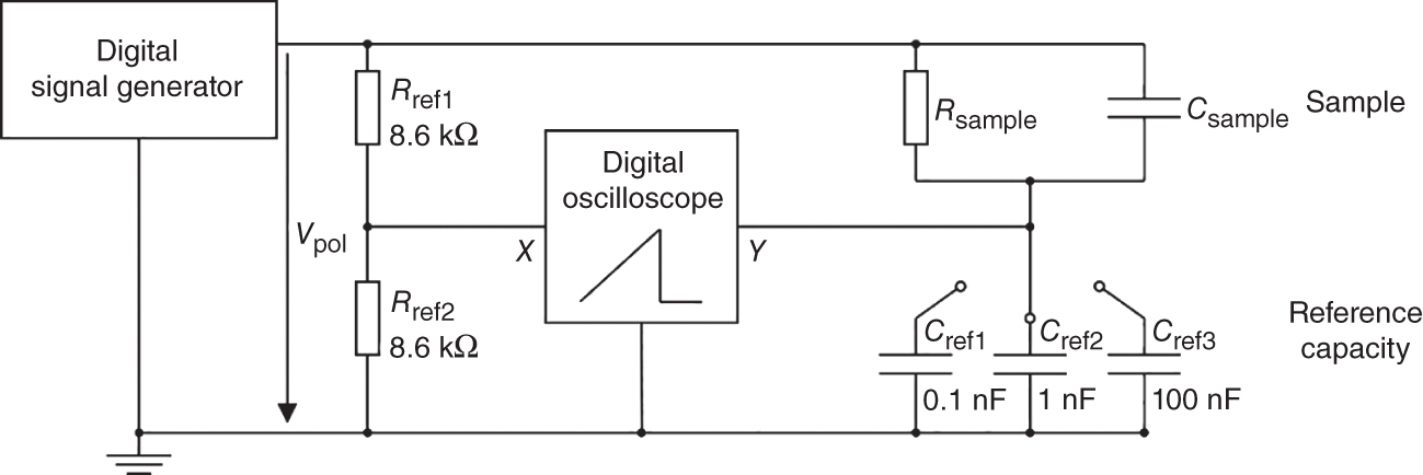
Figure 7.18 Exemplary Tower–Sawyer setup for tracking ferroelectric AC poling.
Source: Röhm [91]. Licensed under CC BY SA‐4.0.
This measurement principle produces best results on insulator samples with a high shunt resistance Rsample because the majority of charge carriers flowing onto the reference capacitor must then stem from poling charges. The reliability of the measurement principle on samples with low shunt resistance, however, is limited. A low shunt resistance can originate from defects in the sample such as pinholes that interconnect both electrodes, from conductive impurities within the sample, or from a high conductivity of the sample itself. In MAPbI3 thin films, all three effects can occur, but its relatively high intrinsic conductivity prevails. According to Fan et al. applying the Tower–Sawyer approach to OMH perovskites can produce sample damage and lead to a misinterpretation of data [59].
Figure 7.19a shows the polarization magnitude P of a MAPbI3 thin film sample that was calculated from the charge on the reference capacitor Cref, assuming a high shunt resistance of the sample. The alternating poling voltage amplitude Vpol was varied between 30 and 90 kV/cm2, leading to a nonlinear increase of the reference capacitor charging. The strong frequency dependence of this charging process cannot be traced to any poling processes within the sample, which would occur on a much shorter timescale, but rather to a low shunt resistance (Figure 7.19b). This is further exemplified by studying the current I through the sample (Figure 7.19c): At an electric field of approximately 20 kV/cm, the current increases exponentially but does not saturate (region 1), and even with decreasing electric field (region 2), the high current is retained, indicating an enhanced sample conductivity and hence a reduced shunt resistance. In contrast, a typical ferroelectric reference (Figure 7.19d) shows a poling current that declines after the switching process, hence producing a characteristic hysteretic ferroelectric polarization curve. This comparison demonstrates the ambiguities in the macroscopic current characteristics under alternating poling voltages, thus not allowing sound conclusions on the ferroelectricity or non‐ferroelectricity of the semiconducting MAPbI3.

Figure 7.19 Challenges of measuring P–E hysteresis loops on a semiconducting, ionic compound such as MAPbI3 using a reference capacitor. (a) While the nonlinear increase of charge carriers through the sample creates a hysteresis loop, (b) the frequency dependency reveals a rather slow charging of the reference capacitor. (c) The sample current shows a hysteresis but no saturation, so that an unadulterated poling current can be excluded. (d) For reference, the hysteresis of a ferroelectric material with a low leakage current (BiFeO3) shows an increase of the current upon ferroelectric switching that decreases afterward. This is synonymous with a saturation of the polarization PS.
Source: Reprinted (adapted) with permission from Fan et al., DOI: 10.1021/acs.jpclett.5b00389. Copyright (2015) American Chemical Society. Fan et al. [59].
7.4.2 Creeping Poling and Switching Events on the Microscopic Scale
Due to its semiconducting nature, electric poling experiments on MAPbI3 require careful design. In contrast to classical insulating ferroelectrics, the non‐negligible sample conductivity can produce dissipative thermal energy from the flow of charge carriers, eventually destroying the sample. The mitigation strategy of choice is creeping poling under small DC voltages over several minutes, which was successfully employed on oxidic perovskites in the past [90]. In creeping poling, the small device currents do not destroy the sample, while the moderate electric field can be used to change the polarization orientation of ferroelectric samples over a longer period of time. By carrying out the experiment in the dark, additional photocurrents can also be avoided for minimal device currents.
For the design of the experiment, further attention must be paid to the polarization direction of MAPbI3 thin films. The (110) texture of most MAPbI3 thin films implies an in‐plane orientation of the c‐axis as well as an in‐plane polarization of the tetragonal unit cell. Therefore, lowest poling fields are expected if the field is applied to the sample in‐plane. For reasons of symmetry, electric fields perpendicular to the crystal polarization do not lead to directional switching in a crystal comprising tetragonal unit cells.
To account for all these boundary conditions, Röhm et al. designed an elaborated poling setup, which is depicted in Figure 7.20 [88]. This sample architecture is commonly used for thin film field‐effect transistors, employing a conductive (n‐doped) silicon wafer with an insulating native silicon dioxide (SiO2) layer and two gold electrodes on top, which are realized in an interdigitated structure. The two gold electrodes allow the lateral application of the poling voltage over a well‐defined poling channel. At the same time, the setup enables PFM measurements before and after each poling process using the conductive silicon wafer as counter electrode. The native SiO2 barrier avoids leakage currents between the two electrodes flowing through the conductive silicon and similarly diminishes parasitic currents through the sample during PFM measurements.
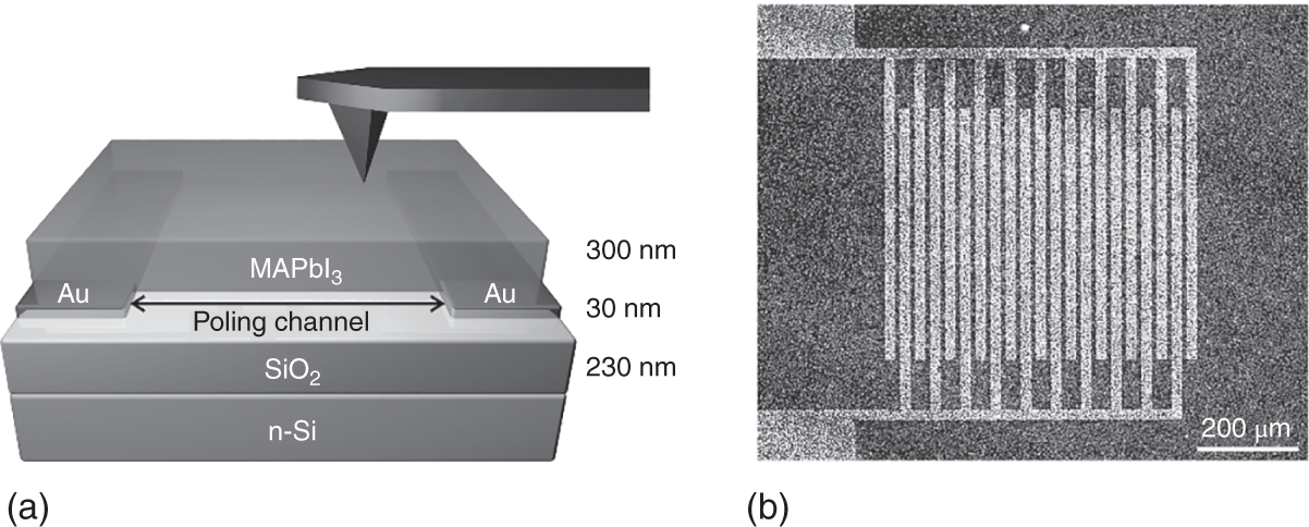
Figure 7.20 (a) Schematic device architecture for the application of lateral poling fields. Two gold electrodes form a poling channel atop an n‐doped silicon wafer, on top of which the MAPbI3 layer is applied. A SiO2 layer isolates the conductive substrate from the electrodes. The conductive substrate can be used as a counter electrode for PFM measurements. (b) Light‐microscopy image of the MAPbI3 layer atop the interdigitated electrodes that form 10 μm wide poling channels.
Source: Reproduced with permission from Dissertation Röhm [91], (CC BY‐SA 4.0).
Figure 7.21a,b depict LPFM measurements on pristine MAPbI3 thin films inside the lateral poling channel at two different positions, before and after applying a lateral DC poling field of 2.0 V/μm for 11 minutes [88]. The red arrow indicates the direction of the electric poling field. Upon application of the poling field, some domains shrunk while others expanded. This effect corresponds to unit cells of the crystal changing their orientation to fit neighboring domains, which is energetically more favorable under the applied bias. Consequently, these energetically more favorable domains grow and domain walls are shifted, which is the hallmark of ferroelectric materials exposed to external poling fields. Similar effects can be observed when reversing the poling direction. Outside the poling channel, above the electrodes, the domain pattern remained unaffected (data not shown here) ruling out any thermal effects to trigger the shaping of domains.

Figure 7.21 (a, b) LPFM measurements at two different positions on a MAPbI3 thin film before (left) and after (right) electric poling by application of a 4.5 V/μm electric field for 11 minutes. (c) The orientation of the AFM cantilever indicates the direction of measurement sensitivity during the scan in subfigures (a) and (b). Areas of bright color represent a significant piezoresponse, where the polarization is perpendicular to the cantilever axis. (d, e) Magnified areas of subfigures (a) and (b), with arrows indicating the polarization configuration. (f) Illustration of the torsion of the AFM cantilever during LPFM measurement.
Source: Reproduced with permission from Dissertation Röhm [91], (CC BY‐SA 4.0).
The static lateral electric field is well defined within the poling channel, allowing conclusions on the reorganization of the orientation of the polarization direction within domains.
The widening and narrowing of domains depend on the orientation of the electric field (red arrow). If domains exhibit polarization components parallel to the electric field, the domains persist and expand. If domains exhibit polarization components antiparallel to the electrical field, the domains or parts thereof change their polarization orientation and hence shrink [92]. This process is illustrated in the magnified sample areas in Figure 7.21d,e. Domains with polarization components that are aligned with the electric field grow, while others shrink. From the changes of the domain dimensions, the polarization direction of domains can be derived as indicated by the gray and white arrows. This interpretation is also in accordance with the theoretic background of PFM measurements: high LPFM amplitudes can only be measured if the piezoresponse of the sample is oriented perpendicular to the AFM cantilever, which is the direction of the highest LPFM sensitivity (Figure 7.21c). Figure 7.21f depicts a schematic of the AFM tip during the LPFM measurement, which is only sensitive to a piezoresponse of the sample perpendicular to the cantilever and hence results in high LPFM amplitude (bright) while sample positions with polarization parallel to the cantilever show only low LPFM amplitude (dark).
7.4.3 Macroscopic Effects of Poling
As demonstrated in Section 7.4.2, creeping poling for several minutes with an electric field of 2 V/μm changes the arrangement of ferroelectric domains in a MAPbI3 thin film. As a consequence of the dipoles having a preferential orientation, screening charges must accumulate at the grain boundaries in order to compensate the potential difference, and the corresponding built‐in electrical field is expected to show in current–voltage sweeps. The sample setup depicted in Figure 7.22 can also be used to monitor the macroscopic effects of poling. Measuring the current through the poling channel while sweeping the poling field between +2 and −2 V/μm produces the I–E characteristic in Figure 7.22a [88]. A strong symmetric hysteresis of the current reveals a change of the sample conductivity at a characteristic electric field of Eon = ±1.6 V/μm. The curve is similar to the characteristics of a Schottky diode for both polarities, which could stem from energetic barriers at the grain boundaries or at the semiconductor–metal interface of the poling channel. Since Eon is independent of the total width of the channel (reported for 2.5, 5, and 10 μm), the former explanation appears more likely. Such a barrier for charge carriers may stem from ionic or electronic screening charges at the grain boundaries of MAPbI3 grains within the poling channel (black outlines in the bottom illustration). Upon creeping poling under +2 V/μm, the current through the channel first rises to 800 nA within 10 seconds and subsequently drops to a stabilized magnitude of 120 nA within several minutes (data not shown here). Afterward, the I–E characteristic in Figure 7.22b changed dramatically: for negative poling fields E, the channel blocks charge carriers, while for positive E, the rising point of the current decreases to Eon = +0.5 V/μm. Similarly, reverse creeping poling under −2 V/μm leads to a stabilized channel current of −120 nA, but unlike poling of the pristine sample, the current starts at low amplitude and slowly rises upon poling (data not shown here). Afterward, the I–E curve is inverted compared with forward poling (Figure 7.22c). This observation led to the conclusion that ferroelectric poling leads to an accumulation of screening charges at the grain boundaries and the metal‐to‐perovskite interface at the electrodes, resulting in an overlap of a remanent polarization and the Schottky diode behavior of the MAPbI3 thin film (Figure 7.22e,f). Hence the sizeable ionic conductivity of OMH perovskites must result in intertwined effects of ferroelectricity, ionic and electronic conductivity.

Figure 7.22 I–E characteristic of the MAPbI3 thin film inside the poling channel as described in Figures 7.20 and 7.21. (a) Before poling, the Au/MAPbI3/Au structure produces symmetric characteristics in forward and backward direction, comparable to a double Schottky diode. (b) After creeping poling for 10 minutes at 2 V/μm, the characteristic becomes asymmetric, similar to the I–E curve of a diode. (c) Similar creeping poling with opposite polarity inverts the characteristic. (d–f) The illustrations underneath each curve show the deductive remanent ferroelectric net polarization of the MAPbI3 grains.
Source: Reproduced with permission from Dissertation Röhm 2019, (CC BY‐SA 4.0). doi: 10.5445/IR/1000099065 [91].
7.5 Impact of Ferroelectricity on the Performance of Solar Cells
7.5.1 Pitfalls During Sample Measurements
The remarkably low electric field under which ferroelectric poling can occur in MAPbI3 raises questions to what extent creeping poling can occur during common device measurements, which would then affect the electric characteristics and eventually the performance of the solar cell [93]. Nearly all J–V sweeps exceed the earlier reported Epol = 2 V/μm. In particular, during maximum power point (MPP) tracking or long‐term stability measurements, such small electric fields are applied to solar cells for a longer period of time.
Röhm et al. applied (vertical) electric fields of ±3 V/μm to MAPbI3 layers in the dark for 10 minutes, which exhibited mostly large grains with predominant in‐plane polarization, sandwiched between the electrodes of solar cells [88]. Before and after the electrical stress, they performed J–V and MPP measurements under illumination. As shown in Figure 7.23, the electric bias produced no notable changes to the solar cell performance after poling. This observation fits very well earlier poling experiments where in‐plane polarized domains could not be switched by vertical electric fields (see Section 7.4.2 for details). However, the situation may be fundamentally different, if the MAPbI3 layer contains domains with out‐of‐plane polarization components as it occurs in layers comprising smaller grains. Then polarization effects may well overlay the photovoltaic response of the solar cell, which would require a careful analysis of the measurement data.

Figure 7.23 J–V characteristics of a typical MAPbI3 solar cell with predominant in‐plane polarization before and after poling for 10 minutes. Neither positive nor negative vertical electric poling fields have a notable influence on the J–V curve.
Source: Röhm, H. (2019). Ferroelektrizität in Methylammoniumbleiiodid‐Solarzellen. Karlsruhe. https://doi.org/10.5445/IR/1000099065. Licensed under CC BY SA‐4.0 [91].
Other effects of unwanted ferroelectric poling are expected to occur during lifetime testing. During accelerated aging tests at elevated temperatures (typically 85 °C [29]), MAPbI3 presents itself in its cubic paraelectric form. Any electric monitoring of the solar cell performance during this test may produce misleading results while the microscopic electric fields of the ferroelectric domains are absent or, at least, the data may be difficult to compare with room temperature aging. This effect may become even more drastic, if the solar cell is subdued to temperature cycling, where a frequent crossing of TC from lower to higher and from higher to lower temperatures occurs together with permanent changes from the ferroelectric to the paraelectric state and back. Notably, the switching from the ferroelectric to the paraelectric state and back may also occur during outdoor operations or under the solar simulator, where TC = 55 °C of MAPbI3 can be exceeded easily.
7.5.2 Charge Carrier Dynamics in Solar Cells
One of the most relevant loss mechanisms in hybrid perovskite solar cells is SRH recombination [94]. SRH recombination occurs at intermediate bandgap states, which stem from defects and impurities in the crystal lattice. Depending on the energetics, electrons or holes can occupy these trap states and hence increase the probability of recombination. Controlling SRH recombination is therefore one of the most important handles to enhance the performance of perovskite solar cells.
To date, no clear experimental picture exists about the charge carrier dynamics in MAPbI3 under influence of ferroelectric polarization. Part of the experimental challenge lies in the convolute of many different material properties that can produce similar macroscopic effects. The fill factor, which is the most important solar cell parameter to describe charge carrier recombination, is a complex parameter. It also unfolds series and parallel device resistance, polarization, and other effects of electrical fields as well as the ideality factor – notwithstanding that more than one recombination mechanism occurs in solar cells. In addition, no experimental evidence exists whether the polarization of neighboring domains is oriented head‐to‐head, producing charged domain walls, or head‐to‐tail, producing uncharged domain walls. In early device simulations, Sherkar and Koster investigated how a ferroelectric polarization might influence the solar cell operation and if it can explain the outstanding performance of perovskites solar cells [7]. They suggested that charged domain walls may locally collect charge carriers from the bulk, driven by the electric field within the ferroelectric domains, and act as charge carrier “highways” to the electrodes. This would directly translate into low recombination losses and enhanced fill factors. However, also uncharged domain walls with head‐to‐tail orientation of the polarization of neighboring domains can assist the charge carrier extraction through separation of charge carriers at a potential step along the domain walls [95]. In a different set of simulations based on experimental domain patterns, Rossi et al. pointed out that only an in‐plane polarization of domains would translate into improved charge carrier separation and extraction, whereas any out‐of‐plane polarization, which is aligned with the electric field between the electrodes, would have no effect [9]. By fitting the corresponding experimental J–V curves of solar cells, taking into account the widely accepted material properties of MAPbI3, they estimated that the polarization strength of MAPbI3 must be on the order of 0.2 μC/cm2. This polarization strength is significantly lower than the polarization strength of most of the classical ferroelectric materials, more difficult to detect, and may therefore partly explain the controversy about the ferroelectric nature of MAPbI3.
References
- 1 Stranks, S.D., Burlakov, V.M., Leijtens, T.J. et al. (2014). Phys. Rev. Appl. 2: 034007.
- 2 Green, M.A., Dunlop, E.D., Hohl‐Ebinger, J. et al. (2020). Prog. Photovolt. Res. Appl. 28: 3–15.
- 3 Wehrenfennig, C., Eperon, G.E., Johnston, M.B. et al. (2014). Adv. Mater. 26: 1584–1589.
- 4 Herz, L.M. (2017). ACS Energy Lett. 2: 1539–1548.
- 5 Seidel, J., Fu, D., Yang, S.‐Y. et al. (2011). Phys. Rev. Lett. 107: 126805.
- 6 Frost, J.M., Butler, K.T., and Walsh, A. (2014). APL Mater. 2: 081506.
- 7 Sherkar, T.S. and Koster, L.J.A. (2016). Phys. Chem. Chem. Phys. 18: 331.
- 8 Rakita, Y., Bar‐Elli, O., Meirzadeh, E. et al. (2017). Proc. Natl. Acad. Sci. U.S.A. 114 (28): E5504–E5512.
- 9 Rossi, D., Pecchia, A., Auf der Maur, M. et al. (2018). Nano Energy 48: 20–26.
- 10 Yang, S.Y., Seidel, J., Byrnes, S.J. et al. (2010). Nat. Nanotechnol. 5: 143–147.
- 11 Nechache, R., Harnagea, C., Li, S. et al. (2015). Nat. Photonics 9: 61–67.
- 12 Fix, T. (2019). Oxide and ferroelectric solar cells. In: Advanced Micro‐ and Nanomaterials for Photovoltaics (eds. D. Ginley and T. Fix), 19–34. Elsevier.
- 13 Jaffe, B., Cook, W.R. Jr., and Jaffe, H. (1971). Piezoelectric Ceramics. London: Academic Press.
- 14 Gross, R. and Marx, A. (2012). Festkörperphysik. München: Oldenbourg.
- 15 Damjanovic, D. (1998). Rep. Prog. Phys. 61: 1267.
- 16 Arlt, G. (1989). Ferroelectrics 91: 3–7.
- 17 Chen, L., Ouyang, J., Ganpule, C.S. et al. (2004). Appl. Phys. Lett. 84: 254.
- 18 Lines, M.E. and Glass, A.M. (1977). Principles and Applications of Ferroelectrics and Related Materials. Oxford: Oxford University Press.
- 19 Arlt, G. (1990). J. Mater. Sci. 25: 2655–2666.
- 20 Wadhawan, V.K. (1982). Phase Transit. 3: 3–103.
- 21 Aizu, K. (1969). J. Phys. Soc. Jpn. 27: 387–396.
- 22 Salje, E.K.H. (2012). Annu. Rev. Mater. Res. 42 (1): 265–283.
- 23 Barsch, G.R. and Krumhansl, J.A. (1984). Phys. Rev. Lett. 53: 1069.
- 24 Aizu, K. (1970). J. Phys. Soc. Jpn. 28: 706–716.
- 25 Schilling, A., Adams, T.B., Bowman, R.M. et al. (2006). Phys. Rev. B 74: 024115.
- 26 Steinhausen, R., Hauke, T., Seifert, W. et al. (1998). Eleventh IEEE International Symposium on Applications of Ferroelectrics ‐ISAF 1998. Proceedings of the Eleventh IEEE International Symposium on Applications of Ferroelectrics (Cat. No.98CH36245), pp. 93–96. Clamping of piezoelectric thin films on metallic substrates: influence on the effective piezoelectric modulus d33.
- 27 Gruverman, A., Auciello, O., Ramesh, R., and Tokumoto, H. (1997). Nanotechnology 8: A38–A43.
- 28 Poglitsch, A. and Weber, D. (1987). J. Chem. Phys. 87: 11.
- 29 Khenkin, M.V., Katz, E.A., Abate, A. et al. (2020). Nat. Energy 5: 35–49.
- 30 Brivio, F., Frost, J.M., Skelton, J.M. et al. (2015). Phys. Rev. B 92: 144308.
- 31 Kojima, A., Teshima, K., Shirai, Y., and Miyasaka, T. (2009). J. Am. Chem. Soc. 131: 6050–6051.
- 32 Stoumpos, C.C., Malliakas, C.D., and Kanatzidis, M.G. (2013). Inorg. Chem. 52: 9019–9038.
- 33 Dang, Y., Liu, Y., Sun, Y. et al. (2015). CrystEngComm 17: 665.
- 34 Breternitz, J., Lehmann, F., Barnett, S.A. et al. (2019). Angew. Chem. Int. Ed.: 1433–7851.
- 35 Baikie, T., Fang, Y., Kadro, J.M. et al. (2013). J. Mater. Chem. A 1: 5628–5641.
- 36 Homes, C.C., Vogt, T., Shapiro, S.M. et al. (2001). Science 293 (5530): 673–676.
- 37 Megaw, H.D. (1952). Acta Cryst. 5: 739.
- 38 Haertling, G.H. (1999). J. Am. Ceram. Soc. 82 (4): 797–818.
- 39 Sharma, H.B., Sarma, H.N.K., and Mansingh, A. (1999). J. Mater. Sci. 34: 1385–1390.
- 40 Frantti, J., Fujioka, Y., Zhang, J. et al. (2014). Rev. Sci. Instrum. 85: 083901.
- 41 Whitfield, P.S., Herron, N., Guise, W.E. et al. (2016). Sci. Rep. 6: 35685.
- 42 Leguy, A.M.A., Frost, J.M., McMahon, A.P. et al. (2015). Nat. Commun. 6: 7124.
- 43 Weller, M.T., Weber, O.J., Henry, P.F. et al. (2015). Chem. Commun. 51: 4180.
- 44 Binnig, G., Quate, C.F., and Gerber, C. (1986). Phys. Rev. Lett. 56: 930.
- 45 Giessibl, F.J. (2003). Rev. Mod. Phys. 75: 949.
- 46 Voigtländer, B. (2015). Scanning Probe Microscopy. Berlin, Heidelberg: Springer‐Verlag.
- 47 Güthner, P. and Dransfeld, K. (1992). Appl. Phys. Lett. 61: 1137.
- 48 Gruverman, A., Auciello, O., and Tokumoto, H. (1998). Annu. Rev. Mater. Sci. 28: 101–123.
- 49 Jungk, T., Hoffmann, A., and Soergel, E. (2008). New J. Phys. 10: 013019.
- 50 Soergel, E. (2011). J. Phys. D: Appl. Phys. 44: 464003.
- 51 Gruverman, A., Alexe, M., and Meier, D. (2019). Nat. Commun. 10: 1661.
- 52 Proksch, R. (2015). J. Appl. Phys. 118: 072011.
- 53 Denning, D., Guyonnet, J., and Rodriguez, B.J. (2016). Int. Mater. Rev. 61: 1.
- 54 Collins, L., Liu, Y., Ovchinnikova, O.S., and Proksch, R. (2019). ACS Nano 13 (7): 8055–8066.
- 55 Strelcov, E., Kim, Y., Yang, J.C. et al. (2012). Appl. Phys. Lett. 101: 192902.
- 56 Rodriguez, B.J., Callahan, C., Kalinin, S.V., and Proksch, R. (2007). Nanotechnology 18: 475504.
- 57 Jesse, S., Mirman, B., and Kalinin, S. (2006). Appl. Phys. Lett. 89: 022906.
- 58 Kutes, Y., Ye, L., Zhou, Y. et al. (2014). J. Phys. Chem. Lett. 5: 3335–3339.
- 59 Fan, Z., Xiao, J., Sun, K. et al. (2015). J. Phys. Chem. Lett. 6: 1155–1161.
- 60 Strelcov, E., Dong, Q., Li, T. et al. (2017). Sci. Adv. 3: e1602165.
- 61 Röhm, H., Leonhard, T., Hoffmann, M.J., and Colsmann, A. (2017). Energy Environ. Sci. 10: 950.
- 62 Garten, L.M., Moore, D.T., Nanayakkara, S.U. et al. (2019). Sci. Adv. 5 (1): eaas9311.
- 63 Hermes, I.M., Best, A., Winkelmann, L. et al. (2020). Energy Environ. Sci. 13 (11): 4168–4177.
- 64 Harnagea, C., Pignolet, A., Alexe, M., and Hesse, D. (2004). Integr. Ferroelectr. 60: 101–110.
- 65 Kalinin, S.V. and Bonnell, D.A. (2002). J. Mater. Res. 17: 5.
- 66 Henrichs, L.F., Bennett, J., and Bell, A.J. (2015). Rev. Sci. Instrum. 86: 083707.
- 67 Hermes, I.M., Bretschneider, S.A., Bergmann, V.W. et al. (2016). J. Phys. Chem. C 120: 5724–5731.
- 68 Vorpahl, S.M., Giridharagopal, R., Eperon, G.E. et al. (2018). ACS Appl. Energy Mater. 1: 1534–1539.
- 69 Liu, Y., Collins, L., Proksch, R. et al. (2018). Nat. Mater. 17: 1013–1019.
- 70 Schulz, A.D., Röhm, H., Leonhard, T. et al. (2019). Nat. Mater. 18: 1050.
- 71 Gomez, A., Wang, Q., Goni, A.R. et al. (2019). Energy Environ. Sci. 12: 2537–2547.
- 72 Colsmann, A., Leonhard, T., Schulz, A.D., and Röhm, H. (2020). Energy Environ. Sci. 13: 1888–1891.
- 73 Vasudevan, R.K., Balke, N., Maksymovych, P. et al. (2017). Appl. Phys. Rev. 4: 021302.
- 74 Huang, B., Kong, G., Esfahani, E.N. et al. (2018). NPJ Quantum Mater. 3: 30.
- 75 Jariwala, S., Sun, H., Adhyaksa, G.W.P. et al. (2019). Joule 3: 1–13.
- 76 Rothmann, M.U., Li, W., Zhu, Y. et al. (2017). Nat. Commun. 8: 14547.
- 77 Jacobsson, T.J., Schwan, L.J., Ottosson, M. et al. (2015). Inorg. Chem. 54 (22): 10678–10685.
- 78 Wang, S., Ma, Z., Liu, B. et al. (2018). Sol. RRL 2: 1800034.
- 79 Jang, G., Kwon, H.‐C., Ma, S. et al. (2019). Adv. Energy Mater. 9: 1901719.
- 80 Leonhard, T., Schulz, A.D., Röhm, H. et al. (2019). Energ. Technol. 7: 1800989.
- 81 Muscarella, L.A., Hutter, E.M., Sanchez, S. et al. (2019). J. Phys. Chem. Lett. 10: 6010–6018.
- 82 Schwartz, A.J. (2000). Electron Backscatter Diffraction in Materials Science. New York: Kluwer Academic.
- 83 Haruyama, J., Sodeyama, K., Han, L., and Tateyama, Y. (2014). J. Phys. Chem. Lett. 5 (16): 2903–2909.
- 84 Yu, H., Wang, F., Xie, F. et al. (2014). Adv. Funct. Mater. 24: 7102–7108.
- 85 Ma, Y., Hangoma, P.M., Park, W.I. et al. (2019). Nanoscale 11: 170.
- 86 Lin, Q., Armin, A., Nagiri, R.C.R. et al. (2015). Nat. Photonics 9: 106–112.
- 87 Liu, Y., Collins, L., Belianinov, A. et al. (2018). Appl. Phys. Lett. 113: 072102.
- 88 Röhm, H., Leonhard, T., Hoffmann, M.J., and Colsmann, A. (2020). Adv. Funct. Mater. 30: 1908657.
- 89 Qiu, C., Wang, B., Zhang, N. et al. (2020). Nature 577: 350–354.
- 90 Gao, Z., Zhang, H., Liu, Y. et al. (2017). Curr. Appl. Phys. 17: 495.
- 91 Röhm, H. (2019). Ferroelektrizität in Methylammoniumbleiiodid‐Solarzellen. Karlsruhe: https://doi.org/10.5445/IR/1000099065.
- 92 Daniels, J.E., Cozzan, C., Ukritnukun, S. et al. (2014). J. Appl. Phys. 115: 224104.
- 93 Colsmann, A. and Röhm, H. (2019). J. Phys. Energy 2: 011003.
- 94 Sherkar, T.S., Momblona, C., Gil‐Escrig, L. et al. (2017). ACS Energy Lett. 2: 1214–1222.
- 95 Liu, S., Zheng, F., Koocher, N.Z. et al. (2015). J. Phys. Chem. Lett. 6: 693–699.