6
Carrier Transport Properties
Hiroyuki Fujiwara and Yoshitsune Kato
Gifu University, Department of Electrical, Electronic and Computer Engineering, 1‐1 Yanagido, Gifu, 501‐1193, Japan
6.1 Introduction
Transport of photo‐generated carriers is a critical factor in the operation of photovoltaic devices [1–3]. For carrier transport in solar cells, the most important physical parameter is carrier diffusion length defined by
where D and τ are the diffusion coefficient and carrier lifetime, respectively [1, 2]. The D is a simple linear function of carrier mobility μ, which is expressed by the Einstein relation:
where kB, T, and q are the Boltzmann constant, temperature, and electron charge, respectively [1, 2]. Note that kBT/q = 25.9 mV at 300 K. Consequently, LD is determined by the pair (μ, τ), and numerous efforts have been made to determine these characteristic values for various hybrid perovskites, including methylammonium lead iodide (CH3NH3PbI3; MAPbI3) [4–35] and formamidinium lead iodide (HC(NH2)2PbI3; FAPbI3) [36–39].
Quite fortunately, hybrid perovskites show favorable high (μ, τ) that lead to large LD (Table 1.1). The LD of the perovskites is sufficiently longer than an absorber layer thickness of ∼500 nm, which is the typical value used for spin‐coated hybrid perovskites. One of the remarkable features of hybrid perovskites is their quite high τ that can be confirmed easily based on photoluminescence (PL) characterization (Figure 1.6 and Chapter 8) [40]. It is now accepted that the long τ observed in hybrid perovskites originates from the absence of deep defects [41, 42]. Specifically, density functional theory (DFT) calculations indicate that the generation of deep traps is energetically unfavorable in MAPbI3 (see Figure 5.17). In fact, trap densities reported for MAPbI3 single crystals are surprisingly low at ∼1010 cm−3 [10, 23, 24]. Some authors argue that the high τ is caused by the indirect‐gap formation (Rashba splitting in the conduction band) [43–47]; however, this is highly unlikely because the direct‐gap formation in the perovskites is evident experimentally (Section 5.4.2).
For the absolute values of (LD, μ, τ) for hybrid perovskites [4–39], however, there is widespread confusion. The intense controversy over hybrid‐perovskite transport properties arises essentially from differences in characterization techniques; namely (μ, τ) depend strongly on how these quantities are measured. Figure 6.1 illustrates the principles of carrier transport characterization by PL, microwave conductivity (MC), terahertz (THz) spectroscopy, and Hall measurements. In the PL, MC, and THz techniques, electron and hole carriers are generated first by short‐wavelength laser pulses, following which the time decay of the photoemission (PL) or the photoconductivity (MC and THz) is characterized (i.e. the optical pump‐probe method). The PL mobility (μPL) is determined analytically from the time decay of the PL intensity [5–7]. The origin of the MC mobility (μMC) and THz mobility (μTHz) is essentially similar, and these are evaluated by using free‐carrier absorption phenomena in the GHz and THz regions. Specifically, free carriers (i.e. free electrons in metals, for example) absorb light particularly in the THz and GHz regions as expressed by the Drude model [48–50]. The variation of the electromagnetic‐wave transmission (or reflection) in the GHz and THz ranges can be related directly to the conductivity [22, 51, 52], from which μ is extracted with a known carrier concentration estimated from the optical‐pump laser pulse [13, 15, 19].
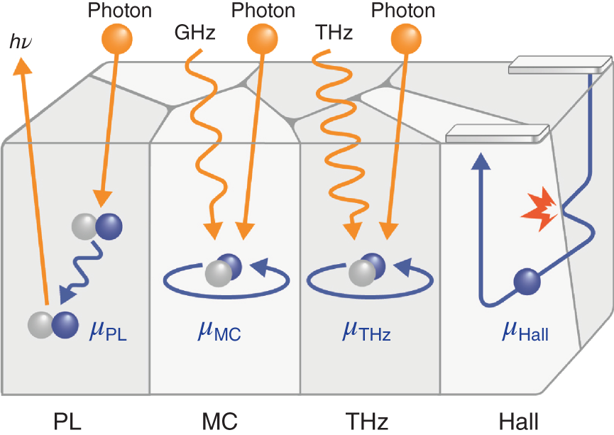
Figure 6.1 Principles of carrier transport characterization by photoluminescence (PL), microwave conductivity (MC), terahertz (THz) spectroscopy, and Hall measurements. The carrier mobility (μ) determined by each method is denoted as μPL, μMC, μTHz, and μHall, respectively. All the noncontact techniques (PL, MC, and THz) characterize carriers excited by short laser pulses. In actual Hall measurements, a total of four or six electrodes are used, although only two electrodes are shown in the figure for simplicity. Note that, for polycrystalline thin films, μMC and μTHz characterize the intragrain mobility without the significant influence of grain boundaries, whereas μHall includes carrier scattering at the grain boundaries.
The PL, MC, and THz methods are noncontact methods and μ can be determined relatively easily. However, μ deduced from these methods includes contributions from both electrons and holes; thus, data interpretation is slightly difficult. In contrast, only one carrier type (i.e. electrons or holes) is characterized in the Hall measurements. Among all the techniques shown in Figure 6.1, the Hall measurement is the most reliable method because the Hall mobility (μHall) can be determined accurately based on the Hall effect [53]. This is the exceptional technique that further allows the simultaneous determination of carrier type (i.e. n‐ or p‐type) and carrier concentration.
Even though the Hall measurement is the favored technique, μHall is affected severely by grain boundaries [49, 54, 55] because the conductivity is measured in the direction perpendicular to the grain boundaries (see Figure 6.1). In contrast, μMC and μTHz are negligibly influenced by grain boundaries, as free carriers do not exist in the region of grain boundaries (see Figure 9.1). Accordingly, when grain boundaries make a significant contribution, we find μTHz > μHall; therefore, comparing μTHz (or μMC) with μHall elucidates the effect of grain boundaries on carrier transport.
In this chapter, we review the carrier transport properties of hybrid perovskites, in an effort to gain consensus on the absolute values of (LD, μ, τ). Section 6.2 explains the carrier properties of hybrid perovskites, using MAPbI3 as an example. We focus on the carrier mobility of MAPbI3 in Section 6.3, which presents controversial physical models to explain what limits the maximum mobility in MAPbI3. Based on the understanding of measurement techniques, we further discuss the appropriate LD of hybrid perovskites (Section 6.4). Section 6.5 explains unique transport properties of various hybrid perovskites.
6.2 Carrier Properties of Hybrid Perovskites
The semiconducting properties of hybrid perovskites arise essentially from the inorganic scaffolds (i.e. PbI3− in APbI3 perovskites), and the unique defect characteristics of hybrid perovskites allow the control of carrier conductivity by the selection of process conditions. This section treats self‐doping in hybrid perovskites by the formation of shallow donor and accepter defects (Section 6.2.1) and discusses its effect on carrier mobility (Section 6.2.2).
6.2.1 Self‐Doping in Hybrid Perovskites
Hybrid perovskites are rarely doped intentionally because the carrier concentration can be varied widely from p‐ to n‐type by so‐called “defect engineering,” in which the carrier properties are controlled by introducing proper defects [9, 56, 57]. Figure 6.2 shows (a) the carrier concentration and the corresponding μHall and (b) the energy separation between the Fermi level (EF) and valence‐band maximum (i.e. ΔE = EF − EVBM) in MAPbI3 thin films as a function of the precursor ratio (PbI2/MAI) [9]. Here, the precursor ratio represents the molar ratio of PbI2/MAI in the precursor mixture solution, adopted for a one‐step spin‐coating process. The results shown in Figure 6.2a,b were obtained from six‐contact Hall measurements with an electrode spacing of ≤1 mm and ultraviolet photoelectron spectroscopy (UPS), respectively. In the figure, the carrier type switches from p to n at the precursor ratio of ∼0.5 and the electron carrier density increases in the PbI2‐rich film. Upon increasing the precursor ratio, the EF position systematically shifts upward due to the enhanced n‐type character [9, 57].
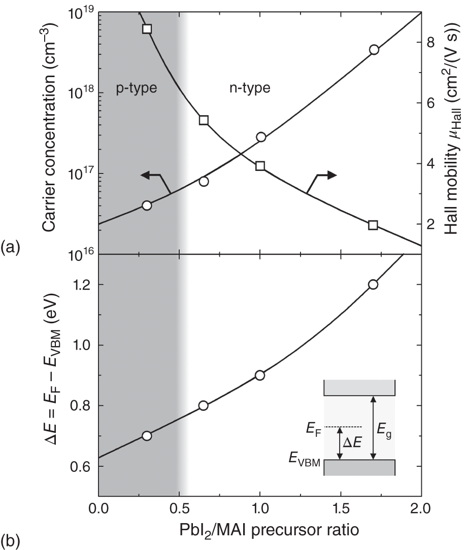
Figure 6.2 (a) Carrier concentration and Hall mobility (μHall) and (b) energy separation between the Fermi level (EF) and valence‐band maximum (i.e. ΔE = EF − EVBM) in MAPbI3 thin films as a function of the precursor ratio (PbI2/MAI) adopted in the thin film formation. The carrier type changes from p‐type to n‐type at PbI2/MAI ∼ 0.5. The lines are to guide the eyes.
Source: Modified from Wang et al. [9].
Importantly, p‐type MAPbI3 films can be converted to n‐type films by thermal annealing at temperatures T ≤ 150 °C [9, 56, 58]. This carrier‐type conversion by annealing originates from MAI desorption from the MAPbI3 surface. Accordingly, it is now widely accepted that MAPbI3 has n‐type conductivity in MAI‐poor (PbI2‐rich) films, whereas p‐type conductivity occurs in PbI2‐poor (MAI‐rich) layers [9][56–59]. Based on DFT results obtained for the point‐defect formation in MAPbI3 (see Figure 5.17), Wang et al. concluded that the n‐type character of MAI‐deficient layers originates from shallow donor formation by I vacancies (VI), whereas p‐type hole generation in the PbI2‐deficient layers occurs because of shallow accepter formation due to Pb vacancies (VPb) [9]. At the present stage, no direct quantitative correlations between defect and carrier densities have been established. Nevertheless, the systematic variation of carrier concentration with the processing condition strongly supports the generation of shallow donor and accepter levels by simple point (or elementary) defects.
The perovskite defects mentioned earlier (VI and VPb) are charged defects (see Figure 5.17) and thus free electrons and holes in the perovskites can be scattered by these defects through the Coulomb interaction (i.e. ionized‐defect scattering). The strong μHall reduction with carrier concentration, shown in Figure 6.2a, can therefore be understood in terms of enhanced carrier scattering by ionized defects.
In Figure 6.2, the carrier properties are shown based on the PbI2/MAI precursor ratio. However, this precursor ratio is only a relative value and the actual Pb/MA ratio in the perovskite layers varies according to (i) growth conditions (deposition methods, solvent) [9, 57], (ii) thermal annealing process [9, 56, 58], and (iii) substrate (or underlying layers) [57]. Thus, the precursor ratio must be considered as a process parameter, rather than as a physical parameter.
For Pb‐based hybrid perovskites, thin layers with low carrier concentrations can be fabricated. Nevertheless, Sn‐based hybrid perovskites often exhibit quite high p‐type carrier densities in the range 1018–1019 cm−3 [60–62]. This significant self‐doping effect has been attributed to the oxidation of the Sn2+ B‐site cation to Sn4+ [63, 64]. In fact, it has been demonstrated that the incorporation of Sn4+ in the form of SnI4 notably enhances p‐type conductivity [65]. Importantly, the stability of the 2+ oxidation state deteriorates as the group‐IV B‐site cation becomes lighter [63]. Thus, Sn2+ in ASnI3 is unstable and is easily oxidized into the more stable Sn4+ state. In photovoltaic devices, high carrier concentrations are quite detrimental and, to reduce the p‐type carrier density in ASnI3 compounds, the additives of SnF2 [62] and Sn metal powders [66] were used.
6.2.2 Effect of Carrier Concentration on Mobility
Figure 6.3 shows μHall as a function of carrier concentration in MAPbI3 [8–10] and MASnI3 [8, 60, 61]. In the figure, the results obtained from bulk crystals (single crystals and polycrystals) and thin films are shown separately. The MAPbI3 bulk crystals show a very low carrier concentration of ∼1010 cm−3 [8, 10], which is significantly less than that in the thin films [9], most likely due to the suppression of the shallow‐defect formation at equilibrium conditions. It can be seen that μHall of MAPbI3 bulk crystals is ∼100 cm2/(V s) and decreases significantly with increasing carrier concentration, independent of carrier type. As discussed in Section 6.3.1, μHall of MAPbI3 thin films decreases in the presence of grain boundaries. However, the result of Figure 6.2 shows a clear trend that μHall of MAPbI3 is also limited by strong carrier scattering by ionized defects, particularly at high carrier concentrations. Thus, LD of MAPbI3 decreases notably at high carrier densities, resulting in reduced solar cell performance. Consequently, the carrier concentration in the perovskite device needs to be controlled properly (see also Section 11.2).
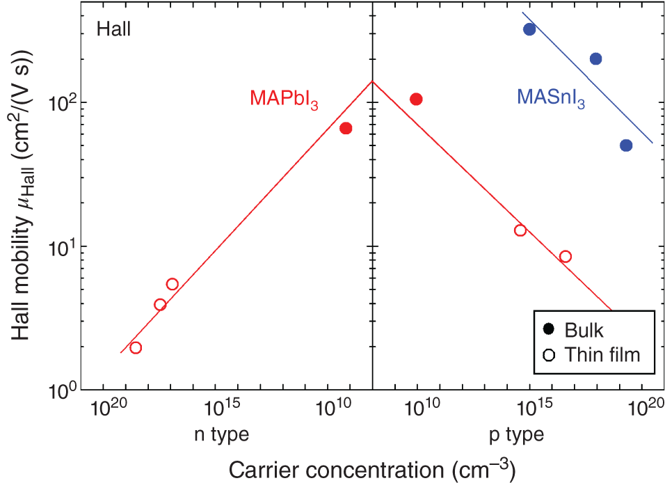
Figure 6.3 Variation of Hall mobility (μHall) with carrier concentration in MAPbI3 [8–10] and MASnI3 [8, 60, 61]. The solid symbols show the results for bulk samples (single crystals and polycrystals), whereas the open circles indicate the results of thin‐film samples. The lines are to guide the eyes. The μHall of the thin films is strongly affected by ionized‐defect scattering and grain‐boundary scattering.
As mentioned earlier, MASnI3 shows strong p‐type character. Rather surprisingly, μHall of MASnI3 bulk crystals is substantially larger than that of MAPbI3 bulk crystals and exhibits >300 cm2/(V s) at the carrier concentration of 1015 cm−3 [8]. Accordingly, μ increases notably when Pb is replaced with Sn. We attribute the higher μHall in MASnI3 to a smaller effective mass in MASnI3 than in MAPbI3 (see Section 6.3.3).
6.3 Carrier Mobility of MAPbI3
The mobility μ is a universal physical parameter that allows for the direct evaluation of carrier transport properties. Nevertheless, the μ reported for MAPbI3 varies in a quite wide range of 0.5–100 cm2/(V s), depending on the sample and characterization method [4–21]. Section 6.3.1 discusses the origin of variation in μ and what is the appropriate μ for MAPbI3. In Section 6.3.2, we see the relationship between the effective mass and μ by making further comparisons with other solar cell materials. The temperature dependence of μ (Section 6.3.3) provides important information on the carrier scattering mechanism in MAPbI3. Based on various results for μ, we discuss what determines the maximum μ of MAPbI3 (Section 6.3.4).
6.3.1 Variation of Mobility with Characterization Method
Figure 6.4 summarizes μ of MAPbI3, as determined by various characterization methods, which are categorized into three groups: (i) PL [5–7], (ii) Hall [8–10], and (iii) MC [11–16] and THz [16–20] measurements. Here, μTHz and μMC are treated as the same group because these methods characterize μ based on the free carrier absorption that occurs primarily within the grains. In other words, μTHz and μMC represent the intragrain mobility without the significant influence of grain boundaries. In addition to the aforementioned methods, μ obtained from a time‐of‐flight (TOF) measurement [21] is also shown in Figure 6.4.
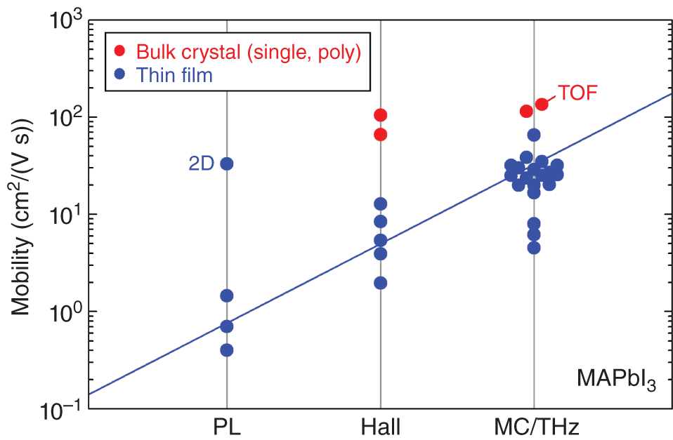
Figure 6.4 Mobility of MAPbI3 determined by various characterization methods, which are categorized into the three groups of (i) PL [5–7], (ii) Hall [8–10], and (iii) MC [11–16] and THz [16–20] measurements. The red circles show the results of the bulk samples (single crystals and polycrystals), whereas the blue circles indicate the results for the thin‐film samples. The plot labeled “TOF” represents μ deduced by using the time‐of‐flight technique [21]. In addition, the PL mobility denoted as “2D” shows that this mobility is determined by the two‐dimensional lateral diffusion of carriers within a MAPbI3 grain [7]. The blue line for the thin‐film results is to guide the eyes.
For MAPbI3 bulk crystals (single crystals and polycrystals), consistent μ values of ∼100 cm2/(V s) (66–135 cm2/(V s)) have been confirmed by Hall [8, 10], MC [15], and TOF [21] measurements, as indicated by the red circles in Figure 6.4. The result of μHall in the figure was evaluated from samples with low carrier concentrations of 1010 cm−3 (see Figure 6.3) and the influence of charged‐defect scattering is minimized. Thus, μ ∼ 100 cm2/(V s) in Figure 6.4 represents the maximum μ of MAPbI3 at room temperature.
In contrast, μ obtained from MAPbI3 thin films (blue circles in Figure 6.4) differs significantly depending on the measurement method; in particular, there exists a clear trend of μMC ∼ μTHz > μHall > μPL. The results of μMC ∼ μTHz show clearly that the intragrain mobility of MAPbI3 thin films is ∼30 cm2/(V s). Note, however, that μMC varies with optical pump intensity (fluence) [11–13, 15, 16], probe microwave frequency [11], and interface structures [11, 14], and thus some ambiguity remains. When bare MAPbI3 samples are probed at the microwave frequency of ∼10 GHz, μMC agrees quite well with μTHz. Quite importantly, in a THz ellipsometry measurement, which characterizes the Drude‐type free‐carrier absorption directly without the pump light, the same μTHz of ∼30 cm2/(V s) is observed [20]. Accordingly, μ ∼ 30 cm2/(V s) can be taken as the maximum intragrain μ in MAPbI3 thin films. This upper limit observed in the thin films (∼30 cm2/(V s)) is much less than that confirmed in the bulk crystal (∼100 cm2/(V s)), indicating that enhanced scattering centers exist within MAPbI3 grains due to imperfect growth of MAPbI3 thin films.
The μHall of polycrystalline thin films is significantly affected by grain boundaries (see Figure 6.1), and μHall of ∼5 cm2/(V s) observed in MAPbI3 is notably lower than μMC and μTHz. In hybrid perovskite thin films, grain sizes exceed the film thickness and there are no grain boundaries along the film‐thickness direction (see Figure 6.1). To represent the vertical carrier transport in the thin‐film devices, therefore, an intragrain μ of 30 cm2/(V s) is appropriate.
The result μPL ∼ 0.5 cm2/(V s) in Figure 6.4 was extracted by assuming a one‐dimensional diffusion model:
where n(x, t), D, and k(t) are the carrier density distribution, diffusion coefficient, and PL decay rate, respectively [5, 6]. The problem of determining μ by PL is that the carrier lifetime tends to be underestimated seriously in this technique. Figure 6.5 shows (a) the time decays of PL and MC signal intensities for a MAPbI3 single crystal [22] and (b) the PL time decays of MAPbI3/quartz, PCBM/MAPbI3/quartz, and spiro‐OMeTAD/MAPbI3/quartz samples [6]. What is striking in Figure 6.5a is that the PL lifetime (τPL < 10 ns) is drastically shorter than the MC lifetime (τMC = 15 μs). The τPL is strongly influenced by interface conditions [5, 6, 67, 68] and, in the example of Figure 6.5b, τPL decreases significantly due to interface formation with the PCBM and spiro‐OMeTAD layers. Importantly, τPL of the bare MAPbI3 sample in Figure 6.5b is governed primarily by surface recombination and τPL improves drastically upon passivating the MAPbI3 surface (Figure 1.6) [40]. As a result, if the nominal short PL decay is adopted for Eq. 6.3, D is seriously underestimated, leading to the drastic reduction in μ. When the lateral diffusion of carriers within a grain is analyzed by PL, however, μPL increases to 33 cm2/(V s) (indicated by “2D” in Figure 6.4) [7], which is consistent with the intragrain μ determined by the MC and THz techniques.

Figure 6.5 (a) Normalized time decays of PL and MC signal intensities for a MAPbI3 single crystal [22] and (b) normalized PL time decays of MAPbI3/quartz, PCBM/MAPbI3/quartz, and spiro‐OMeTAD/MAPbI3/quartz samples[6]. In the figure, the smoothed results of Refs. [6, 22] are shown for clarity. In (a), the MC measurement was made by using a pump laser at 845 nm, whereas the PL was excited at 405 nm. Note that the lifetime tends to decrease when using an excitation laser with a shorter wavelength because carriers are generated nearer the surface due to reduced optical penetration depth.
To investigate μ of MAPbI3, the field effect transistors (FETs) were fabricated [28–32]. Nevertheless, the FET mobilities are surprisingly low (10−5–0.5 cm2/(V s)) [28–31] and thus an accurate determination of μ is difficult from FET measurements, which use quite high applied voltages of <60 V.
6.3.2 Temperature Dependence
Figure 6.6 shows the variation of μTHz in a MAPbI3 thin film with a measurement temperature T, reported in Ref. [19]. The μTHz increases strongly with decreasing T and reaches a high value of 100 cm2/(V s). As explained in Figure 3.13, the crystal structure of MAPbI3 shows distinct phase transitions at 165 K (orthorhombic → tetragonal) and 327 K (tetragonal → cubic). However, no significant discontinuity appears for μTHz as a function of T. This is in sharp contrast with the MA+ reorientation time (Figure 3.16) and the band gap (Figure 4.19), which show irregular discontinuities at the orthorhombic‐tetragonal transition temperature. In other words, the organic cation reorientation and the Pb–I–Pb bond angle change have little effects on μ. The solid line in Figure 6.6 shows the result of fitting to the experimental data and a clear T−1.5 dependence can be seen. Similar variations of μ ∝ Tm with m = −1.8 ∼ −1.4 have been confirmed from PL [7], MC [11, 13], and THz [19] analyses. For μTHz of FAPbI3, different μ variations (m = −1.5 ∼ −0.5) have been reported [38, 39].
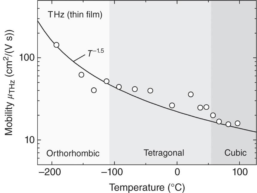
Figure 6.6 Mobility of a MAPbI3 thin film determined by THz measurements (μTHz) as a function of temperature T. The solid line is the fitting result, which shows a clear T−1.5 dependence of the experimental data. The phase transition temperatures of 165 K (orthorhombic → tetragonal) and 327 K (tetragonal → cubic) are also indicated (see also Figure 3.13).
Source: Milot et al. [19]. Licensed under CC BY 4.0.
As known well [1, 2], when μ is limited by lattice scattering, μ decreases with increasing T because stronger lattice vibrations occur at higher T. In contrast, when μ is determined by ionized‐impurity (or defect) scattering, μ increases with T [1, 2], because higher thermal speeds of the carriers at high T reduce the Coulombic interaction between charged scattering center and carrier. The negative exponent observed for μTHz of MAPbI3 (μ ∝ T−1.5) clearly shows that carrier scattering is dominated by thermal‐induced lattice vibrations (see Section 6.3.4 for more discussion).
6.3.3 Effect of Effective Mass
Physically, μ is determined by two factors: (i) an effective mass m* and (ii) a mean time interval between carrier scattering (〈τ〉), as follows [2, 48, 49]:
If there are a large number of defects or scattering centers, the time interval between scattering shortens, thus reducing μ. However, even when the relaxation time 〈τ〉 is same, we observe higher μ for smaller m*. Thus, semiconductors with low m* are quite advantageous in terms of carrier transport. Note that m* is an inherent material value derived from the band structure (Section 5.4.4) and, in semiconductor materials, m* becomes smaller than the electron mass in vacuum (m0) due to the band formation (i.e. m*/m0 < 1).
Table 6.1 summarizes the effective mass of electrons (![]() ) and holes (
) and holes (![]() ), the maximum electron mobility (μe) and hole mobility (μh), and the bulk modulus of representative solar cell materials. The results of
), the maximum electron mobility (μe) and hole mobility (μh), and the bulk modulus of representative solar cell materials. The results of ![]() = 0.32m0 and
= 0.32m0 and ![]() = 0.36m0 for MAPbI3 correspond to the results of DFT in Table 5.3 [70], whereas μe and μh of MAPbI3 indicate μHall in Figure 6.3 [8, 10]. All other values in Table 6.1 are taken from Ref. [69]. The bulk modulus shows how a material compresses under external pressure and represents the hardness (or softness) of materials. It can be seen that MAPbI3 is a very soft material (Table 1.1) [69][71–73].
= 0.36m0 for MAPbI3 correspond to the results of DFT in Table 5.3 [70], whereas μe and μh of MAPbI3 indicate μHall in Figure 6.3 [8, 10]. All other values in Table 6.1 are taken from Ref. [69]. The bulk modulus shows how a material compresses under external pressure and represents the hardness (or softness) of materials. It can be seen that MAPbI3 is a very soft material (Table 1.1) [69][71–73].
Table 6.1 Effective masses of electrons (![]() ) and holes (
) and holes (![]() ), electron mobility (μe) and hole mobility (μh), and bulk moduli of representative solar cell materials.
), electron mobility (μe) and hole mobility (μh), and bulk moduli of representative solar cell materials.
Source: Egger et al. [69].
| Material | μe (cm2/(V s)) | μh (cm2/(V s)) | Bulk modulus (GPa) | ||
|---|---|---|---|---|---|
| Si | 0.32 | 0.54 | 1500 | 500 | 98 |
| GaAs | 0.06 | 0.53 | 8000 | 400 | 75 |
| CdTe | 0.11 | 0.72 | 1100 | 100 | 42 |
| CuInSe2 | 0.16 | 1 | 150 | 20 | 75 |
| MAPbI3 | 0.32 | 0.36 | 66 | 105 | <20 |
All the numerical data were taken from Ref. [69], except for the effective mass [70] and mobility [8, 10] of MAPbI3 (see Table 5.3 for m* of MAPbI3).
Figure 6.7 shows the variation of μ with ![]() and
and ![]() obtained from Table 6.1. This figure contains a plot for MASnI3 that is based on the results of Refs. [8, 74, 75]. All the tetrahedral‐bonding semiconductors show the trend of
obtained from Table 6.1. This figure contains a plot for MASnI3 that is based on the results of Refs. [8, 74, 75]. All the tetrahedral‐bonding semiconductors show the trend of ![]() <
< ![]() and thus μe > μh. In particular, for these materials, due to the large difference between
and thus μe > μh. In particular, for these materials, due to the large difference between ![]() and
and ![]() , μh is significantly less than μe. In contrast, MAPbI3 has the unique property of
, μh is significantly less than μe. In contrast, MAPbI3 has the unique property of ![]() ∼
∼ ![]() and thus we find μe ∼ μh. In solar cells, since both electron and hole carriers need to be collected, well‐balanced μe ∼ μh in MAPbI3 provides a great advantage for efficient carrier collection. Nevertheless, the maximum μe and μh of MAPbI3 (∼100 cm2/(V s)) are rather low. Comparing μe values for Si and MAPbI3 shows that μe of MAPbI3 is one order of magnitude smaller, even though both materials have similar
and thus we find μe ∼ μh. In solar cells, since both electron and hole carriers need to be collected, well‐balanced μe ∼ μh in MAPbI3 provides a great advantage for efficient carrier collection. Nevertheless, the maximum μe and μh of MAPbI3 (∼100 cm2/(V s)) are rather low. Comparing μe values for Si and MAPbI3 shows that μe of MAPbI3 is one order of magnitude smaller, even though both materials have similar ![]() ∼ 0.3m0. The reason for low μ in MAPbI3 is discussed in Section 6.3.4.
∼ 0.3m0. The reason for low μ in MAPbI3 is discussed in Section 6.3.4.
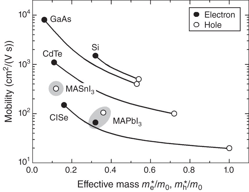
Figure 6.7 Variation of mobility (μ) with  /m0 (closed circles) and
  /m0 (open circles), obtained from Table 6.1. The results for MASnI3 are taken from Refs. [8, 74, 75]. The gray areas highlight the results of MABI3 (B = Pb2+, Sn2+). For inorganic semiconductors, the plots for the electrons and holes are connected by curves for clarity. Note that the result of MAPbI3 is unique in that
  ∼
∼  , which leads to well‐balanced electron and hole mobilities of μe ∼ μh.
We have seen in Figure 6.3 that μh of MASnI3 is substantially larger than that of MAPbI3. This result can be interpreted from a lower ![]() of MASnI3 (see Figure 6.7), which in turn increases μ according to Eq.
6.4. Thus, the effect of m* is significant in hybrid perovskite materials.
of MASnI3 (see Figure 6.7), which in turn increases μ according to Eq.
6.4. Thus, the effect of m* is significant in hybrid perovskite materials.
6.3.4 What Determines Maximum Mobility of MAPbI3?
The experimental μ of MAPbI3 described earlier reveals the important facts that (i) the maximum μ of nondoped MAPbI3 single crystals at room temperature is ∼100 cm2/(V s), (ii) the intragrain μ of MAPbI3 thin films at room temperature is ∼30 cm2/(V s), and (iii) the T dependence of μ is μ ∝ T−1.5. The μ in semiconductor materials is influenced by a variety of factors and, by incorporating carrier scattering models proposed for MAPbI3 [76–88], the experimental μ of hybrid perovskites can be expressed as
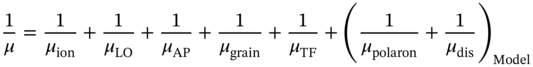
The above equation is based on Matthiessen's rule [2], which indicates that the observable μ is given by the inverse relation and is limited by the lowest μ factor. The major factors determining μ in semiconductors include ionized‐impurity scattering (μion) [1, 89], longitudinal optical (LO) phonon scattering (μLO) [76–80], acoustic phonon scattering (μAP) [1][81–83], and grain‐boundary scattering (μgrain) [49, 54, 55]. In Eq. 6.5, μTF is incorporated to express the reduced μ in the perovskite thin films. The two terms denoted as “Model” represent the proposed scattering mechanisms of polaron formation (μpolaron) [84–86] and anharmonic structural disorder (μdis) [69, 87], as explained below.
When carrier density is low, the value of μion becomes quite large [1, 89] and the term 1/μion vanishes (i.e. 1/μion → 0). In single crystals of MAPbI3 with low carrier densities, the terms 1/μion, 1/μgrain, and 1/μTF disappear. Moreover, DFT calculations show that μAP of MAPbI3 is quite high (>1500 cm2/(V s)) [81–83] and 1/μAP is also eliminated. Consequently, several studies have proposed that the maximum μ is determined by μLO (i.e. μ ∼ μLO in Eq. 6.5) [76–80]. Note that LO phonons displace the atomic positions in a way that can create local electric fields, which further scatter free carriers through strong Coulomb interactions. This coupling between LO phonons and free carriers is referred to as the Fröhlich interaction. The strength of the electron–phonon coupling can be expressed by a dimensionless Fröhlich parameter α [77, 84]:
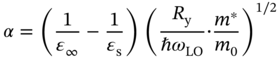
where ε∞ and εs show high frequency and static dielectric constants (see Figure 4.2). The quantities Ry, ℏ, c, and ωLO are the Rydberg constant (Ry = 13.6 eV), Dirac's constant, speed of light, and LO–phonon frequency. The prefactor (1/ε∞ − 1/εs) reflects the effect of the ionic screening.
As explained in Chapter 4, MAPbI3 shows unique phonon absorption characteristics, including (i) quite strong phonon absorption, which leads to εs ≫ ε∞ (Figure 4.2) and (ii) very low peak frequency of ωLO (Figure 4.7). These specific features lead to a quite high coupling constant α, which is estimated to be 1.72–2.68 in MAPbI3 [77, 84, 85]. This value is significantly larger than those of tetrahedral‐bonding semiconductors, such as GaAs (α = 0.07) and CdTe (α = 0.31) [90], and is comparable to crystals with high ionicity, including AgCl (α = 1.8) and KI (α = 2.5) [90]. Accordingly, the LO–phonon coupling in the hybrid perovskite is indeed strong and μLO likely governs the room temperature μ of MAPbI3. Theoretical attempts show that the maximum μLO ranges from 30 to 200 cm2/(V s) with a T dependence of T−1.37 to T−1.5 [78–80].
To explain the maximum μ of ∼100 cm2/(V s) in MAPbI3, two different models have been proposed further: (i) the formation of polarons [84–86] and (ii) carrier scattering by anharmonic lattice vibration [69, 87]. The physical pictures of these models are shown in Figure 6.8. When a hole conducts inside a polar (ionic) semiconductor, for example, the positive charge of the hole attracts anions, while expelling the cations in the opposite direction. Thus, a conduction hole (or electron) displaces the constituent ions from their equilibrium positions, creating a quasiparticle called a polaron (Figure 6.8a). The formation of a polaron lowers μ through a widespread lattice deformation, which can be interpreted as an increase in m*. The polaron effective mass (mp) is derived from the Fröhlich parameter α and mp increases with α [84, 85]. For MAPbI3, mp is 28–64% heavier than m* [84–86] and the polaron‐limited mobility (μpolaron in Eq. 6.5) is estimated to be 133–200 cm2/(V s) [84, 85]. The corresponding polaron radii range from 26 to 51 Å [84, 85]. However, although μpolaron quantitatively agrees with the maximum μ of ∼100 cm2/(V s) at room temperature, the theoretical calculation shows a T dependence of μpolaron ∝ T−0.46 [85]. Thus, μ variation for T is underestimated with the polaron concept.
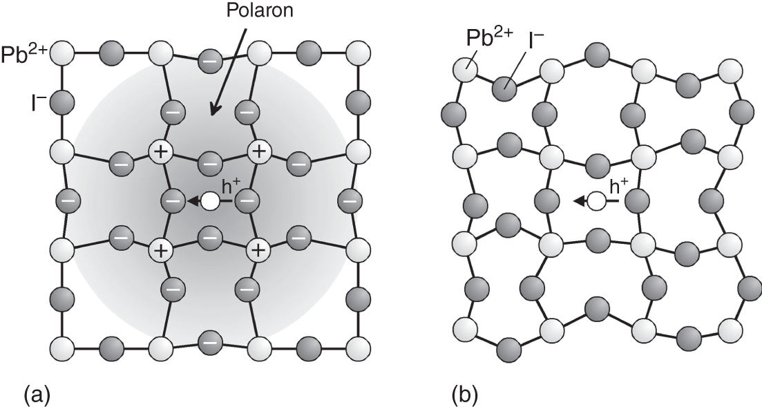
Figure 6.8 Physical pictures of (a) polaron formation and (b) carrier scattering by anharmonic lattice vibrations in MAPbI3. The h+ in the figure indicates a hole. In (a), the hole carrier conduction inside a polar (ionic) semiconductor displaces cations and anions through the Coulomb interaction, creating a quasiparticle called a polaron. In (b), carriers in MAPbI3 are scattered by anharmonic (disordered) vibrations of the PbI3− inorganic cage, as proposed in Refs. [69, 87].
If the PbI3− cage deforms anharmonically, a local potential fluctuation is created, scattering carriers (see Figure 6.8b). A molecular‐dynamics‐based calculation shows that the maximum μe of MAPbI3, limited by such an anharmonic lattice disorder (μdis in Eq. 6.5), is ∼135 cm2/(V s) with the T dependence of ∼T−2 [87]; thus, this model provides the correct transport parameters for MAPbI3. It has been argued that carrier scattering by dynamic lattice disorder becomes particularly important in compounds with “soft lattices” [69, 87] (see bulk modulus in Table 6.1).
All the above discussions, however, are based on a quite simple assumption that μ is determined totally by a single scattering mechanism. In the LO–phonon scattering model, for example, μ(T) = μLO(T) is assumed in Eq. 6.5. However, this is highly doubtful, because the T dependence of μ(T) ∝ T−1.5 is reported for MAPbI3 thin films [7, 11, 13, 18, 19], in which the intragrain μ is lowered by μTF and μion. In particular, it is likely that the intragrain μ of MAPbI3 thin films (∼30 cm2/(V s)) is described by 1/μ = 1/μion + 1/μTF + 1/μLO, or other similar models. Accordingly, more quantitative experimental data, including μ(T) of single crystals, are necessary to conclude the absolute limiting factor of μ in MAPbI3 at room temperature. We mention, however, that the strong LO–phonon carrier scattering is quite likely because the LO–phonon absorption is extraordinarily strong in hybrid perovskites, leading to a large Fröhlich parameter.
6.4 Diffusion Length
One of the greatest advantages of hybrid perovskite solar cells is long LD of carriers [10][13–15, 19][22–27]. Nevertheless, absolute LD values differ significantly depending on the characterization technique. Table 6.2 summarizes LD in MAPbI3 single crystals and thin films, together with their corresponding μ and τ. Figure 6.9 further summarizes the relation of μ and τ for the values of Table 6.2. For the single crystals, LD varies in a range of 8–175 μm, while LD of the thin films is 0.1–23 μm.
Table 6.2 Carrier diffusion length (LD), lifetime (τ), and mobility (μ), reported for MAPbI3 single crystals [10, 15][22–24] and thin films [5, 6, 13, 14, 19][25–27].
| Method | LD (μm) | τ (μs) | μ (cm2/(V s)) | References |
|---|---|---|---|---|
| Single crystal | ||||
| TPVa) | 175 | 82 | 105 | [10] |
| MC | 55 | 10 | 115 | [15] |
| MC | 50 | 15 | 64.5 | [22] |
| SPCMb) | 10–28 | [15] | ||
| TAc) | 10 | 0.57 | 67.2 | [23] |
| PL | 8 | 9.9 | 2.5 | [24] |
| Thin film | ||||
| Opt‐Halld) | 23 | 30 | 8 | [25] |
| MC | 9 | 5 | 6.2 | [13] |
| MC | 4.1 | 0.22 | 30 | [14] |
| THz | 2.5 | 0.07 | 35 | [19] |
| IMPSe) | 1.2–1.5 | [26] | ||
| EBICf) | 1 | [27] | ||
| PL | 0.13 | 0.005 | 1.45 | [6] |
| PL | 0.13 | 0.01 | 0.66 | [5] |
The characterization results obtained from various techniques are summarized. Some of the τ and μ values are calculated by applying the relations of Eqs. (6.1) and (6.2).
aTransient photovoltaic spectroscopy.
bScanning photocurrent microscopy.
cTransient absorption spectroscopy.
dOptical Hall measurement.
eIntensity‐modulated photocurrent/photovoltage spectroscopy.
fElectron‐beam‐induced current technique.
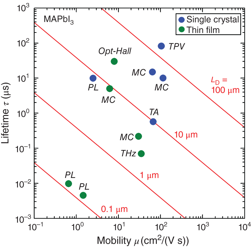
Figure 6.9 Carrier mobility μ and carrier lifetime τ for each characterization of MAPbI3, obtained by using different techniques summarized in Table 6.2. The blue circles show results reported for the single crystals [10, 15][22–24], whereas the green circles indicate results obtained from the thin‐film samples [5, 6, 13, 14, 19, 25]. The red lines indicate the constant‐LD lines obtained for LD = 0.1, 1, 10, and 100 μm, calculated from Eqs. 6.1, 6.2.
In Figure 6.9, we can confirm μ ∼ 100 cm2/(V s) for MAPbI3 single crystals, even though the PL result shows much lower μ, as discussed earlier. In other words, the large variation in LD observed for the single crystals originates from the variation in τ. The MC measurements consistently show τ ∼ 10 μs [15, 22], whereas the transient photovoltaic (TPV) measurements [10] and transient absorption (TA) spectroscopy [23] give different τ values. On the other hand, LD can be determined directly from spatially resolved techniques, including scanning photocurrent microscopy (SPCM) [15] and the electron beam‐induced current (EBIC) technique [27]. The SPCM characterization of MAPbI3 single crystals results in LD of 10–28 μm [15], which is consistent with ∼50 μm determined by MC [15, 22]. Accordingly, LD ∼ 50 μm with μ ∼ 100 cm2/(V s) and τ ∼ 10 μs can be considered as a representative LD of MAPbI3 single crystals.
For MAPbI3 thin films, we observe μ = 10–30 cm2/(V s), with μPL ∼ 1 cm2/(V s), which are consistent with the results of Figure 6.4. However, τ reported for the thin films is quite different (τ = 5 × 10⁻³–30 μs in Table 6.2), most likely due to the strong influence of interfaces in the thin‐film geometry. The τPL is particularly sensitive to the interface (see Figure 6.5b) and the PL technique seriously underestimates LD. The direct characterization of LD in MAPbI3 thin‐film solar cells has been performed by EBIC, resulting in LD ∼ 1 μm [27]. The MC results of the thin films provide LD in a similar range (LD ∼ 5 μm) [14]. Accordingly, LD of 1–5 μm appears to be appropriate for MAPbI3 thin films. Nevertheless, an extremely long τPL of 8 μs has been reported for a MAPbI3 thin film with optimized surface [40] (see Figure 1.6). If τPL = 8 μs and μ = 30 cm2/(V s) are applied, we obtain LD ∼ 25 μm, which is comparable to that of the single crystals. Thus, the LD of 4–23 μm is shown in Table 1.1.
It should be emphasized that the above LD sufficiently exceeds the absorber thicknesses of MAPbI3 solar cells (300–500 nm). In this condition, the effect of carrier recombination within the bulk component becomes less significant and the interface recombination becomes more important. In fact, the open‐circuit voltage (Voc) of hybrid perovskite solar cells depends critically on the interface structure (see Section 11.5.1). Accordingly, it can be concluded that the carrier transport characteristics of MAPbI3 thin films are quite satisfactory, which is one of the main reasons why solar cells with over 20% efficiencies can be fabricated using MAPbI3 as a light absorber (Chapters 1 and 11).
6.5 Carrier Transport in Various Hybrid Perovskites
A variety of perovskite compounds and alloys have been used to fabricate hybrid perovskite solar cells. Here, we see the carrier transport properties of representative perovskite materials. Figure 6.10 summarizes μTHz values reported for various Pb‐based hybrid perovskite thin films [17–19, 37][91–94]. In the figure, the maximum and minimum ranges of μTHz reported for each material are indicated by bars. This result shows an important result; the upper limit of μTHz is ∼30 cm2/(V s) for all the perovskite thin films. Based on the discussion of Section 6.3.4, the observed limit on μTHz could be expressed as
Moreover, μTHz values for MAPbI3 [19], FAPbI3 [37], and Cs0.17FA0.83PbI3 [92] are quite similar, confirming that the effect of the A‐site cation is essentially negligible.
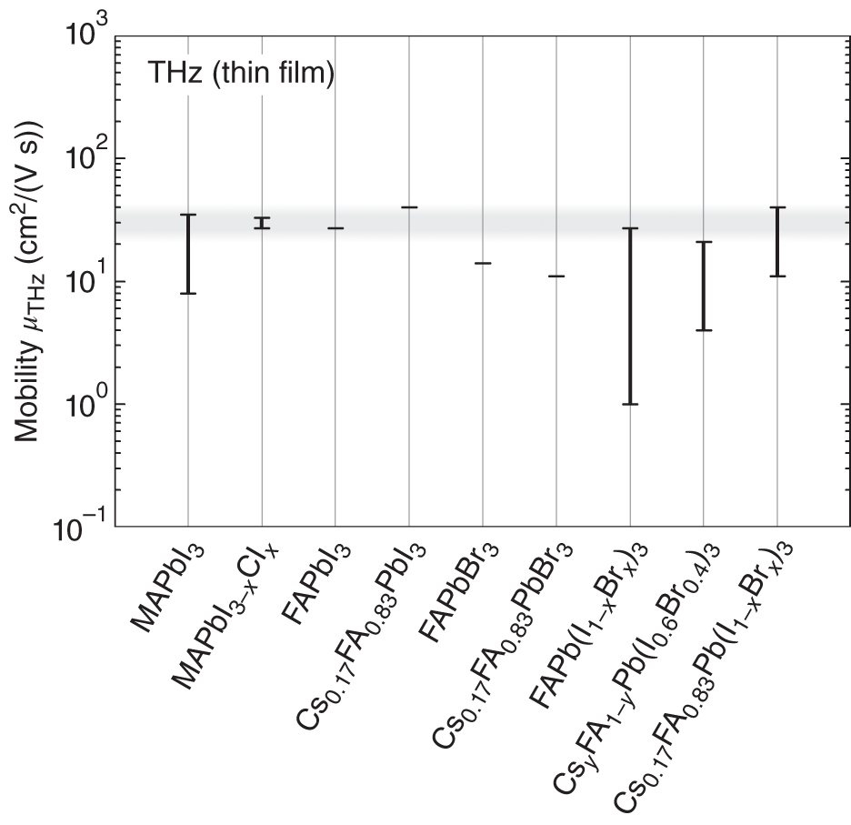
Figure 6.10 Mobility of Pb‐based hybrid perovskite thin films, as determined by THz spectroscopy (μTHz). In the figure, the maximum and minimum ranges of μTHz reported for each material [17–19, 37][91–94] are indicated by the bars. The gray region represents the possible upper limit of μTHz ∼ 30 cm2/(V s) for hybrid perovskite thin films.
Source: Wehrenfennig et al. [17]; Karakus et al. [18]; Milot et al. [19]; Rehman et al. [37]; Wehrenfennig et al. [91]; Rehman et al. [92]; McMeekin et al. [93, 94].
Nevertheless, the A‐site cation affects μ indirectly through the perovskite crystal stability. Figure 6.11 shows (a) μTHz and the width of the (100) X‐ray diffraction (XRD) peak and (b) tolerance factor (t), as a function of the Cs content y in CsyFA1−yPb(I0.6Br0.4)3 thin films. The result of Figure 6.11a is taken from Ref. [92], whereas t in Figure 6.11b is calculated by using Eq. (3.1) with the values of Table 3.3. It can be seen from Figure 6.11a that the crystallinity of the CsFAPb(I,Br)3 alloys improves notably upon the slight incorporation of Cs (y ∼ 0.2) into FAPb(I,Br)3, as evidenced by the sharper XRD peak. More importantly, the crystallinity confirmed by XRD shows an almost perfect correlation with the transport characteristics and μTHz reaches a maximum when the peak width is minimized.
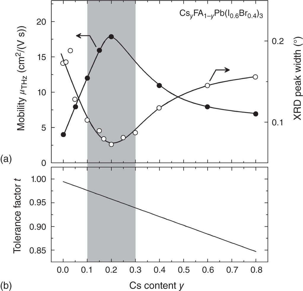
Figure 6.11 (a) μTHz and XRD width of a (100) peak and (b) tolerance factor (t), as functions of the Cs content y in CsyFA1−yPb(I0.6Br0.4)3 thin films. The t in (b) is calculated by using Eq. (3.1) with the values given in Table 3.3. The gray region shows the optimum t range of t = 0.91–0.98, as established in Figure 3.10.
Source: (a) Adapted from Rehman et al. [92].
The high μTHz and small peak width at y ∼ 0.2 can be interpreted by t, which is a global indicator that describes the stability of perovskite crystals (Section 3.3). For Pb‐based hybrid perovskites, t = 0.945 is an ideal value (Figure 3.10), allowing the formation of the stable perovskite phase. Note that secondary‐phase materials, such as PbI2, δ‐CsPbI3, and δ‐FAPbI3 (see Figure 3.5), form when t deviates largely from the optimum t range of 0.91–0.98 (Figure 3.10), as indicated in Figure 6.11. For CsFAPb(I0.6Br0.4)3, t ∼ 0.95 is obtained when y = 0.24 (Figures 6.11b and 3.11c). Thus, the Cs content of y ∼ 0.2 not only provides higher crystallinity but also prevents the inclusion of the secondary phase. Moreover, τPL improves at this Cs composition [92]. As a result, the proper control of the A‐site cation species is critical for the improvement of μTHz and LD. Note that the variation of μTHz in CsFAPb(I,Br)3 thin films can best be represented by μTF in Eq. 6.7, provided that the crystallinity of the single crystals is much better than that of the thin films.
For the variation of the Br content x in FAPb(I1−xBrx)3 and Cs0.17FA0.83Pb(I1−xBrx)3 thin films, a large change in μTHz is also reported (Figure 6.12) [37, 92]. In the case of FAPb(I1−xBrx)3 thin films, μTHz has a minimum value of ∼1 cm2/(V s) at x = 0.3–0.4, which is attributed to the formation of an amorphous phase in this region. The μTHz of Cs0.17FA0.83Pb(I1−xBrx)3 also varies strongly with x. For this alloy, μTHz decreases monotonically from 40 to 11 cm2/(V s) with increasing x. This reduction is suggested to originate from the strong LO–phonon scattering in Br‐based perovskite compounds [4]. However, μ of a MAPbBr3 single crystal evaluated from the TOF measurement (115 cm2/(V s) in Ref. [24]) is comparable to μTOF of a MAPbI3 single crystal (135 cm2/(V s) in Figure 6.4). In addition, the Fröhlich parameter of MAPbBr3 (α = 1.69) is almost the same as that of MAPbI3 (α = 1.72) [84]. Accordingly, μ reduction by the Br incorporation is not evident in MAPbX3. The Br content has negligible effect on t in Cs0.17FA0.83Pb(I1−xBrx)3 (see Figure 3.11). Since the absolute μTHz at x = 1.0 is rather small (11 cm2/(V s)), it is possible that μTF or μion plays a dominant role in the carrier scattering of the Cs0.17FA0.83PbBr3 thin film. For the increase of x in these thin films, the large reduction in LD from 4.4 μm (x = 0) to 0.8 μm (x = 1) is also confirmed [92].
![Schematic illustration of μTHz for{FAPb(I$_{1 - extit{x$Br$_ textit{x$)$_{3}$ thin films FAPb(I1-xBrx)3 and Cs0.17FA0.83Pb(I1-xBrx)3 thin films{Cs$_{0.17}$FA$_{0.83}$Pb(I$_{1- extit{x$Br$_ textit{x$)$_{3}$ thin films as a function of the Br content x, reported in Refs. [37, 92]. The very low μTHz observed at x = 0.3-0.4 in FAPb(I1-xBrx)3 has been attributed to amorphous phase formation. The result of FAPb(I1-xBrx)3 was adapted from Ref. [37]. The result of Cs0.17FA0.83Pb(I1-xBrx)3 was adapted from Ref. [92].](https://imgdetail.ebookreading.net/2023/10/9783527347292/9783527347292__9783527347292__files__images__c06f012.png)
Figure 6.12 μTHz for FAPb(I1−xBrx)3 and Cs0.17FA0.83Pb(I1−xBrx)3 thin films as a function of the Br content x, reported in Refs. [37, 92]. The very low μTHz observed at x = 0.3–0.4 in FAPb(I1−xBrx)3 has been attributed to amorphous phase formation. The result of FAPb(I1−xBrx)3 was adapted from Ref. [37]. The result of Cs0.17FA0.83Pb(I1−xBrx)3 was adapted from Ref. [92].
References
- 1 Sze, S.M. (1981). Physics of Semiconductor Devices. New York: Wiley.
- 2 Anderson, B.L. and Anderson, R.L. (2005). Fundamentals of Semiconductor Devices. New York: McGraw‐Hill.
- 3 Smets, A., Jager, K., Isabella, O. et al. (2016). Solar Energy. Cambridge: UIT Cambridge.
- 4 Herz, L.M. (2017). ACS Energy Lett. 2: 1539.
- 5 Stranks, S.D., Eperon, G.E., Grancini, G. et al. (2013). Science 342: 341.
- 6 Xing, G., Mathews, N., Sun, S. et al. (2013). Science 342: 344.
- 7 Biewald, A., Giesbrecht, N., Bein, T. et al. (2019). ACS Appl. Mater. Interfaces 11: 20838.
- 8 Stoumpos, C.C., Malliakas, C.D., and Kanatzidis, M.G. (2013). Inorg. Chem. 52: 9019.
- 9 Wang, Q., Shao, Y., Xie, H. et al. (2014). Appl. Phys. Lett. 105: 163508.
- 10 Dong, Q., Fang, Y., Shao, Y. et al. (2015). Science 347: 967.
- 11 Oga, H., Saeki, A., Ogomi, Y. et al. (2014). J. Am. Chem. Soc. 136: 13818.
- 12 Reid, O.G., Yang, M., Kopidakis, N. et al. (2016). ACS Energy Lett. 1: 561.
- 13 Savenije, T.J., Ponseca, C.S. Jr. Kunneman, L. et al. (2014). J. Phys. Chem. Lett. 5: 2189.
- 14 Hutter, E.M., Eperon, G.E., Stranks, S.D., and Savenije, T.J. (2015). J. Phys. Chem. Lett. 6: 3082.
- 15 Semonin, O.E., Elbaz, G.A., Straus, D.B. et al. (2016). J. Phys. Chem. Lett. 7: 3510.
- 16 Ponseca, C.S. Jr. Savenije, T.J., Abdellah, M. et al. (2014). J. Am. Chem. Soc. 136: 5189.
- 17 Wehrenfennig, C., Eperon, G.E., Johnston, M.B. et al. (2014). Adv. Mater. 26: 1584.
- 18 Karakus, M., Jensen, S.A., D'Angelo, F. et al. (2015). J. Phys. Chem. Lett. 6: 4991.
- 19 Milot, R.L., Eperon, G.E., Snaith, H.J. et al. (2015). Adv. Funct. Mater. 25: 6218.
- 20 Uprety, P., Wang, C., Koirala, P. et al. (2018). IEEE J. Photovoltaics 8: 1793.
- 21 Shrestha, S., Matt, G.J., Osvet, A. et al. (2018). J. Phys. Chem. C 122: 5935.
- 22 Bi, Y., Hutter, E.M., Fang, Y. et al. (2016). J. Phys. Chem. Lett. 7: 923.
- 23 Saidaminov, M.I., Abdelhady, A.L., Murali, B. et al. (2015). Nat. Commun. 6: 7586.
- 24 Shi, D., Adinolfi, V., Comin, R. et al. (2015). Science 347: 519.
- 25 Chen, Y., Yi, H.T., Wu, X. et al. (2016). Nat. Commun. 7: 12253.
- 26 Zhao, Y., Nardes, A.M., and Zhu, K. (2014). J. Phys. Chem. Lett. 5: 490.
- 27 Edri, E., Kirmayer, S., Henning, A. et al. (2014). Nano Lett. 14: 1000.
- 28 Chin, X.Y., Cortecchia, D., Yin, J. et al. (2015). Nat. Commun. 6: 7383.
- 29 Li, F., Ma, C., Wang, H. et al. (2015). Nat. Commun. 6: 8238.
- 30 Li, D., Wang, G., Cheng, H.‐C. et al. (2016). Nat. Commun. 7: 11330.
- 31 Senanayak, S.P., Yang, B., Thomas, T.H. et al. (2017). Sci. Adv. 3: e1601935.
- 32 Wang, G., Li, D., Cheng, H.‐C. et al. (2015). Sci. Adv. 1: e1500613.
- 33 Buin, A., Pietsch, P., Xu, J. et al. (2014). Nano Lett. 14: 6281.
- 34 Johnston, M.B. and Herz, L.M. (2016). Acc. Chem. Res. 49: 146.
- 35 Valverde‐Chávez, D.A., Ponseca, C.S. Jr. Stoumpos, C.C. et al. (2015). Energy Environ. Sci. 8: 3700.
- 36 Eperon, G.E., Stranks, S.D., Menelaou, C. et al. (2014). Energy Environ. Sci. 7: 982.
- 37 Rehman, W., Milot, R.L., Eperon, G.E. et al. (2015). Adv. Mater. 27: 7938.
- 38 Gélvez‐Rueda, M.C., Renaud, N., and Grozema, F.C. (2017). J. Phys. Chem. C 121: 23392.
- 39 Davies, C.L., Borchert, J., Xia, C.Q. et al. (2018). J. Phys. Chem. Lett. 9: 4502.
- 40 de Quilettes, D.W., Koch, S., Burke, S. et al. (2016). ACS Energy Lett. 1: –438.
- 41 Yin, W.‐J., Shi, T., and Yan, Y. (2014). Appl. Phys. Lett. 104: 063903.
- 42 Kim, J., Lee, S.‐H., Lee, J.H., and Hong, K.‐H. (2014). J. Phys. Chem. Lett. 5: 1312.
- 43 Amat, A., Mosconi, E., Ronca, E. et al. (2014). Nano Lett. 14: 3608.
- 44 Motta, C., El‐Mellouhi, F., Kais, S. et al. (2015). Nat. Commun. 6: 7026.
- 45 Zheng, F., Tan, L.Z., Liu, S., and Rappe, A.M. (2015). Nano Lett. 15: 7794.
- 46 Azarhoosh, P., McKechnie, S., Frost, J.M. et al. (2016). APL Mater. 4: 091501.
- 47 Hutter, E.M., Gélvez‐Rueda, M.C., Osherov, A. et al. (2017). Nat. Mater. 16: 115.
- 48 Fujiwara, H. (2009). Spectroscopic Ellipsometry: Principles and Applications. West Sussex: Wiley.
- 49 Fujiwara, H. and Collins, R.W. (2018). Spectroscopic Ellipsometry for Photovoltaics: Fundamental Principles and Solar Cell Characterization, vol. 1. Cham: Springer.
- 50 Fujiwara, H. and Collins, R.W. (2018). Spectroscopic Ellipsometry for Photovoltaics: Applications and Optical Data of Solar Cell Materials, vol. 2. Cham: Springer.
- 51 Beard, M.C., Turner, G.M., and Schmuttenmaer, C.A. (2000). Phys. Rev. B 62: 15764.
- 52 Ulbricht, R., Hendry, E., Shan, J. et al. (2011). Rev. Mod. Phys. 83: 543.
- 53 Schroder, D.K. (2006). Semiconductor Material and Device Characterization. Hoboken, NJ: Wiley‐Interscience.
- 54 Faÿ, S., Steinhauser, J., Nicolay, S., and Ballif, C. (2010). Thin Solid Films 518: 2961.
- 55 Sago, K., Kuramochi, H., Iigusa, H. et al. (2014). J. Appl. Phys. 115: 133505.
- 56 Cui, P., Wei, D., Ji, J. et al. (2017). Sol. RRL 1: 1600027.
- 57 Emara, J., Schnier, T., Pourdavoud, N. et al. (2016). Adv. Mater. 28: 553.
- 58 Naikaew, A., Prajongtat, P., Lux‐Steiner, M.C. et al. (2015). Appl. Phys. Lett. 106: 232104.
- 59 Cai, M., Ishida, N., Li, X. et al. (2018). Joule 2: 296.
- 60 Mitzi, D.B., Feild, C.A., Schlesinger, Z., and Laibowitz, R.B. (1995). J. Solid State Chem. 114: 159.
- 61 Takahashi, Y., Hasegawa, H., Takahashi, Y., and Inabe, T. (2013). J. Solid State Chem. 205: 39.
- 62 Kumar, M.H., Dharani, S., Leong, W.L. et al. (2014). Adv. Mater. 26: 7122.
- 63 Noel, N.K., Stranks, S.D., Abate, A. et al. (2014). Energy Environ. Sci. 7: 3061.
- 64 Hao, F., Stoumpos, C.C., Cao, D.H. et al. (2014). Nat. Photonics 8: 489.
- 65 Takahashi, Y., Obara, R., Lin, Z.‐Z. et al. (2011). Dalton Trans. 40: 5563.
- 66 Lin, R., Xiao, K., Qin, Z. et al. (2019). Nat. Energy 4: 864.
- 67 Stolterfoht, M., Wolff, C.M., Márquez, J.A. et al. (2018). Nat. Energy 3: 847.
- 68 Tan, H., Jain, A., Voznyy, O. et al. (2017). Science 355: 722.
- 69 Egger, D.A., Bera, A., Cahen, D. et al. (2018). Adv. Mater. 30: 1800691.
- 70 Giorgi, G., Fujisawa, J.‐I., Segawa, H., and Yamashita, K. (2013). J. Phys. Chem. Lett. 4: 4213.
- 71 Rakita, Y., Cohen, S.R., Kedem, N.K. et al. (2015). MRS Commun. 5: 623.
- 72 Sun, S., Fang, Y., Kieslich, G. et al. (2015). J. Mater. Chem. A 3: 18450.
- 73 Feng, J. (2014). APL Mater. 2: 081801.
- 74 Umari, P., Mosconi, E., and Angelis, F.D. (2015). Sci. Rep. 4: 4467.
- 75 Ma, Z.‐Q., Pan, H., and Wong, P.K. (2016). J. Electron. Mater. 45: 5956.
- 76 Wright, A.D., Verdi, C., Milot, R.L. et al. (2016). Nat. Commun. 7: 11755.
- 77 Herz, L.M. (2018). J. Phys. Chem. Lett. 9: 6853.
- 78 Filippetti, A., Mattoni, A., Caddeo, C. et al. (2016). Phys. Chem. Chem. Phys. 18: 15352.
- 79 Yu, Z.‐G. (2016). J. Phys. Chem. Lett. 7: 3078.
- 80 Poncé, S., Schlipf, M., and Giustino, F. (2019). ACS Energy Lett. 4: 456.
- 81 He, Y. and Galli, G. (2014). Chem. Mater. 26: 5394.
- 82 Wang, Y., Zhang, Y., Zhang, P., and Zhang, W. (2015). Phys. Chem. Chem. Phys. 17: 11516.
- 83 Zhao, T., Shi, W., Xi, J. et al. (2016). Sci. Rep. 6: 19968.
- 84 Sendner, M., Nayak, P.K., Egger, D.A. et al. (2016). Mater. Horiz. 3: 613.
- 85 Frost, J.M. (2017). Phys. Rev. B 96: 195202.
- 86 Schlipf, M., Poncé, S., and Giustino, F. (2018). Phys. Rev. Lett. 121: 086402.
- 87 Mayers, M.Z., Tan, L.Z., Egger, D.A. et al. (2018). Nano Lett. 18: 8041.
- 88 Brenner, T.M., Egger, D.A., Rappe, A.M. et al. (2015). J. Phys. Chem. Lett. 6: 4754.
- 89 Ellmer, K. (2001). J. Phys. D. Appl. Phys. 34: 3097.
- 90 Devreese, J.T. (1996). Encycl. Appl. Phys. 14: 383.
- 91 Wehrenfennig, C., Liu, M., Snaith, H.J. et al. (2014). Energy Environ. Sci. 7: 2269.
- 92 Rehman, W., McMeekin, D.P., Patel, J.B. et al. (2017). Energy Environ. Sci. 10: 361.
- 93 McMeekin, D.P., Sadoughi, G., Rehman, W. et al. (2016). Science 351: 151.
- 94 McMeekin, D.P., Wang, Z., Rehman, W. et al. (2017). Adv. Mater. 29: 1607039.