11
Operational Principles of Hybrid Perovskite Solar Cells
Hiroyuki Fujiwara1, Yoshitsune Kato1, Yuji Kadoya1, Yukinori Nishigaki1, Tomoya Kobayashi1, Akio Matsushita2 and Taisuke Matsui2
1Gifu University, Department of Electrical, Electronic and Computer Engineering, 1‐1 Yanagido, Gifu, 501‐1193, Japan
2Panasonic Corporation, Technology Innovation Division, 3‐1‐1 Yagumo‐naka‐machi, Moriguchi City, Osaka, 570‐8501, Japan
11.1 Introduction
A strong feature of hybrid perovskite solar cells is the simplicity of the device structures. By essentially sandwiching a thin hybrid perovskite layer (∼500 nm) between an electron transport layer (ETL) and a hole transport layer (HTL), quite high conversion efficiencies exceeding 20% can be achieved without following complex processing steps [1–13]. This is in sharp contrast with other representative solar cells (i.e. Si, GaAs and CuInGaSe2), in which complicated layered structures must be formed to suppress carrier recombination, particularly at the interfaces [14–17]. Furthermore, high‐quality halide perovskite absorbers can be formed at low temperatures (∼100 °C) [4] and, in a state‐of‐the‐art hybrid perovskite cell, a remarkably high efficiency of η ∼ 25% has been realized [6]. These features make the perovskite devices extremely attractive for both large area and tandem photovoltaic applications.
Quite fortunately, hybrid perovskites, including methylammonium lead iodide (CH3NH3PbI3; MAPbI3) and formamidinium lead iodide (HC(NH2)2PbI3; FAPbI3), exhibit superior optoelectronic characteristics preferable for photovoltaic devices as described in Part I: namely, an appropriate band gap (Eg) and a high absorption coefficient (Chapter 4), absence of deep traps (Chapter 5), long carrier diffusion length (Chapter 6), and effective carrier extraction from the grain boundary region (Chapter 9). These suitable material properties have enabled an unprecedented rapid development of high‐efficiency perovskite solar cells. In particular, it took only 10 years to develop a hybrid perovskite solar cell with an efficiency of 25.2% [18], as opposed to the half century needed for Si solar cells to reach 26.7% efficiency [19, 20]. Quite high conversion efficiencies observed in hybrid perovskite cells can largely be understood by the extreme adaptability of the perovskite thin‐film absorbers in simplified solar cell structures.
This chapter reviews the fundamental operational principles and unique characteristics of hybrid perovskite solar cells. In Section 11.2, the basic principles of hybrid perovskite photovoltaics are explained using the band alignments of layered structures as a guiding principle. A more realistic solar cell operation is addressed in Section 11.3 by considering a physical band diagram of semiconducting layers. Section 11.4 further discusses the power loss mechanism in a 20% efficient hybrid perovskite cell, with the goal of further understanding the performance‐limiting factors of the device. Finally, Section 11.5 focuses on carrier recombination at interfaces and discusses the crucial factors determining the open‐circuit voltage (Voc) of experimental solar cells.
11.2 Operation of Hybrid Perovskite Solar Cells
Hybrid perovskite solar cells have simple structures and operate in a straightforward way. In Section 11.2.1, we see the principle and basic structures of the perovskite devices. In Section 11.2.2, the band alignment of various solar cell component layers is further explained.
11.2.1 Operational Principle and Basic Structures
Figure 11.1 illustrates the operation of a hybrid perovskite solar cell in a simplified picture. Here, the band alignment [i.e. energy positions of valance band maximum (VBM) and conduction band minimum (CBM)] of the solar cell component layers is shown. This solar cell has a basic structure of TCO/ETL/perovskite/HTL/metal, where TCO shows a transparent conductive oxide. For perovskite absorbers with thicknesses of 300–500 nm, a wide variety of perovskite compounds, including MAPbI3, FAMAPb(I,Br)3, and CsFAPb(I,Br)3, have been used (see Figure 4.1). In designing a stable perovskite crystal, the tolerance factor provides a universal guideline (see Figure 3.11). When light is illuminated through the front TCO, the light absorption within the perovskite absorber creates free electrons and holes, which are collected separately in the ETL and HTL (see also Figure 1.1). The choice of ETL and HTL is quite important and these layers are selected such that their energy levels match the CBM and VBM [7, 21]. The example in Figure 11.1 shows a preferable band alignment in which electrons and holes are collected without energy barriers.

Figure 11.1 Operation of a hybrid perovskite solar cell, explained based on band alignment. In this simplified picture, the electric field in the perovskite absorber layer is neglected. Note that the perovskite layer is simply sandwiched between an ETL and a HTL.
Figure 11.2 shows the structures of hybrid perovskite solar cells, which can be categorized into (a) n‐i‐p and (b) p‐i‐n structures. Here, the meanings of “p,” “i,” and “n” differ from those of standard solar cells and, in the hybrid‐perovskite research field, “p” and “n” denote HTL and ETL, respectively, and not the doped perovskite layers. The “i” represents the perovskite absorber layer, which is generally treated as an intrinsic layer with low carrier concentrations. Note, however, that the carrier type and concentration of the perovskite layers vary substantially with the preparation condition (Figure 6.2) and the resulting solar cell performance also changes [22–25]. Figure 11.2c summarizes the molecular structures of representative organic layers used widely as ETL and HTL.
The perovskite single cell is generally formed on a glass substrate (i.e. a superstrate cell). Structurally, the p‐i‐n solar cell is simply an inversion of the n‐i‐p structure, although the selections of ETL and HTL differ due to the difference in their deposition sequences. In particular, a mesoporous TiO2 (mp‐TiO2) layer is typically used in the n‐i‐p cell to improve solar cell performance [1, 2, 24]. This layer comprises a continuous structure of anatase TiO2 with a high porosity of ∼60% (Dyesol) [26, 27]. For both n‐i‐p and p‐i‐n cells, SnO:F and In2O3:Sn (ITO) are widely employed as TCO, whereas Ag and Au rear electrodes are commonly adopted to guarantee efficient backside light reflection [28, 29]. In the standard n‐i‐p cell, TiO2 and spiro‐OMeTAD (or poly(triaryl amine), PTAA) layers are used as the ETL and HTL, respectively. In the p‐i‐n cell, a PTAA or poly(3,4‐ethylenedioxythiophene):poly(4‐styrensulfonate) (PEDOT:PSS) layer is usually employed as the HTL, while (6,6)‐phenyl‐C61‐butyric acid methyl ester (PCBM) combined with a bathocuproine (BCP) interface layer is used as the ETL [30].
In early MAPbI3 research, n‐i‐p solar cells have been primarily investigated [31–37]. In the cells developed initially, mp‐TiO2 was incorporated almost entirely into the absorber layers [31–36], but as researches progressed, the mp‐TiO2 layer thickness was decreased gradually to ∼200 nm. The p‐i‐n cells shown in Figure 11.2b were developed in a later research stage. One disadvantage of the p‐i‐n cell structure is the unfavorable parasitic light absorption in the HTL, located at the light illumination side. Specifically, PTAA and NiO layers, often used as the HTL in the p‐i‐n cell, exhibit strong light absorption in the ultraviolet (UV) region (Figure 11.3), reducing the short‐circuit current density (Jsc) of the cells [10, 38]. In contrast, for the n‐i‐p cells, parasitic absorption is suppressed extremely well because (i) TiO2 shows a high transparency (see Figure 11.3) and the HTL is placed after the perovskite absorber in the light absorption order. The Jsc reduction in the p‐i‐n cell can be avoided by using a PEDOT:PSS HTL, but the incorporation of PEDOT:PSS reduces Voc (see Section 11.5).

Figure 11.2 Basic structures of hybrid perovskite solar cells in (a) n‐i‐p and (b) p‐i‐n configurations and (c) molecular structures of 2,2′,7,7′‐tetrakis‐(N, N‐di‐p‐methoxyphenylamine) 9,9′‐spirobifluorene (spiro‐OMeTAD), poly(triaryl amine) (PTAA), poly(3‐hexylthiophene) (P3HT), poly(3,4‐ethylenedioxythiophene): poly(4‐styrensulfonate) (PEDOT:PSS), (6,6)‐phenyl‐C61‐butyric acid methyl ester (PCBM), and bathocuproine (BCP).

Figure 11.3 Absorption‐coefficient spectra of representative ETLs and HTLs, including TiO2, NiO, spiro‐OMeTAD, PTAA, and PEDOT:PSS. The optical spectra calculated from the Tauc–Lorentz model are shown. Except for PTAA
, the data were taken from Fujiwara and Collins [29].
PEDOT:PSS shows optical anisotropy [29], and the spectrum in the figure corresponds to that of an ordinary ray (i.e. the electric field of the incident light is parallel to the surface). The background absorption of PEDOT:PSS originates from the strong absorption induced by free carriers.
In Pb‐based perovskite cells, over 20% efficiencies can be obtained in both n‐i‐p and p‐i‐n structures [4, 39]. In Sn‐based perovskite cells, however, p‐i‐n cells show substantially higher efficiencies, compared with n‐i‐p cells (see Table 14.3). This difference has been attributed to the generation of trapping sites at the TiO2/perovskite interface in the n‐i‐p configuration. In particular, the enhanced SnI2 formation on the TiO2 layer in the n‐i‐p structure, which can be avoided in the p‐i‐n configuration, has been proposed as a mechanism of high‐density trap formation (Section 14.5).
11.2.2 Band Alignment
Figure 11.4 summarizes the band alignments of MAPbI3 solar cells with various ETL and HTL, as reported in Refs. [40–42]. The VBM positions (or ionization potentials) in Figure 11.4 were determined using photoelectron spectroscopy, whereas the CBM positions (or electron affinities) were estimated by adding Eg values to the VBM positions [40]. Note, however, that the absolute energy positions vary slightly with sample surface conditions and reference energy; as a result, there are slight inconsistencies among the reported values [2, 7, 21, 33, 35, 38, 42–45]. In Figure 11.4, the conduction‐band edges of all ETLs are slightly lower than that of MAPbI3, while the valence energies of all HTLs are slightly above the MAPbI3 valence band. Accordingly, the operation of a perovskite cell can essentially be expressed using the schematic illustrated in Figure 11.1.
Figure 11.5 summarizes the VBM and CBM positions of various halide perovskites. The VBM positions correspond to those determined by photoelectron spectroscopy [46], while the CBM levels have been derived by adding the Eg values listed in Table 4.3 to the VBM energies. The energy‐level diagram for ABX3 perovskites shows that (i) there are no clear trends in the VBM and CBM with the variation of the A‐site center cation, (ii) the VBM is lifted when the divalent B‐site cation is changed from Pb2+ to Sn2+, and (iii) the VBM shifts downward and CBM moves upward as the X‐site halide anion is varied in the order I → Br → Cl (see also Figure 4.10). As shown in Figure 5.6, the A‐site cation does not participate in forming the conduction and valence bands and, therefore, the A‐site species indirectly influence the VBM and CBM through the crystal structure alteration. The type‐II (staggered) band alignment of ASnI3–APbI3 (Figures 4.10 and 14.17) is particularly important for explaining quite strong Eg bowing observed in their alloys (Figures 4.10 and 18.12). When a hybrid perovskite alloy is employed as the absorber, it is important to consider the relative change of the VBM and CBM in designing and selecting ETL and HTL. In particular, higher solar cell performance can be achieved by improving the energy level matching between the perovskite absorber and ETL/HTL [7, 21] (see Section 13.5 and Chapter 14 for more detail).
![Schematic illustration ofband alignmentBand alignments of solar cells with various ETL and HTL. The VBM positions (or ionization potentials) and CBM positions (or electron affinities) of the component layers are summarized. The numerical values denote the corresponding energy positions. The energy positions reported in Refs. [40-42] are adopted. Note that there are slight inconsistencies among the reported energy positions.](https://imgdetail.ebookreading.net/2023/10/9783527347292/9783527347292__9783527347292__files__images__c11f004.png)
Figure 11.4 Band alignments of MAPbI3 solar cells with various ETL and HTL. The VBM positions (or ionization potentials) and CBM positions (or electron affinities) of the component layers are summarized. The numerical values denote the corresponding energy positions. The energy positions reported in Refs. [40–42] are adopted. Note that there are slight inconsistencies among the reported energy positions.
Source: Stolterfoht et al. [40]; Kegelmann et al. [41]; Chueh et al. [42].

Figure 11.5 Valence band maximum (VBM) and conduction band minimum (CBM) energy positions of various halide perovskites. The Eg of each perovskite is also indicated. The VBM positions correspond to those determined by photoelectron spectroscopy [46], while the CBM levels are derived by adding the Eg values listed in Table 4.3 to the VBM energies. The VBM and CBM positions in the figure differ slightly from those shown in Figures 4.10 and 11.4.
11.3 Band Diagram of Hybrid Perovskite Solar Cells
The inorganic framework of a hybrid perovskite forms conduction and valence bands (Chapter 5). In a solar cell device, these semiconductor bands are not flat anymore but undergo bending due to the generation of an electric field within the solar cell. The presence of the electric field plays a critical role in collecting photogenerated carriers, particularly under the short-circuit condition (SC). For simplicity, such effects have been neglected completely in Section 11.2. Here, we present an exact model of a perovskite solar cell operation based on the band diagram obtained from device simulation (Section 11.3.1). The band diagrams of experimental perovskite cells are further discussed in Section 11.3.2.
11.3.1 Device Simulation
Figure 11.6 shows the band diagrams of n‐i‐p MAPbI3 solar cells with a structure of glass/SnO2:F(500 nm)/TiO2(150 nm)/MAPbI3(500 nm)/spiro‐OMeTAD (50 nm)/Ag, calculated from a one‐dimensional device simulator (SCAPS [47–50]). In these simulations, the interface recombination was neglected and, for the MAPbI3 thin layer, a mid‐gap trap density of Nt = 1015 cm−3 was assumed to reproduce the experimental solar cell efficiency of ∼20%. This assumption is, however, quite hypothetical, as the efficiency of the experimental solar cells is limited essentially by the interface recombination, rather than the bulk recombination (Section 11.5.1). Here, the simulation results of Figure 11.6 are shown to explain the overall operation of MAPbI3 solar cells.
In Figure 11.6a, the band diagram of the n‐i‐p cell under the SC is shown. The dotted line in Figure 11.6a indicates the Fermi level (EF) and EF of the TCO locates inside the conduction band when the carrier concentration is ∼1020 cm−3. The EF of the TiO2 is close to the conduction band edge, while that of the HTL matches the highest occupied molecular orbital (HOMO) level. It can be seen that the conduction and valence bands of the perovskite i‐layer are tilted by the uniform electric field present within the i‐layer (i.e. the i‐layer is depleted completely). In the presence of an electric field, carrier collection is enhanced and, under the SC, the photocarrier collection (i.e. Jsc) can reach almost 100% even in the presence of defects (see Section 11.4.2).

Figure 11.6 Band diagrams of MAPbI3 solar cells with (a) n‐i‐p (short‐circuit condition: SC), (b) n‐i‐p (open‐circuit condition: OC), (c) n‐n−‐p (SC), and (d) n‐p−‐p (SC) configurations calculated from a one‐dimensional device simulator (SCAPS). A solar cell structure of glass/SnO2:F(500 nm)/TiO2(150 nm)/MAPbI3(500 nm)/spiro‐OMeTAD (50 nm)/Ag is assumed. In the simulations, a mid‐gap trap density of Nt = 1015 cm−3 is assumed to reproduce an experimental solar cell efficiency of ∼20%. In (c) and (d), the simulations were performed assuming n‐type and p‐type carrier concentrations of 1016 cm−3 for a MAPbI3 layer. In (b)–(d), hypothetical carrier recombination at the interfaces is illustrated.
We show the corresponding band diagram under the open‐circuit condition (OC) in Figure 11.6b. The two dotted lines in Figure 11.6b show the quasi‐Fermi levels for electrons and holes. The Voc of the cell can be described by the splitting of these levels (i.e. quasi‐Fermi‐level splitting). Under the OC, the bands of the perovskite layer become almost flat and the carrier recombination at the interface or within the bulk layer occurs more easily. In other words, the output voltage under this condition (i.e. Voc) is primarily governed by the recombination characteristics, while Jsc is less sensitive to the recombination behavior due to the electric field carrier collection. Accordingly, Voc is a good indicator about how significantly carrier recombination occurs within solar cells and the experimental Voc decreases from its theoretical limit (1.32 V for MAPbI3 [16, 51, 52] and 1.28 V for FAPbI3; Table 12.1) with increasing interface and bulk recombinations.
The diffusion length (LD) is a physical parameter that is inversely related to the recombination (or trap density) in the bulk layer. A significant advantage of hybrid perovskite thin films is very large LD values (4–23 μm in Table 1.1), which arise from the absence of deep‐level traps (Section 5.6) and the resulting long carrier lifetimes (Section 1.2.1). The LD of the perovskite layers is sufficiently larger than the solar cell absorber thickness (∼500 nm); in this case, the recombination process is predominantly governed by interface recombination. In hybrid perovskite cells, therefore, the reduction of interface defects is critical to achieving high efficiency (Section 11.5.1).
The band diagrams in Figure 11.6c,d show cases in which the perovskite layers are n‐ and p‐type, respectively, with low carrier densities of 1016 cm−3 (i.e. n− or p−). As explained in Figure 6.2, the carrier type and concentration of MAPbI3 change with the precursor ratio (i.e. PbI2/MAI). In the n‐type perovskite cell shown in Figure 11.6c, the p–n junction is formed at the MAPbI3/HTL interface and the electric field is concentrated at the HTL interface, while only a weak electric field is present near the ETL as a result of the n–n− band alignment. In this solar cell, due to the flat band formation at the TiO2/MAPbI3 interface, the carrier recombination occurs more easily in this region [53, 54]. Moreover, the minority carrier of this solar cell is hole and the conversion efficiency is more influenced by hole mobility. In the n‐p−‐p cells, the trend is reversed; the carrier recombination in this case tends to occur at the MAPbI3/HTL and the electron mobility influences more. Thus, the formation of an n‐ or p‐type perovskite varies the device operation rather significantly.
11.3.2 Experimental Observation
The electric field (or potential) distributions within hybrid perovskite solar cells can be measured directly by using cross‐sectional characterization techniques such as electron beam‐induced current (EBIC) and Kelvin probe force microscopy (KPFM). In this section, we discuss the operation of experimental perovskite devices based on EBIC [55, 56] and KPFM [24, 57–59] characterization results.
Figure 11.7a illustrates the EBIC measurement configuration for a planar‐type hybrid perovskite cell without mp‐TiO2 [55]. In EBIC, the electron beam of a scanning electron microscope (SEM) is employed to generate the electron–hole pairs and the current flow through the device is characterized. In this technique, therefore, the carrier collection at individual positions can be investigated. Figure 11.7b shows the cross‐sectional SEM and EBIC images of the perovskite cell [55]. In the SEM image, a nonuniform MAPbI3 layer fabricated by a spin‐coating process can be confirmed. In the corresponding EBIC image, the entire MAPbI3 layer is brightly displayed due to the uniform carrier collection throughout the absorber layer. The result of the EBIC line scan further shows two shoulders near the HTM/MAPbI3 and MAPbI3/ETL interfaces. Based on this observation, Edri et al. concluded that the perovskite cell operates as a p‐i‐n device [55, 56].
![Schematic illustration of (a)band diagram of!experimental observationEBIC measurement performed for a planar solar cell with a structure of glass/SnO2:F(FTO)/TiO2//HTL/Au and (b) cross-sectional SEM and EBIC images obtained from the experiment [55]. The layer formed by a spin-coating process is nonuniform and the bright EBIC image in (b) reveals a uniform carrier collection over the entire layer, indicating that the perovskite cell operates as a p-i-n device. The result of an EBIC line scan is also indicated.](https://imgdetail.ebookreading.net/2023/10/9783527347292/9783527347292__9783527347292__files__images__c11f007.png)
Figure 11.7 (a) EBIC measurement performed for a planar MAPbI3 solar cell with a structure of glass/SnO2:F(FTO)/TiO2/MAPbI3/HTL/Au and (b) cross‐sectional SEM and EBIC images obtained from the experiment [55]. The MAPbI3 layer formed by a spin‐coating process is nonuniform and the bright EBIC image in (b) reveals a uniform carrier collection over the entire MAPbI3 layer, indicating that the perovskite cell operates as a p‐i‐n device. The result of an EBIC line scan is also indicated.
Source: Adapted with permission from Edri et al. [55]. Copyright (2014) American Chemical Society.
In contrast, the KPFM characterization of MAPbI3 cells has provided controversial results [24, 57–59]. In particular, Cai et al. performed a KPFM measurement of a 20%‐efficient MAPbI3 cell that shows a high Voc of 1.12 V in the standard n‐i‐p structure [24]. Figure 11.8a shows a profile of the contact potential difference (CPD) in a standard MAPbI3 cell [24]. The CPD profile indicates a change in the electrical potential and the magnitude of the CPD is consistent with the Voc of the device in the same measurement configuration. Note that the electric field is simply given as the change in the voltage with thickness (i.e. E = V/d) and thus the CPD slope reflects the electric field. Importantly, in Figure 11.8a, a large potential drop is observed within the MAPbI3‐TiO2 mixed region, indicating that the electric field is concentrated at the MAPbI3‐TiO2 interface. Thus, this high‐efficiency cell operates as a simple p–n junction device, whose band profile is represented by that shown in Figure 11.6d. The p–n junction formation is also supported by other KPFM studies [57, 58].
Quite interestingly, in Ref. [24], the large potential drop is always observed within the mesoporous layer, independent of the PbI2/MAI precursor ratio, and the cell efficiency is rather insensitive to the precursor ratio. In contrast, in planar cells without mp‐TiO2, the location of the potential drop changes with the PbI2/MAI precursor ratio. When an n‐type (PbI2‐rich) MAPbI3 is applied, the CPD drops in the MAPbI3/HTL interface region (Figure 11.8b). In this case, therefore, the solar cell is best described by the n‐n−‐p type cell shown in Figure 11.6c.
The above results indicate quite important facts that hybrid perovskite cells do not always function as n‐i‐p (or p‐i‐n) devices and the detailed operation of the perovskite cells varies with the solar cell architecture and processing conditions. The interface recombination behavior is also expected to change significantly according to the type of the solar cells (see Figure 11.6).
![Schematic illustration of {contact potential difference (CPD)Depth profiles of the contact potential difference (CPD) in solar cells (a) with and (b) without mp-TiO2, characterized by Kelvin probe force microscopy (KPFM). The solar cell structure is glass/SnO2:F/TiO2/(mp-TiO2)//spiro-OMeTAD. In the figure, the smoothened results from Ref. [24] are shown. The CPD slope reflects the electric field.](https://imgdetail.ebookreading.net/2023/10/9783527347292/9783527347292__9783527347292__files__images__c11f008.png)
Figure 11.8 Depth profiles of the contact potential difference (CPD) in MAPbI3 solar cells (a) with and (b) without mp‐TiO2, characterized by Kelvin probe force microscopy (KPFM). The solar cell structure is glass/SnO2:F(FTO)/TiO2/(mp‐TiO2)/MAPbI3/spiro‐OMeTAD. In the figure, the smoothened results from Ref. [24] are shown. The CPD slope reflects the electric field.
Source: Cai et al. [24].
11.4 Refined Analyses of Hybrid Perovskite Solar Cells
In maximizing solar cell conversion efficiencies, it is critical to understand the carrier generation and recombination dynamics. Although the basic operation of hybrid perovskite devices is rather simple, the actual cell efficiency is determined by a variety of factors, including unfavorable parasitic absorption, carrier recombination, and device resistivity. In this section, we present more refined analyses of how carriers are generated in the perovskite cells (Section 11.4.1) and how the power output of a state‐of‐the‐art high‐efficiency cell (η ∼ 20%) is determined (Section 11.4.2). A Windows‐based free software (e‐ARC software), which enables the analyses described in this section, is also introduced (Section 11.4.3).
11.4.1 Carrier Generation and Loss
Here, we discuss the spatial distribution of carrier generation and the influence of carrier recombination in an n‐i‐p MAPbI3 cell. Figure 11.9 shows the optical simulation results obtained from the optical admittance calculation [17, 29] assuming a flat MAPbI3 cell [28]. In Figure 11.9a, the solar cell structure and corresponding internal quantum efficiency (IQE) and internal absorptance (IA) spectra of the cell are shown. The IQE and IA are calculated using the relations IQE = EQE/(1 − R) and IA = A/(1 − R), where EQE, R and A indicate the external quantum efficiency, reflectance, and absorptance of the constituent layers, respectively.

Figure 11.9 (a) MAPbI3 solar cell structure assumed in the optical simulation and calculated internal quantum efficiency (IQE) and internal absorptance (IA) spectra of the component layers and (b) depth‐resolved IQE spectra of the MAPbI3 absorber. The arrows in (b) show the energy positions of Eg(E0), E1, and E2 transitions (see Figure 4.4). The integrated Jsc values relative to the depth from the TiO2 interface and λ are also shown.
Source: Shirayama et al. [28].
The IQE spectrum has a rectangular shape, in which the short‐wavelength (λ) response is limited by the light absorption in the SnO2:F and TiO2 top layers. The upper bound of the IQE (λ ∼ 800 nm) is simply determined by the Eg of the MAPbI3 layer. Remarkably, the absorption effect of spiro‐OMeTAD is almost completely negligible because (i) the Eg of spiro‐OMeTAD (2.95 eV) [29] is higher than that of MAPbI3 and (ii) the spiro‐OMeTAD layer is placed after MAPbI3 in the order of light absorption.
Note that the maximum IQE in the visible region (λ = 400–750 nm) is limited by the free carrier absorption in the SnO2:F layer. Free carrier absorption increases strongly with carrier density [60, 61] and, in Figure 11.9, a TCO carrier density of 1.2 × 1020 cm−3 is assumed. This density is much lower than those of widely used TEC substrates (5 × 1020 cm−3) [60, 62] and, when a TEC substrate is adopted, the maximum IQE (or EQE) decreases due to enhanced free carrier absorption [54].
In Figure 11.9b, the light absorption in 1‐nm‐thick MAPbI3 sublayers (partial IQE) is shown. Integration of these partial IQE spectra reproduces the IQE spectrum in Figure 11.9a. The arrows in the figure denote the λ positions of the E0 (Eg), E1, and E2 transitions in MAPbI3 (see Figure 4.4). At E ≥ E1, the partial IQE exhibits rapid decay because of the strong light absorption within MAPbI3. In the region Eg ≤ E < E1, however, the IQE is low due to the smaller absorption coefficient (α) in this region and photocarriers are generated uniformly throughout the entire MAPbI3 layer with the appearance of the optical interference effect. In this region, the electrons and holes need to travel through the entire MAPbI3 layer and high Jsc observed experimentally for hybrid perovskite cells confirms the quite efficient carrier collection within the whole absorber layer [28].
In Figure 11.9b, the integrated Jsc relative to the depth and incident light (λ) is also shown. Because of the assumed flat structure, the absolute Jsc value is relatively low (∼20 mA/cm2) as compared to the cells with natural textures (∼24 mA/cm2) [1, 2, 16]. The calculation result shows the intense carrier generation near the TiO2 interface and a gradual increase in Jsc with depth. The contribution of Jsc at λ ≥ 500 nm accounts for 73% of the total Jsc, indicating that the longer λ response is critical to achieving high Jsc. In the MAPbI3 cell, the effect of metal‐electrode backside reflection is large and the light is absorbed effectively even when the MAPbI3 layer is thin [28]. When a MAPbI3 absorber thickness is varied, Jsc saturates at a thickness of 400 nm [28], which is consistent with a general absorber thickness employed in perovskite cell fabrication.
Figure 11.10 further shows the EQE response when interface recombination at the front or rear interface is assumed. In Figure 11.10a, the α spectrum of MAPbI3 (Figure 4.4) and the corresponding penetration depth of light, calculated from dp = 1/α, are indicated. The dp is very small (<70 nm) in the high‐α region (λ < 500 nm), but increases drastically in the longer λ region. Figure 11.10b shows the depth‐resolved light absorption (partial absorptance) of the MAPbI3 layer in the n‐i‐p cell. Here, the white line indicates the 3dp position, which corresponds to the upper limit of light absorption in the depth direction.
To visualize the influence of carrier recombination, we assume a dead layer in the front or rear interface region [29, 54]. The dead layer represents the carrier recombination region located at the front (rear) interface with a thickness of dfront (drear). In this simulation, all carriers generated in the dead layer are simply lost due to an intense recombination. The dotted lines in Figure 11.10b show the assumed dead layer thickness and the corresponding EQE spectra, obtained by varying dfront and drear, are shown in Figure 11.10c,d, respectively. These EQE spectra were calculated using the e‐ARC software [63] (Section 11.4.3).
![Schematic illustration of (a) α spectrum of and resulting penetration depth of light (dp = 1/α), (b) depth-resolved absorptance of the layer in a structure of glass, obtained at different depths from the TiO2/ interface and wavelengths, and EQE spectra calculated for varying (c) front dead layer thicknesses (dfront = 0-40 nm) and (d) rear dead layer thicknesses (drear = 0-400 nm). In (b), the position of 3dp calculated from the results of (a) is shown and the positions of dfront and drear used for the calculations of (c) and (d), respectively, are also indicated. The EQE spectra in (c) and (d) were calculated by using e-ARC software [63].](https://imgdetail.ebookreading.net/2023/10/9783527347292/9783527347292__9783527347292__files__images__c11f010.png)
Figure 11.10 (a) α spectrum of MAPbI3 and resulting penetration depth of light (dp = 1/α), (b) depth‐resolved absorptance of the MAPbI3 layer in a structure of glass/SnO2:F(500 nm)/TiO2(30 nm)/MAPbI3(500 nm)/PTAA(50 nm)/Au, obtained at different depths from the TiO2/MAPbI3 interface and wavelengths, and EQE spectra calculated for varying (c) front dead layer thicknesses (dfront = 0–40 nm) and (d) rear dead layer thicknesses (drear = 0–400 nm). In (b), the position of 3dp calculated from the results of (a) is shown and the positions of dfront and drear used for the calculations of (c) and (d), respectively, are also indicated. The EQE spectra in (c) and (d) were calculated by using e‐ARC software [63].
It can be seen from Figure 11.10c that a slight increase in dfront up to 40 nm decreases the short‐λ EQE response significantly due to the strong light absorption near the TiO2/MAPbI3 interface. In contrast, the increase in the rear recombination deteriorates the EQE in the long‐λ region, but with a more moderate EQE variation due to uniform carrier generation in this λ region. Consequently, the effects of the front and rear interfaces appear primarily in the short‐ and long‐λ regions, respectively.
In Pb‐based perovskite cells, EQE variations in both short‐λ [54, 64] and long‐λ [3] regions have been observed, which can be interpreted by the change in interface recombination, provided that LD is sufficiently long. In MAPbI3 cells without HTL (i.e. n-i cells) [65, 66], the absence of an electric field in the rear interface enhances the carrier recombination at the MAPbI3/metal interface, making the EQE spectrum similar to that observed at drear = 200–300 nm in Figure 11.10d. A large EQE reduction in longer λ has also been confirmed for Sn‐based solar cells [67, 68] (see Figure 14.18), due to the significant recombination in the solar cell bottom region. These results demonstrate the usefulness of EQE simulation analysis in finding the dominant carrier recombination region in solar cells. Note, however, that many high‐efficiency solar cells show 100% carrier‐collection efficiency in the short‐circuit condition (see Section 11.4.2).
11.4.2 Power Loss Mechanism
This section presents a detailed power‐loss analysis performed for a state‐of‐the‐art perovskite cell (η ∼ 20%) with a triple‐cation‐mixed Cs0.05FA0.8MA0.15Pb(I0.95Br0.05)3 absorber (see Figure 4.14). Figure 11.11 shows (a) the optical model (structure) of the analyzed cell and (b) the EQE analysis result. This solar cell has an n‐i‐p structure of glass/ITO/Sb‐doped TiO2(ATO)/TiO2/mp‐TiO2/perovskite/PTAA/Au. In the analysis, to simplify the simulation, the optical effect of the mp‐TiO2 is neglected while maintaining the total perovskite thickness. The EQE analysis was performed based on the ERS method [17, 28], which performs the EQE analysis by incorporating experimental reflectance spectra (ERS).
As shown in Figure 11.11b, the calculated EQE (red line) shows almost complete agreement with the experimental EQE (open circles), demonstrating a 100% carrier collection under the EQE measurement (short‐circuit) condition, as observed earlier [28]. Note that a strong electric field is present in the perovskite layer under the short‐circuit condition and the photocarriers are collected relatively easily, as discussed in Figure 11.6. In Figure 11.11a, the Jsc of the perovskite absorber and the Jsc losses induced by the R and A of the component layers are summarized. When 1‐sun illumination is converted completely into Jsc, we obtain Jsc,1sun = 28.9 mA/cm2 for Eg = 1.55 eV. Among the Jsc losses, the R loss is the largest (2.9 mA/cm2), followed by the TCO loss (2.1 mA/cm2). Remarkably, the optical losses in the ETL, HTL, and Au metal electrode are almost zero, resulting in a very high optical gain (i.e. g = Jsc/Jsc,1sun) of g = 81%. This optical gain is higher than those of other thin‐film devices including CuInGaSe2 and CdTe solar cells [54], but lower than those of crystalline Si devices (g = 86–89%) [15].

Figure 11.11 (a) Optical model and (b) EQE analysis result for a triple‐cation‐mixed Cs0.05FA0.8MA0.15Pb(I0.95Br0.05)3 solar cell with a 19.95% efficiency. The cell structure is glass/ITO (150 nm)/Sb‐doped TiO2(ATO, 50 nm)/TiO2(15 nm)/mp‐TiO2(150 nm)/perovskite (500 nm)/PTAA (50 nm)/Au, but the optical effect of mp‐TiO2 is neglected in the optical model of (a). In (b), the open circles (EQE) and squares (R) show experimental results, while the solid lines indicate the calculated absorptance spectra from which the Jsc and Jsc losses of each layer shown in (a) are deduced. The EQE analysis was performed based on the ERS method [17, 29]. The optical constants of individual layers used for the analysis were obtained from the ellipsometry analyses of separate samples.
The above EQE analysis can further be combined with the J–V analysis to determine the precise power loss mechanism in the solar cell. Figure 11.12a shows the J–V curves obtained experimentally (open circles) and analytically (solid lines) for the CsFAMAPb(I,Br)3 cell. When the resistance within solar cells is neglected, the J–V curve is given simply by

where J0, q, kB, and T denote the saturation current density, electron charge, Boltzmann constant, and temperature, respectively [14, 69]. The J–V curve denoted by the blue area in Figure 11.12a is obtained from Shockley-Queisser (SQ) theory (Section 12.2) [70] assuming Eg = 1.55 eV. In this case, two parameters J0 = J0,SQ and Jsc = Jsc,SQ can be calculated from the blackbody radiation at 300 K (ϕBB) and 1‐sun illumination (ϕ1Sun), respectively (see Section 12.2).
In the SQ calculation, however, the parasitic light absorption is not considered and Jsc,SQ is notably higher than the experimental Jsc. In the next simulation step (green J–V area), Jsc obtained experimentally (Jsc,ex) is applied for Eq. (11.1) (i.e. Jsc = Jsc,ex, J0 = J0,SQ). From the experimental EQE spectrum and ϕBB, the radiative saturation current (J0,rad) can further be estimated from Eq. (12.17). For the assumption of J0 = J0,rad, however, the calculated Voc (1.27 V) is much higher than the experimental value (1.08 V). To adjust the theoretical Voc to the experimental Voc (Voc,ex), the nonradiative recombination (i.e. defect‐induced recombination current) in the experimental cell is considered and the dark current is increased according to
where J0,nonrad is the nonradiative dark current. The J–V curve obtained by adding the J0,nonrad term is shown as the orange region in Figure 11.12.
In the next analysis, the series resistance (Rs) and shunt resistance (Rsh) of the solar cell are considered by the following equation [14]:
where n represents the diode factor. The J–V curve with the red region indicates one obtained assuming Rs = 1.8 Ωcm2 and Rsh = 1.3 kΩcm2 while using n = 1 in Eq. (11.3). In the final fitting analysis, n is varied and the experimental J–V curve (yellow region) is reproduced almost perfectly when n = 1.6 (red line in Figure 11.12a). In this case, J0,nonrad is modified slightly by

Figure 11.12 (a) J–V curves obtained experimentally (open circles) and analytically (solid lines) and (b) power loss mechanism for a 19.9% efficient Cs0.05FA0.8MA0.15Pb(I0.95Br0.05)3 n‐i‐p cell with a structure of glass/ITO (150 nm)/Sb‐doped TiO2(ATO, 50 nm)/TiO2(15 nm)/mp‐TiO2(150 nm)/perovskite (500 nm)/PTAA (50 nm)/Au. In (a), the J–V curve of the Shockley and Queisser (SQ) limit (blue color), obtained assuming Eg = 1.55 eV, is adjusted to the experimental J–V curve by considering Jsc loss (green color), nonradiative recombination (J0,non; orange color), Rs and Rsh losses (red color), and the loss induced by the diode factor (n; red line). The corresponding power loss contributions are shown in (b). The Jsc loss in (b) is determined from the EQE analysis of Figure 11.11b, while the R in the Jsc loss denotes reflection loss. The efficiency loss indicated as J0,rad is caused by the reduction in Jsc in the experimental cell.

assuming that Voc/Rsh → 0. The numerical values of the above analyses are summarized in Table 11.1.
Table 11.1 Characteristics of a Cs0.05FA0.8MA0.15Pb(I0.95Br0.05)3 solar cell extracted from the analysis of Figure 11.12.
| Cell parameter | Parameter value |
|---|---|
| Jsc,ex | 23.5 mA/cm2 |
| Voc,ex | 1.08 V |
| FFex | 0.78 |
| ηex | 19.95% |
| Jsc,SQ | 27.2 mA/cm2 |
| Voc,SQ | 1.27 V |
| FFSQ | 0.90 |
| J0,SQ | 9.03 × 10⁻²¹ mA/cm2 |
| ηSQ | 31.44% |
| J0,rad | 1.19 × 10⁻²⁰ mA/cm2 |
| J0,nonrad (n = 1) | 1.34 × 10⁻¹⁷ mA/cm2 |
| J0,nonrad (n = 1.6) | 9.31 × 10⁻¹¹ mA/cm2 |
| Rs | 1.8 Ωcm2 |
| Rsh | 1.3 kΩcm2 |
The subscript “ex” shows the experimental values, and ηex denotes the experimental cell efficiency. The solar cell parameters extracted from the Shockley–Queisser (SQ) limit assuming Eg = 1.55 eV are also shown.
From the step‐by‐step analyses described above, the exact power loss mechanism in the solar cell can be determined (Figure 11.12b). The SQ limit for Eg = 1.55 eV is η = 31.44%, where the experimental cell shows η = 19.95%. The difference between these efficiencies (Δη = 11.5%) can be decomposed into the loss contributions arising from Jsc, J0, R (Rs and Rsh) and n. Roughly half of the efficiency loss (4.17%) is caused by the dark current generation due to the nonradiative recombination (i.e. J0,nonrad). The relatively large loss arising from n (Δη = 1.1%) can also be interpreted as a result of the recombination within the cell. The second largest loss originates from the Jsc reduction due to the light reflection (Δη = 2.4%), whereas the influences of Rs and Rsh are also notable (Δη = 1.6% in total). The above analysis results indicate clearly that the 19.9%‐efficient CsFAMAPb(I,Br)3 solar cell is limited essentially by the nonradiative recombination and unoptimized high reflectance of the cell. For this cell, it is most likely that intensive recombination occurs predominantly in the interface regions, as discussed in Section 11.5.

Figure 11.13 Screenshot of e‐ARC software, which enables detailed solar cell device simulation. This software can be employed to calculate/simulate the EQE and J–V curve of solar cells. In particular, complete EQE analyses for single and tandem cells, together with conversion efficiency prediction, can be made from the e‐ARC software. This software can be downloaded from a website (https://unit.aist.go.jp/rpd-envene/PV/en/service/e-ARC_en/index_en.html), which can be found using the search term “e‐ARC AIST.”
11.4.3 e‐ARC Software
Many analyses described in Section 11.4 can be performed based on a Windows‐based free computer software (e‐ARC software) [63]. Figure 11.13 shows the screenshot of the e‐ARC software, which indicates the analysis example for a MAPbI3 cell. This software allows the complete analysis of the optical gain/loss as well as the calculation of the maximum conversion efficiency for designed solar cell structures. In the software, the EQE spectra of various solar cells can be calculated by applying e‐ARC method, in which the absorptance of submicron‐textured thin film structures can be deduced by applying the antireflection condition [54] (see Figure 12.10). This software also enables an EQE analysis based on the ERS method [17, 54], which was adopted in the EQE analysis of Figure 11.11. The carrier recombination effect within solar cells can explicitly be incorporated into the analysis, as performed in Figure 11.10. The software is quite easy to operate and is recommended for those who wish to gain a better understanding of the carrier generation/loss and theoretical limit of solar cells.
11.5 What Determines Voc?
Minimizing Voc loss is critical to maximizing the conversion efficiency of hybrid perovskite solar cells. In fact, the rapid increase in perovskite cell efficiency observed over the past decade is primarily attributed to the improvement in Voc (see Figure 1.3). Figure 11.14 illustrates three important factors governing the absolute value of Voc: (i) the radiative limit, which determines the maximum Voc, (ii) the carrier recombination at the ETL and HTL interfaces, and (iii) the formation of pinholes in the perovskite layers. The Eg of MAPbI3 is 1.61 eV (Table 4.3), but Voc corresponding to the Eg (i.e. Eg/q) can never be achieved due to the presence of a high dark current determined by Eg. The radiative Voc limit can be simply calculated assuming J0 = J0,rad, which is obtained as the sum of the product of EQE and ϕBB (Section 12.3). For a MAPbI3 solar cell, the theoretical Voc limit is estimated to be Voc = 1.32 V (Table 12.1) [16, 51, 52]. Thus, compared with Eg/q of MAPbI3 (i.e. 1.61 V), the maximum possible Voc is reduced by ∼0.3 V.

Figure 11.14 Voc of MAPbI3 solar cells determined by three critical factors: (i) pinhole formation (Voc ∼ 0.8 V), (ii) nonradiative recombination occurring predominantly at the interfaces (Voc = 1.00–1.32 V), and (iii) radiative limit that determines the theoretical maximum (Voc = 1.32 V). For pinhole formation, an SEM image of a MAPbI3 film, reported in Ref. [71], is shown. The radiative limit is calculated from J0 = J0,rad, determined as a product of the EQE spectrum and blackbody radiation spectrum at 300 K (see Section 12.3 for more details).
Source (SEM image): Adapted with permission of Liu et al. [71]. Copyright (2016) John Wiley and Sons.
In high‐efficiency MAPbI3 cells, Voc values in the range 1.0–1.26 V have been observed [1, 5, 8–10, 24, 38, 72]. The slightly reduced Voc in these experimental cells, compared with the theoretical limit of 1.32 V, can primarily be attributed to the interface recombination (Section 11.5.1), which increases J0,nonrad in Eq. (11.2). Note that, under the open‐circuit condition, the interface recombination becomes more intense due to the flat band formation (see Figure 11.14) and a significant Voc lowering occurs when the interface trap density is high. However, the best experimental Voc of 1.26 V [10] is quite high and is very close to the theoretical limit with the difference of only 60 mV, indicating well‐suppressed defect recombination within the cell.
For hybrid perovskite layers formed by spin‐coating, the suppression of pinhole formation and the uniform coverage of the underlying layer are critical to improving efficiency [71][73–76]. In the perovskite devices with pinholes (see Figure 11.14), Voc decreases to the range 0.7–0.9 V [71, 75, 76] and thus the processing needs to be improved in this case. The low Voc could also originate from the increase of the bulk defects in the perovskite layers [77]. Unfortunately, intentional variation of the bulk defect density is difficult for the perovskites and its effect remains ambiguous. Nevertheless, very large LD with long carrier lifetime observed in hybrid perovskites strongly indicates that the contribution of the bulk defects is minor.
In this section, we first discuss the effect of interface recombination on Voc (Section 11.5.1), in an attempt to interpret the absolute Voc observed in high‐efficiency perovskite cells. The latest developments in interface defect passivation in perovskite cells, which has been found to be essential in improving cell efficiencies, are further presented in Section 11.5.2. In the final section (Section 11.5.3), the influence of perovskite grain boundaries on Voc is addressed.
11.5.1 Effect of Interface
Carrier recombination in hybrid perovskite solar cells occurs predominantly at the interfaces [40, 78–82], limiting the Voc of high efficiency cells. The Voc reductions caused by individual interfaces formed with the ETL and HTL have been investigated quantitatively based on photoluminescence (PL) emission measurements [40, 81, 82]. In this method, Voc loss is characterized analytically by observing the PL quantum yield (QPL) under a 1‐sun illumination condition. An important physical concept underlying this technique is the fact that good solar cells are essentially good photo emitters (i.e. light‐emitting diodes) [83–85] and thus shows high QPL. The Voc loss in solar cells can uniquely be related to QPL by considering the diode equation written simply as

where Jrad is the radiation current density, which is equivalent to the current contributing to light emission, and J0,rad is the prefactor. For simplicity, the “−1” term in Eq. (11.1) is omitted in Eq. (11.5). By setting V = Voc in Eq. (11.5), we obtain

Here, we consider the current density contribution generated by light absorption (Jab) and modify the above equation as follows:

Now, the ratio of Jrad/Jab represents the current density ratio of light emission and absorption and defines QPL (i.e. QPL = Jrad/Jab). Moreover, in solar cells, Jab = Jsc. Accordingly, from Eq. (11.7), we obtain the following relation [83, 85]:

where Voc,rad is Voc originating from J0,rad, thus the theoretical Voc limit. Note that QPL < 1 and, therefore, the term kBTlnQPL/q shows the negative contribution to Voc. In other words, the detrimental effect of the perovskite interface on Voc can be determined explicitly by measuring QPL. A significant merit of this method is that Voc reductions induced by the ETL and HTL can be evaluate separately based on the obtained QPL even for structures that are not solar cells. For example, by measuring the QPL of a substrate/perovskite/PTAA structure, the Voc reduction due to the perovskite/PTAA interface can be assessed.
Figure 11.15 shows the effect of interface recombination on Voc in CsFAMAPb(I,Br)3, determined analytically from QPL measurements using Eq. (11.8) [40]. In Figure 11.15, the Voc potential values obtained for each interface formed with the HTL or ETL are summarized. The Voc indicated as “Pero” (1.23 V) is extracted from a substrate (fused silica)/perovskite structure, showing a reference level without a significant influence of interface recombination.
When a perovskite/ETL(HTL) interface is formed, QPL decreases rather drastically, leading to a notable reduction in the implied Voc. The QPL reduction by the interface formation is consistent with the general observation that the carrier lifetime is shortened drastically by the ETL (or HTL) interface formation (Figure 6.5b) [86–88]. For the HTL in Figure 11.15, the Voc becomes low when PEDOT:PSS and P3HT layers are adopted, while PTAA provides the best interface with a smaller Voc loss. The Voc characteristic of spiro‐OMeTAD is slightly inferior to that of PTAA. For the ETL, the direct formation of the perovskite on ITO increases the Voc loss. The recombination at the PCBM and C60 interfaces is also relatively strong, whereas SnO2 and TiO2 provide much better interfaces with higher Voc.

Figure 11.15 Voc potential values obtained for various interfaces formed with HTL or ETL. The Voc (or quasi‐Fermi‐level splitting) for each interface is deduced from experimental PL quantum yield (QPL) measurements by applying Eq. (11.8). The QPL was obtained for CsFAMAPb(I,Br)3 and Voc indicated as “Pero” (1.23 V) refers to the value extracted from a fused‐silica substrate/perovskite structure, showing a reference level without a substantial influence of interface recombination. The other results are obtained from substrate/perovskite/ETL(HTL) or substrate/ETL(HTL)/perovskite structures. Note that Voc decreases by the formation of the interface, as indicated by the arrow. In the PTAA sample, a thin PFN‐P2 layer is introduced at the PTAA/perovskite interface to improve the perovskite film adhesion.
Source: Stolterfoht et al. [40].
The result of Figure 11.15 is of critical importance, as it provides a general guideline for perovskite cell design. In particular, a systematic QPL measurement shows that the Voc decreases sequentially as the ETL and HTL interfaces are formed. Figure 11.16 shows an example of how Voc is reduced by the formation of ETL and HTL [81]. It can be see that the Voc losses at the ETL and HTL interfaces add up to determine the final Voc of the cell.

Figure 11.16 Voc deduced from PL quantum yield (QPL) measurements of different sample (interface) structures. The corresponding QPL values are also shown. A standalone perovskite (MAPbI3) film was formed on a glass substrate. A lower Voc observed for this sample, compared with the result shown in Figure 11.15, has been suggested to originate from the interface defects formed at the perovskite/glass interface [40]. The Voc decreases sequentially as the ETL and HTL are formed.
Source: Sarritzu et al. [81]. Licensed under CC BY‐4.0.
The characterization results in Figure 11.15 show that, for the n‐i‐p configuration, the TiO2/perovskite/PTAA structure ensures low interface recombination at both interfaces, highlighting why this structure has become the standard for hybrid perovskite cells. Moreover, a high Voc of 1.23 V is reported for an n‐i‐p SnO2/perovskite/spiro‐OMeTAD cell [72], which is consistent with the result of Figure 11.15. For the p‐i‐n configuration, the application of PEDOT:PSS/perovskite/PCBM leads to a low Voc due to the strong interface recombination occurring at both ETL and HTL interfaces and the PTAA/perovskite/PCBM structure outperforms both PEDOT:PSS and P3HT cells. Note, however, that the overall results shown in Figure 11.15 have been obtained for specific process conditions, and the optimization of layer processing improves the absolute Voc values of Figure 11.15. In fact, a remarkably high Voc of 1.26 V has been reported for a p‐i‐n PTAA/MAPbI3/PCBM cell [10]. For MAPbI3 cells, Voc,rad = 1.32 V, resulting in a simple relation of Voc = 0.026lnQPL + 1.32 V from Eq. (11.8). The Voc of 1.26 V observed in the MAPbI3 cell corresponds to QPL = 0.1, indicating that, even in over 20% efficiency perovskite cells, QPL is rather small and many carriers still recombine nonradiatively at the interfaces.
11.5.2 Effect of Passivation
As we have seen in Section 11.5.1, interface recombination leads to a substantial Voc reduction, limiting the efficiency of perovskite solar cells. Fortunately, the intense carrier recombination at the perovskite interfaces can be suppressed effectively by providing sophisticated passivation layers [89–108]. In fact, when a MAPbI3 layer is terminated by a Lewis‐base ligand (tri‐n‐octylphosphine oxide; TOPO), a drastic improvement of QPL from 0.03 to 0.35 has been reported [78, 79]. An extremely long PL lifetime of 8 μs has also been observed for the TOPO‐passivated surface [78] (see Figure 1.6). Accordingly, the passivation of a hybrid perovskite surface (i.e. perovskite rear interface in a cell) has a dramatic impact on suppressing nonradiative recombination, which is presumably induced by vacancies of organic cation and halide atoms [39, 103, 104].
A significant passivation effect has been observed when a wide‐bandgap halide (WBH) perovskite layer is introduced at the perovskite/P3HT rear interface (Figure 11.17a) [93]. In this structure, a thin WBH layer (12 nm) consisting of a double‐layered perovskite crystal is formed by treating a FAMAPb(I,Br)3 absorber layer with n‐hexyl trimethlyammonium bromide (HTAB). The P3HT polymer on the WBH is further self‐organized along the preferred direction. By introducing the WBH passivation layer, the Voc improves drastically by 227 mV from 0.925 to 1.152 V, while the cell efficiency also increases remarkably from 15.8% to 23.3%. Recall from Figure 11.15 that the perovskite/P3HT interface is particularly defective, compared with the perovskite/PTAA interface, and thus the passivation effect is more drastic. The mechanism for the suppression of nonradiative interface recombination is illustrated in Figure 11.17b. The photoelectron characterization of the layers, however, indicates the formation of small energy barrier for holes at the perovskite/WBH interface [93]. The above study shows the exciting result that high efficiency cells can still be fabricated using an inexpensive P3HT HTL by effectively passivating the perovskite rear interface, while avoiding the use of an expensive spiro‐OMeTAD.
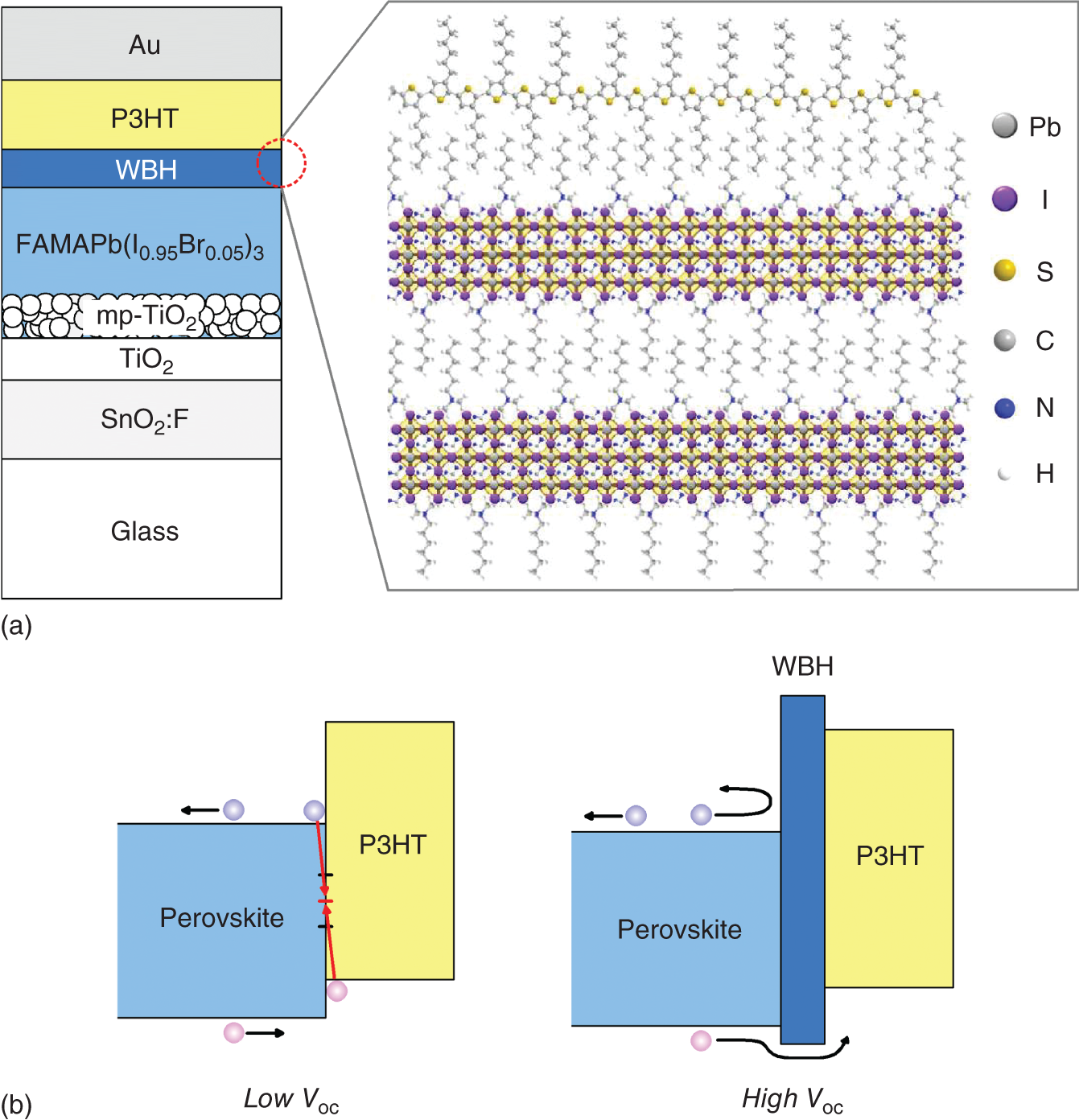
Figure 11.17 (a) Structure of a hybrid‐perovskite solar cell with a wide‐bandgap halide (WBH) passivation layer introduced at the perovskite/P3HT rear interface in an n‐i‐p cell and (b) band alignments at the perovskite/P3HT and perovskite/WBH/P3HT interfaces. In this novel structure, a thin WBH layer (12 nm), consisting of a double‐layered perovskite crystal, is formed by treating a FAMAPb(I,Br)3 absorber layer with n‐hexyl trimethlyammonium bromide (HTAB). As shown in (b), the introduction of a wide‐gap passivation layer suppresses the interface recombination, which in turn increases Voc dramatically by more than 200 mV.
Source (Atomic configuration of (a)): Jung et al. [93].
Table 11.2 summarizes the results of different passivation approaches performed for the n‐i‐p and p‐i‐n cells. The η and Voc in the table show those obtained by introducing a passivation layer (or reactant) indicated by a square bracket, whereas ΔVoc represents the Voc improvement obtained through the introduction of the passivation layer; Voc − ΔVoc in the table corresponds to the Voc of the unpassivated cells. The basic concept of passivation involves the introduction of a thin wide‐gap perovskite (a 2D planar‐type perovskite crystal) [89–93] or an insulating layer. As insulating passivation layers, various organic materials (polymers [95–101], organic salts [102–104], molecules [105, 106]), and inorganic layers (LiF [107] and Al2O3 [108]) have been adopted. In Table 11.2, the largest ΔVoc is obtained for the n‐i‐p cell shown in Figure 11.17. The passivation effect is smaller in the n‐i‐p cells with spiro‐OMeTAD HTLs (ΔVoc ∼ 50 mV). For a p‐i‐n cell, treatment of the perovskite rear surface by choline chloride [103] or guanidinium bromide [94] is particularly successful with a large ΔVoc exceeding 100 mV.
Table 11.2 Characteristics of hybrid perovskite solar cells with passivation structures.
| Cell interface structure [Passivation layer] | η (%) | Voc (V) | ΔVoc (mV) | References |
|---|---|---|---|---|
| n‐i‐p | ||||
| mp‐TiO2/FAMAPb(I,Br)3/[HTAB]a)/P3HT | 23.3 | 1.15 | 227 | [93] |
| mp‐TiO2/[PP]b)/CsFAMARbPb(I,Br)3/[PM]c)/spiro | 20.8 | 1.21 | 113 | [100] |
| mp‐TiO2/[PP]b)/CsFAMARbPb(I,Br)3/spiro | 20.4 | 1.16 | 70 | [101] |
| SnO2/FAMAPbI3/[PEAI]d)/spiro | 23.5 | 1.16 | 56 | [104] |
| mp‐TiO2/CsFAMAPb(I,Br)3/[PPI]e)/spiro | 20.7 | 1.15 | 52 | [91] |
| p‐i‐n | ||||
| PTAA/FAMAPb(I,Br)3/[CC]f)/C60 | 21.0 | 1.14 | 110 | [103] |
| PTAA/FAMAPb(I,Br)3/[GB]g)/PCBM | 21.5 | 1.21 | 100 | [94] |
| PTAA/CsFAMAPb(I,Br)3/[LiF]/C60 | 21.6 | 1.15 | 35 | [107] |
| PTAA/MAPbI3/[PS]h)/C60 | 20.3 | 1.10 | 30 | [95] |
| PTAA/MAPbI3/[BPI]i)/PCBM | 19.5 | 1.11 | 30 | [89] |
The passivation layers (or reactants) incorporated into n‐i‐p and p‐i‐n type cells are indicated by square brackets. The conversion efficiency (η) and Voc of the cells with passivation layers are summarized. The ΔVoc in the table indicates the improvement in Voc obtained by incorporating the passivation layer. Thus, Voc − ΔVoc corresponds to the Voc obtained without the passivation layer. The results are shown in descending order of ΔVoc.
a Double perovskite layer shown in Figure 11.17, formed by the reaction with n‐hexyl trimethyl ammonium bromide (HTAB).
b Layer formed by mixing poly(methyl methacrylate) (PMMA) with PCBM.
c PMMA: poly(methyl methacrylate).
d PEAI: phenethylammonium iodide.
e 2D perovskite layer in the form of PEA2PbI4 (PPI); PEA is phenylethylammonium.
f CC: choline chloride.
g Widegap layer formed by the reaction with guanidinium bromide (GB).
h PS: polystyrene.
i 2D perovskite layer in the form of (BA)2PbI4 (BPI), formed by the reaction with n‐butylamine (BA).
The results of Table 11.2 demonstrate that the passivation of the perovskite rear surface is a very important approach for achieving high Voc. Note, however, that very high Voc values of 1.23–1.26 V have been reported for the n‐i‐p and p‐i‐n cells without the introduction of passivation layers [10, 72]. Accordingly, detailed processing is also of critical importance in improving an absolute Voc. In fact, the Voc increases largely by adopting a process that enhances the ordering of PCBM molecules [109] or by minimizing the HTL doping concentration [72]. Nevertheless, the incorporation of a passivation layer is an effective approach for fabricating higher efficiency cells, enabling more effective control of the nonradiative recombination occurring at the interfaces. Moreover, the introduction of a passivation layer leads to the significant improvements in fill factor (FF), cell stability, and a reduction in unfavorable J–V hysteresis characteristics [89, 91, 93]. A state‐of‐the‐art passivation technique has also been incorporated in the fabrication of a FAPbI3‐based perovskite cell that shows a high efficiency of 24.66% [6].
11.5.3 Effect of Grain Boundary
In general, the grain boundary formation is detrimental for solar cells and the Voc of Si solar cells, for example, increases as grain size becomes larger [110]. Remarkably, even though the grain sizes of hybrid perovskite polycrystals are relatively small (∼1 μm), a very high carrier lifetime (∼8 μs) [78] and a quite high Voc [10] have been observed. Thus, nonradiative recombination at grain boundaries is suppressed extremely well in hybrid perovskite thin films. This is a characteristic that can be considered as a key factor in achieving >20% efficiencies in polycrystalline devices. In fact, efficient carrier extraction in the grain boundary region has been confirmed experimentally (Chapter 9).
Figure 11.18 shows the influence of average grain size on Voc, FF, and the diode factor n in hybrid perovskite cells with η ∼ 20% [6–8, 91, 94, 104, 111]. The n values in Figure 11.18 are extracted from the reported J–V characteristics by applying Eq. (11.3). Although data shown in Figure 11.18 are obtained from different perovskite materials and structures, the implications of the results are quite clear; (i) Voc is essentially independent of the grain size and remains unchanged unless the grain size is very small (∼100 nm) [111, 112] and (ii) FF improves markedly as the perovskite grain size increases, reaching 86% in a large‐grain MAPbI3 cell reported in Ref. [8]. The constant Voc observed at different grain sizes indicates that Voc is limited by the surface (interface) recombination and the grain boundary plays a minor role for nonradiative recombination. For the increase of FF with grain size, the improvement of n is mainly responsible and we observe n = 1.46 at large grain sizes. The results of Figure 11.18 demonstrate that perovskite polycrystals with larger grains are preferable for improving the cell efficiency.
It should be emphasized that the grain boundary significantly hinders the carrier transport in the perovskite thin films. Indeed, in‐plane carrier mobility [∼5 cm2/(V s)] is much lower than the intragrain mobility [∼30 cm2/(V s)] (see Figure 6.4). However, when the grain size exceeds the film thickness, there is no grain boundary in the carrier transport direction (i.e. vertical direction) of the cells [111] and thus the detrimental effect of the grain boundary is minimized.
For the exact grain‐boundary structures of the perovskite films, however, controversial results have been reported [11, 94, 113]. In an early report [113], it was suggested that the grain boundary is predominantly composed of PbI2 and that the perovskite grains are surrounded by thin PbI2 shells. The perovskite growth under a PbI2‐rich condition is often considered to be beneficial to enhance the grain‐boundary passivation through the PbI2 component. Nevertheless, more recent studies have shown that an excess PbI2 component is present as isolated PbI2 grains and does not exist selectively in the grain boundary region [11, 94]. To date, several attempts have been made for “grain‐boundary engineering,” in which the grain‐boundary chemical structures are modified, and the improved solar cell efficiency has been attained (see Chapter 9).

Figure 11.18 Influence of average grain size on Voc, FF, and n in various hybrid perovskite solar cells. Results obtained from different perovskite materials and structures with η ∼ 20% are summarized. The n values in the figure have been extracted by analyzing the reported J–V curves using Eq. (11.3). The average size of hybrid perovskite grains was obtained from descriptions or analyses of reported SEM images, which produce average grain sizes of <350 nm [111], 420 nm [91], 500 nm [94], 650 nm [7], 770 nm [104], 1000 nm [6], and 1500 nm [8].
Source: Min et al. [6]; Jeon et al. [7]; Chiang and Wu [8]; Cho et al. [91]; Luo et al. [94]; Jiang et al. [104]; Correa‐Baena et al. [111].
For the p‐i‐n cells with PCBM ETLs, it has been proposed that PCBM molecules diffuse from the ETL back interface into the perovskite absorber through the grain boundary region, which in turn passivates the grain‐boundary trap states [30]. As discussed above, however, the perovskite/PCBM interface shows relatively strong interface recombination and the diffusion of disordered PCBM molecules is expected to enhance the nonradiative recombination by widening the n‐type interface region. In fact, when a chemical barrier layer (i.e. passivation layer) is placed at the perovskite/PCBM (or C60) interface, Voc improves effectively (see Table 11.2). Thus, the beneficial role of PCBM diffusion into the grain boundary region is questionable.
References
- 1 Correa‐Baena, J.‐P., Saliba, M., Buonassisi, T. et al. (2017). Science 358: 739.
- 2 Jena, A.K., Kulkarni, A., and Miyasaka, T. (2019). Chem. Rev. 119: 3036.
- 3 Yang, W.S., Park, B.‐W., Jung, E.H. et al. (2017). Science 356: 1376.
- 4 Saliba, M., Correa‐Baena, J.‐P., Wolff, C.M. et al. (2018). Chem. Mater. 30: 4193.
- 5 Shin, S.S., Yeom, E.J., Yang, W.S. et al. (2017). Science 356: 167.
- 6 Min, H., Kim, M., Lee, S.‐U. et al. (2019). Science 366: 749.
- 7 Jeon, N.J., Na, H., Jung, E.H. et al. (2018). Nat. Energy 3: 682.
- 8 Chiang, C.‐H. and Wu, C.‐G. (2018). ACS Nano 12: 10355.
- 9 Saliba, M., Matsui, T., Domanski, K. et al. (2016). Science 354: 206.
- 10 Liu, Z., Krückemeier, L., Krogmeier, B. et al. (2019). ACS Energy Lett. 4: 110.
- 11 Jiang, Q., Chu, Z., Wang, P. et al. (2017). Adv. Mater. 29: 1703852.
- 12 Saliba, M., Matsui, T., Seo, J.‐Y. et al. (2016). Energy Environ. Sci. 9: 1989.
- 13 Matsui, T., Yamamoto, T., Nishihara, T. et al. (2019). Adv. Mater. 31: 1806823.
- 14 Luque, A. and Hegedus, S. (2011). Handbook of Photovoltaic Science and Engineering. West Sussex: Wiley.
- 15 Nakane, A., Fujimoto, S., and Fujiwara, H. (2017). J. Appl. Phys. 122: 203101.
- 16 Kato, Y., Fujimoto, S., Kozawa, M., and Fujiwara, H. (2019). Phys. Rev. Appl. 12: 024039.
- 17 Hara, T., Maekawa, T., Minoura, S. et al. (2014). Phys. Rev. Appl. 2: 034012.
- 18 National Renewable Energy Laboratory (2020). Best Research‐Cell Efficiencies. http://www.nrel.gov/pv/assets/pdfs/best-research-cell-efficiencies.20200406.pdf (accessed 01 April 2021).
- 19 Green, M.A., Dunlop, E.D., Hohl‐Ebinger, J. et al. (2020). Prog. Photovoltaics Res. Appl. 28: 629.
- 20 Yoshikawa, K., Kawasaki, H., Yoshida, W. et al. (2017). Nat. Energy 2: 17032.
- 21 Correa‐Baena, J.‐P., Steier, L., Tress, W. et al. (2015). Energy Environ. Sci. 8: 2928.
- 22 Wang, Q., Shao, Y., Xie, H. et al. (2014). Appl. Phys. Lett. 105: 163508.
- 23 Emara, J., Schnier, T., Pourdavoud, N. et al. (2016). Adv. Mater. 28: 553.
- 24 Cai, M., Ishida, N., Li, X. et al. (2018). Joule 2: 296.
- 25 Jacobsson, T.J., Correa‐Baena, J.‐P., Anaraki, E.H. et al. (2016). J. Am. Chem. Soc. 138: 10331.
- 26 Docampo, P., Guldin, S., Stefik, M. et al. (2010). Adv. Funct. Mater. 20: 1787.
- 27 Lin, J., Heo, Y.‐U., Nattestad, A. et al. (2015). Sci. Rep. 4: 5769.
- 28 Shirayama, M., Kadowaki, H., Miyadera, T. et al. (2016). Phys. Rev. Appl. 5: 014012.
- 29 Fujiwara, H. and Collins, R.W. (2008). Spectroscopic Ellipsometry for Photovoltaics: Applications and Optical Data of Solar Cell Materials, vol. 2. Cham: Springer‐Verlag.
- 30 Shao, Y., Xiao, Z., Bi, C. et al. (2014). Nat. Commun. 5: 5784.
- 31 Kojima, A., Teshima, K., Shirai, Y., and Miyasaka, T. (2009). J. Am. Chem. Soc. 131: 6050.
- 32 Lee, M.M., Teuscher, J., Miyasaka, T. et al. (2012). Science 338: 643.
- 33 Kim, H.‐S., Lee, C.‐R., Im, J.‐H. et al. (2012). Sci. Rep. 2: 591.
- 34 Burschka, J., Pellet, N., Moon, S.‐J. et al. (2013). Nature 499: 316.
- 35 Noh, J.H., Im, S.H., Heo, J.H. et al. (2013). Nano Lett. 13: 1764.
- 36 Heo, J.H., Im, S.H., Noh, J.H. et al. (2013). Nat. Photonics 7: 486.
- 37 Liu, M., Johnston, M.B., and Snaith, H.J. (2013). Nature 501: 395.
- 38 You, J., Meng, L., Song, T.‐B. et al. (2016). Nat. Nanotechnol. 11: 75.
- 39 Aydin, E., De Bastiani, M., and De Wolf, S. (2019). Adv. Mater. 31: 1900428.
- 40 Stolterfoht, M., Caprioglio, P., Wolff, C.M. et al. (2019). Energy Environ. Sci. 12: 2778.
- 41 Kegelmann, L., Wolff, C.M., Awino, C. et al. (2017). ACS Appl. Mater. Interfaces 9: 17245.
- 42 Chueh, C.‐C., Li, C.‐Z., and Jen, A.K.‐Y. (2015). Energy Environ. Sci. 8: 1160.
- 43 Green, M.A., Ho‐Baillie, A., and Snaith, H.J. (2014). Nat. Photonics 8: 506.
- 44 Schulz, P., Edri, E., Kirmayer, S. et al. (2014). Energy Environ. Sci. 7: 1377.
- 45 Olthof, S. (2016). APL Mater. 4: 091502.
- 46 Tao, S., Schmidt, I., Brocks, G. et al. (2019). Nat. Commun. 10: 2560.
- 47 Burgelman, M., Nollet, P., and Degrave, S. (2000). Thin Solid Films 361–362: 527.
- 48 Diekmann, J., Caprioglio, P., Rothhardt, D. et al. (2019). arXiv: 1910.07422.
- 49 Mandadapu, U., Vedanayakam, S.V., Thyagarajan, K. et al. (2017). Int. J. Renew. Energy Res. 7: 1603.
- 50 Tan, K., Lin, P., Wang, G. et al. (2016). Solid State Electron. 126: 75.
- 51 Tress, W., Marinova, N., Inganäs, O. et al. (2014). Adv. Energy Mater. 5: 1400812.
- 52 Tvingstedt, K., Malinkiewicz, O., Baumann, A. et al. (2014). Sci. Rep. 4: 6071.
- 53 Fujiwara, H., Kato, M., Tamakoshi, M. et al. (2018). Phys. Status Solidi A 215: 1700730.
- 54 Nakane, A., Tampo, H., Tamakoshi, M. et al. (2016). J. Appl. Phys. 120: 064505.
- 55 Edri, E., Kirmayer, S., Henning, A. et al. (2014). Nano Lett. 14: 1000.
- 56 Edri, E., Kirmayer, S., Mukhopadhyay, S. et al. (2014). Nat. Commun. 5: 3461.
- 57 Jiang, C.‐S., Yang, M., Zhou, Y. et al. (2015). Nat. Commun. 6: 8397.
- 58 Guerrero, A., Juarez‐Perez, E.J., Bisquert, J. et al. (2014). Appl. Phys. Lett. 105: 133902.
- 59 Bergmann, V.W., Weber, S.A.L., Ramos, F.J. et al. (2014). Nat. Commun. 5: 5001.
- 60 Fujiwara, H. and Collins, R.W. (2018). Spectroscopic Ellipsometry for Photovoltaics: Fundamental Principles and Solar Cell Characterization, vol. 1. Cham: Springer.
- 61 Fujiwara, H. and Kondo, M. (2005). Phys. Rev. B 71: 075109.
- 62 Bhachu, D., Waugh, M.R., Zeissler, K. et al. (2011). Chem. Eur. J. 17: 11613.
- 63 This software can be downloaded at the web site of https://unit.aist.go.jp/rpd-envene/PV/en/service/e-ARC_en/index_en.html. This web site can be found using “e‐ARC AIST” as key words (accessed 01 April 2021).
- 64 Tavakoli, M.M., Tress, W., Milić, J.V. et al. (2018). Energy Environ. Sci. 11: 3310.
- 65 Shi, J., Dong, J., Lv, S. et al. (2014). Appl. Phys. Lett. 104: 063901.
- 66 Etgar, L., Gao, P., Xue, Z. et al. (2012). J. Am. Chem. Soc. 134: 17396.
- 67 Ogomi, Y., Morita, A., Tsukamoto, S. et al. (2014). J. Phys. Chem. Lett. 5: 1004.
- 68 Zhao, B., Abdi‐Jalebi, M., Tabachnyk, M. et al. (2017). Adv. Mater. 29: 1604744.
- 69 Sze, S.M. (1981). Physics of Semiconductor Devices. New York: Wiley‐Interscience.
- 70 Shockley, W. and Queisser, H.J. (1961). J. Appl. Phys. 32: 510.
- 71 Liu, F., Dong, Q., Wong, M.K. et al. (2016). Adv. Energy Mater. 6: 1502206.
- 72 Correa‐Baena, J.‐P., Tress, W., Domanski, K. et al. (2017). Energy Environ. Sci. 10: 1207.
- 73 Eperon, G.E., Burlakov, V.M., Docampo, P. et al. (2014). Adv. Funct. Mater. 24: 151.
- 74 Wang, Y., Dar, M.I., Ono, L.K. et al. (2019). Science 365: 591.
- 75 Shen, D., Yu, X., Cai, X. et al. (2014). J. Mater. Chem. A 2: 20454.
- 76 Zhang, H., Cheng, J., Lin, F. et al. (2016). ACS Nano 10: 1503.
- 77 Tan, H., Che, F., Wei, M. et al. (2018). Nat. Commun. 9: 3100.
- 78 deQuilettes, D.W., Koch, S., Burke, S. et al. (2016). ACS Energy Lett. 1: 438.
- 79 Braly, I.L., deQuilettes, D.W., Pazos‐Outón, L.M. et al. (2018). Nat. Photonics 12: 355.
- 80 Yang, Y., Yang, M., Moore, D.T. et al. (2017). Nat. Energy 2: 16207.
- 81 Sarritzu, V., Sestu, N., Marongiu, D. et al. (2017). Sci. Rep. 7: 44629.
- 82 Wolff, C.M., Caprioglio, P., Stolterfoht, M., and Neher, D. (2019). Adv. Mater. 31: 1902762.
- 83 Rau, U. (2007). Phys. Rev. B 76: 085303.
- 84 Vandewal, K., Tvingstedt, K., Gadisa, A. et al. (2009). Nat. Mater. 8: 904.
- 85 Yao, J., Kirchartz, T., Vezie, M.S. et al. (2015). Phys. Rev. Appl. 4: 014020.
- 86 Xing, G., Mathews, N., Sun, S. et al. (2013). Science 342: 344.
- 87 Stranks, S.D., Eperon, G.E., Grancini, G. et al. (2013). Science 342: 341.
- 88 Hutter, E.M., Eperon, G.E., Stranks, S.D., and Savenije, T.J. (2015). J. Phys. Chem. Lett. 6: 3082.
- 89 Lin, Y., Bai, Y., Fang, Y. et al. (2018). J. Phys. Chem. Lett. 9: 654.
- 90 Chen, P., Bai, Y., Wang, S. et al. (2018). Adv. Funct. Mater. 28: 1706923.
- 91 Cho, K.T., Grancini, G., Lee, Y. et al. (2018). Energy Environ. Sci. 11: 952.
- 92 Cho, Y., Soufiani, A.M., Yun, J.S. et al. (2018). Adv. Energy Mater. 8: 1703392.
- 93 Jung, E.H., Jeon, N.J., Park, E.Y. et al. (2019). Nature 567: 511.
- 94 Luo, D., Yang, W., Wang, Z. et al. (2018). Science 360: 1442.
- 95 Wang, Q., Dong, Q., Li, T. et al. (2016). Adv. Mater. 28: 6734.
- 96 Wolff, C.M., Zu, F., Paulke, A. et al. (2017). Adv. Mater. 29: 1700159.
- 97 Chaudhary, B., Kulkarni, A., Jena, A.K. et al. (2017). ChemSusChem 10: 2473.
- 98 Wang, F., Shimazaki, A., Yang, F. et al. (2017). J. Phys. Chem. C 121: 1562.
- 99 Zuo, L., Guo, H., deQuilettes, D.W. et al. (2017). Sci. Adv. 3: e1700106.
- 100 Peng, J., Khan, J.I., Liu, W. et al. (2018). Adv. Energy Mater. 8: 1801208.
- 101 Peng, J., Wu, Y., Ye, W. et al. (2017). Energy Environ. Sci. 10: 1792.
- 102 Zhao, T., Chueh, C.‐C., Chen, Q. et al. (2016). ACS Energy Lett. 1: 757.
- 103 Zheng, X., Chen, B., Dai, J. et al. (2017). Nat. Energy 2: 17102.
- 104 Jiang, Q., Zhao, Y., Zhang, X. et al. (2019). Nat. Photonics 13: 460.
- 105 Wang, F., Geng, W., Zhou, Y. et al. (2016). Adv. Mater. 28: 9986.
- 106 Lin, Y., Shen, L., Dai, J. et al. (2017). Adv. Mater. 29: 1604545.
- 107 Stolterfoht, M., Wolff, C.M., Márquez, J.A. et al. (2018). Nat. Energy 3: 847.
- 108 Koushik, D., Verhees, W.J.H., Kuang, Y. et al. (2017). Energy Environ. Sci. 10: 91.
- 109 Shao, Y., Yuan, Y., and Huang, J. (2016). Nat. Energy 1: 15001.
- 110 Werner, J.H., Dassow, R., Rinke, T.J. et al. (2001). Thin Solid Films 383: 95.
- 111 Correa‐Baena, J.‐P., Anaya, M., Lozano, G. et al. (2016). Adv. Mater. 28: 5031.
- 112 Saliba, M., Correa‐Baena, J.‐P., Grätzel, M. et al. (2018). Angew. Chem. Int. Ed. 57: 2554.
- 113 Chen, Q., Zhou, H., Song, T.‐B. et al. (2014). Nano Lett. 14: 4158.