12
Efficiency Limits of Single and Tandem Solar Cells
Hiroyuki Fujiwara1, Yoshitsune Kato1, Masayuki Kozawa1, Akira Terakawa2 and Taisuke Matsui3
1Gifu University, Department of Electrical, Electronic and Computer Engineering, 1‐1 Yanagido, Gifu, 501‐1193, Japan
2Panasonic Corporation, Energy System Division, 15‐2 Nishikiminamimachi, Kaizuka, Osaka, 597‐0094, Japan
3Panasonic Corporation, Technology Innovation Division, 3‐1‐1 Yagumo‐naka‐machi, Moriguchi City, Osaka, 570‐8501, Japan
12.1 Introduction
The theoretical interpretation of solar‐cell performances is critical, as it reveals the efficiency‐limiting factors of experimental photovoltaic devices [1]. Based on the physics of solar cells, the maximum possible parameters for short‐circuit current density (Jsc), open‐circuit voltage (Voc), and fill factor (FF), as well as the resulting conversion efficiency (η), can be estimated individually [1, 2]. The best‐known approach for calculating the solar‐cell efficiency limit is that developed by Shockley and Queisser more than half a century ago [2]. Since then, the Shockley–Queisser (SQ) limit has been adopted extensively as an absolute criterion that sets the maximum possible limit of solar‐cell efficiency. Remarkably, the SQ limit is estimated by considering only a single physical quantity: the band gap (Eg) of a light absorber at room temperature. Figure 12.1 shows the variation of the SQ limit with Eg, together with the conversion efficiencies of experimental record‐efficiency cells [3–7], including methylammonium lead iodide (CH3NH3PbI3; MAPbI3) [4] and formamidinium lead iodide [HC(NH2)2PbI3; FAPbI3] [5] solar cells. The numerical values of the SQ limit are summarized in Appendix B. It can be seen from Figure 12.1 that the SQ limit exhibits high efficiencies of η ∼ 33% in a broad Eg range of 1.1–1.4 eV.
The conversion efficiencies derived from SQ theory are, however, substantially higher than those of the most efficient experimental cells developed to date. In particular, even for the most ideal GaAs cell, the experimental efficiency (η = 29.1% [3]) is substantially inferior to the maximum SQ efficiency of 33.7%. This is, in part, attributed to the overestimated efficiency limit under the SQ model, which is based on highly idealized physical assumptions that can never be achieved in the real world. For example, the theory assumes an infinitely thick light absorber with absolutely zero light reflection (i.e. a perfect light absorber).

Figure 12.1 Maximum efficiency (η) for different Eg derived from SQ theory (solid line), together with the conversion efficiencies of experimental world record‐efficiency cells reported in Refs. [3–7] (circles), including CuInGaSe2 (CIGSe), Cu2ZnSn(S,Se)4 (CZTSSe), and hydrogenated amorphous silicon (a‐Si:H). The efficiencies of the experimental FAPbI3 and MAPbI3 cells are η = 24.66% [5] and 21.3% [4], respectively. For the FAPbI3 cell, a small amount of methylenediammonium dichloride (MDACl2) is incorporated. The numerical values corresponding to the SQ limit are summarized in Appendix B.
Source: Green et al. [3]; Shin et al. [4]; Min et al. [5]; Green et al. [6]; Lee et al. [7].
A more rigorous approach has been developed to more accurately determine the absolute physical limits of thin‐film solar cells, enabling a better understanding of the performance limits of experimental cells [1]. This approach can further be extended to interpret and simulate the performance of perovskite tandem devices. As the tandem solar‐cell architecture is complex [8–11], an accurate simulation is of significant importance in designing and improving such devices.
In this chapter, we review all fundamental aspects that are necessary for understanding the theoretical estimation of single‐ and tandem‐cell efficiency limits. We begin by presenting the basic principles of SQ theory (Section 12.2), introducing the optical/physical models adopted in the SQ limit calculation. The latest approach for realistic maximum‐efficiency calculation, which has been developed for solar cells in conventional thin‐film forms, is explained in Section 12.3. Finally, a rigorous estimation of tandem‐cell efficiency is presented in Section 12.4.
12.2 What Is the SQ Limit?
In 1961, Shockley and Queisser developed a theory for predicting the ultimate limit of solar‐cell efficiency [2]. This SQ model is based on a simple and straightforward assumption that each photon generates a single electron–hole pair in a p–n junction solar cell at thermal equilibrium. Nevertheless, the understanding of SQ theory is slightly difficult as this model includes a unique physical concept of blackbody radiation. This section provides a step‐by‐step introduction to SQ theory, which forms a basis for calculating the maximum solar‐cell efficiency. Specifically, the physical model assumed in the SQ approach is explained in Section 12.2.1 and the physics of blackbody radiation is fully described in Section 12.2.2. Based on these explanations, the principle of SQ theory (Section 12.2.3) can be understood rather easily.
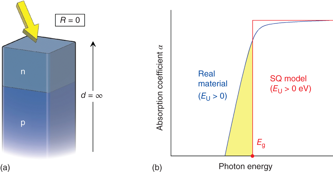
Figure 12.2 (a) Optical model assumed for Shockley–Queisser (SQ) theory and (b) absorption coefficient (α) spectra of the SQ model and a real material. In the SQ model, a p–n homojunction cell with infinite thickness is assumed while forcing the reflectance R of this hypothetical structure to zero (i.e. R = 0). For the SQ model, a step‐function α spectrum is applied; in contrast, a real material shows finite‐tail absorption with nonzero Urbach energy (i.e. EU > 0).
12.2.1 Physical Model
The solar‐cell structure assumed under SQ theory is simple (Figure 12.2a). In this model, a p–n homojunction cell with an infinite thickness is assumed while forcing the reflectance R of this hypothetical structure to zero (i.e. R = 0). Figure 12.2b schematically shows the absorption coefficient (α) spectra for the SQ model and a conventional material. Under SQ theory, the α spectrum of the absorber is modeled as a simple step function that shows infinite absorption at the photon energy of E ≥ Eg. Note that the experimental materials exhibit tail absorption below Eg with Urbach energies of EU > 0 (see Figure 4.17); in contrast, EU = 0 is assumed for SQ theory.
In SQ theory, the current density–voltage (J–V) characteristic is modeled by the following simple diode equation [12, 13]:

where J0 is the reverse saturation current density (i.e. dark current) and q, kB, and T are the electron charge, Boltzmann constant, and temperature, respectively. In Eq. (12.1), there are only two critical variables (i.e. Jsc and J0) and the solar‐cell parameters Voc, FF, and η can be calculated from the J–V curve based on (Jsc, J0). In the SQ limit, Jsc is simply estimated by assuming that all electron–hole pairs generated by a 1‐sun illumination (ϕ1Sun) are collected in the energy region E ≥ Eg. Compared to this simple photocurrent calculation, the estimation of the dark current (J0) is more complex.
Figure 12.3 shows a physical representation of the SQ model, which is considered for the J0 calculation. In this approach, a p–n homojunction solar cell is placed in a cavity surrounded by a spherical blackbody held at 300 K. A blackbody is a hypothetical object that absorbs all incoming light, regardless of the wavelength and angle of incidence (i.e. R = 0). At elevated temperatures, the blackbody emits electromagnetic waves, which are known as the blackbody radiation. For example, even though graphite is almost completely black, it emits a wide spectrum of blackbody radiation when heated. In the SQ model, the p–n cell is treated as a perfect blackbody in the energy region above Eg, while it is completely transparent at E < Eg.

Figure 12.3 Physical model of the SQ model adopted for J0 calculation. In the SQ model, a p–n homojunction solar cell is surrounded by a spherical blackbody held at 300 K. The absorption of blackbody photons leads to the carrier generation with a current flow of J0 in the cell. The carrier generation by photon absorption is in equilibrium with the radiative carrier recombination.
In Figure 12.3, the p–n cell and a spherical blackbody radiator are in thermal equilibrium. If the spherical blackbody radiator is held at 300 K, it emits photons with energies corresponding to those of infrared light (see Section 12.2.2). The generated blackbody photons are absorbed by the solar cell, creating the electron–hole pairs within the absorber. Note that the solar cell in the figure is under the dark condition because it is surrounded completely by the spherical blackbody. In a room covered completely by a thick graphite at 300 K, human eyes cannot detect any light, but blackbody radiation still occurs, generating the dark current in solar cells.
As illustrated in Figure 12.3, the photon absorption in the cell generates carriers with a current flow of J0. If the direction of the J0 current is reversed, radiative recombination of carriers occurs, leading to photon radiation (emission). The key assumption of the SQ model is that the rate of photon absorption is exactly equal to the rate of photon emission; therefore, within the cavity, a detailed balance is maintained by the photon exchange, resulting in a complete thermal equilibrium of the system. In other words, in this model, J0 is ultimately considered as a “virtual current” at V = 0, where the current flow generated by photon absorption is counterbalanced by the reverse current flow due to radiative recombination with a net current being J = 0. Consequently, under the SQ approach, J0 is estimated from the absorption of blackbody photons at 300 K. By applying the (Jsc, J0) values obtained from the above‐described procedures, the J–V characteristics of a maximum‐efficiency cell can be evaluated using Eq. (12.1). This is the fundamental physics of SQ theory.
12.2.2 Blackbody Radiation
Blackbody radiation is governed by a single physical parameter – temperature T. As the physical model of blackbody radiation forms the core of solar‐cell limit calculations, the derivation of the Planck's law (http://www.ioa.s.u-tokyo.ac.jp/kisohp/STAFF/nakada/Jugyo/G=Blackbody.ppt) is explained fully in this section.
For this purpose, we consider a blackbody cube with equal sides of length L (i.e. the volume is V = L3). The interior of the cube is empty, but the space inside the cube is filled with blackbody radiation, which is under thermal equilibrium with the blackbody wall maintained at T. The blackbody radiation for a wavelength of λ at T is denoted by γBB(λ, T). To describe γBB, a wavelength space for the photons within the unit volume is defined (Figure 12.4a). This wavelength space differs from the real space and is defined by two factors: λ and the moving direction of the photon (Ω). The dΩ indicates the solid angle for a traveling photon and the area of the basal plane is A = λ2 dΩ. When the frustum formed by dλ is considered, its volume becomes λ2 dλ dΩ. If a photon number density of ρn is applied, the number of photons in the frustum is given as p = ρnλ2 dλ dΩ per unit volume. In the corresponding real space (Figure 12.4b), on the other hand, the number of photons passing through the small area dS during the time interval dt is expressed as v = c dt dS, where c is the speed of light. Accordingly, the photon number (dN) can be calculated as the product of the real‐space volume (v = c dt dS) and the number of photons per unit volume in the wavelength space (i.e. p calculated above):

Figure 12.4 Definitions of blackbody radiation in (a) the wavelength space for photons in the unit volume and (b) the real space. The moving direction of photon is Ω, whereas dΩ indicates the solid angle covered by the path of a traveling photon. In (a), A is the area of the basal plane. The c in (b) shows the speed of light.
Because the energy of a single photon is given by E = hc/λ (Einstein relation), the energy transferred by dN is dE = (hc/λ)dN. Thus,
where
To derive ρn, we consider the quantum state within the cube (V = L3). For a photon to exist stably within the cube, its wavelength λ in the x, y, and z directions must be exactly the same as L and thus the number of the photon states per volume V is given by

Here, the factor of 2 indicates that the electromagnetic wave can be in two states with different polarizations. By setting ΔVλ = ΔλxΔλyΔλz in Eq. 12.5, we can estimate the density of the quantum state as ρQ = ΔU/ΔVλ = 2/λ6. On the other hand, the quantum‐mechanical consideration provides the occupation number of photons in the quantum state of λ as follows (http://www.ioa.s.u-tokyo.ac.jp/kisohp/STAFF/nakada/Jugyo/G=Blackbody.ppt):
As a result, ρn is derived as ρn = ρQΘ and thus γBB of Eq. 12.4 becomes
If hemispherical integration is considered for the blackbody radiation in Figure 12.3, γBB is multiplied by π (see Section 12.2.3). In this case, the density of blackbody photons (ϕBB) per second per meter square can be estimated by dividing γBB by E(=hc/λ):

Often, a value of ϕBB derived for the photon energy is employed (i.e. ϕBB(E, T)). From Eq. (12.3), γBB(E, T) = γBB(λ, T)|dλ/dE|. Since |dλ/dE| = hc/E2, we obtain

Figure 12.5a shows the variation of ϕBB(E, T) with T, calculated from Eq. (12.9). The spectrum of blackbody photon density changes drastically with T and extends toward the ultraviolet region (E ∼ 3 eV) as T increases. At 300 K, the ϕBB spectrum is nonuniform and ϕBB increases in the infrared region (E ∼ 1 eV); thus, J0 increases significantly when Eg becomes lower. The spectrum of sunlight can be approximated by setting T = 6000 K. In Figure 12.5b, the photon density produced by 1‐sun illumination (ϕ1Sun) under the AM1.5G condition is compared with the blackbody radiation density at T = 6000 K and a close match is observed.

Figure 12.5 (a) Variation in blackbody photon density ϕBB(E, T) with T, calculated from Eq. (12.9) and (b) photon density of 1‐sun illumination (ϕ1Sun) under the AM1.5G condition, which is compared with blackbody radiation density at T = 6000 K.
12.2.3 SQ Limit
Once the fundamental blackbody concept discussed in Section 12.2.2 is understood, the SQ theoretical‐limit calculation becomes straightforward. Figure 12.6a shows the general procedure established under SQ theory for calculating the maximum efficiency. In this method, the optical model is first defined and then used to calculate the external quantum efficiency (EQE). Once the EQE spectrum is known, Jsc and J0 can be calculated from ϕ1Sun (Figure 12.5b) and ϕBB (Figure 12.5a at T = 300 K), respectively, as described below. Based on (Jsc, J0), the J–V curve can be calculated from Eq. (12.1), from which all the other solar‐cell parameters (i.e. Voc, FF, and η) are deduced.

Figure 12.6 (a) Procedure of maximum‐efficiency calculation and (b) example of J0 estimation with Eg = 1.4 eV under SQ theory. Here, J0 is calculated as the product of EQE and ϕBB (see Eq. 12.12). The ϕBB spectrum in (b) is consistent with that shown in Figure 12.5a.
Figure 12.6b shows an example of estimating J0 at Eg = 1.4 eV under SQ theory. In the SQ model, (i) an infinite absorber thickness, (ii) a step‐function α, and (iii) R = 0 are assumed, which lead to the step‐function EQE spectrum of QSQ = 1 (E ≥ Eg) and QSQ = 0 (E < Eg). Under SQ theory, J0 is essentially calculated as an overlap between EQE and ϕBB at 300 K (see Figure 12.6b). Accordingly, J0 increases drastically as Eg decreases.
The actual calculation of J0 is conducted by considering a hemispherical configuration (Figure 12.7a), in which the blackbody radiation onto a p–n junction solar cell is integrated over a series of solid angles θ and rotation angles φ. We consider the blackbody radiation emitted from a small ring‐like area, defined by dθ (gray area in Figure 12.7a). For a hemisphere of radius r, the total gray area on the hemisphere is dS = 2πrsin θL, where L is the latitudinal distance L = r dθ. We further consider the projection of the area dS onto a p–n junction surface with the area of dS′ (Figure 12.7b). When the radiation from dS is projected onto dS′ at an incident angle of θ, we find a simple relation dS′ = cos θ dS.
The total number of blackbody photons entering the p–n solar cell through the area dS′ is expressed as
where the prefactor of λ/hc(=1/E) corresponds to the conversion of radiation into photon density, as explained in Eq. (12.8). If r = 1, we obtain dS′ = 2πsin θ cos θ dθ, which can be substituted into Eq. 12.10 to obtain
In the above equation, θ is integrated over the range 0°–90° and the relation of ![]() is used. As
is used. As ![]() , the spherical integrations of dθ and dφ produce a value of π (i.e. 2π ⋅ 1/2) and ϕBB(λ) in Eq.
12.11 is reduced to that in Eq.
12.8. Finally, ϕBB(λ) can be integrated over λ to estimate J0:
, the spherical integrations of dθ and dφ produce a value of π (i.e. 2π ⋅ 1/2) and ϕBB(λ) in Eq.
12.11 is reduced to that in Eq.
12.8. Finally, ϕBB(λ) can be integrated over λ to estimate J0:

Figure 12.7 (a) Integration method used for the J0 calculation under SQ theory and (b) projection of area dS onto p–n junction surface with an area of dS′. In (a), θ and φ show solid and rotation angles, respectively, whereas r denotes the hemisphere radius. The gray area (dS) indicates the area defined by the variation in dθ.
as illustrated in Figure 12.6b. Under SQ theory, a perfect blackbody solar cell is assumed and the EQE is always unity above Eg, independent of θ and φ. On the other hand, Jsc of the cell can be calculated by assuming 100% carrier collection at normal incidence:

From the obtained (J0,SQ, Jsc,SQ), the solar‐cell parameters can be calculated based on Eq. (12.1).
Figure 12.8 shows the variation of Jsc, Voc, and FF with the absorber Eg, estimated from the above SQ approach (solid lines), together with the experimental parameters obtained from record‐efficiency solar cells (circles) reported in Refs. [3–7]. The corresponding efficiencies are shown in Figure 12.1. All SQ parameters in Figures 12.1 and 12.8 are summarized in Appendix B. The Jsc result is calculated from Eq. 12.13 using ϕ1Sun shown in Figure 12.5b and Jsc decreases as Eg becomes wider. The Voc of the SQ model is calculated directly from Voc = kB/q[ln(Jsc,SQ/J0,SQ) + 1]. Unlike Jsc, Voc increases with Eg, primarily because J0 decreases logarithmically at higher Eg (see Figure 12.6b). The dotted line shows Voc derived directly from Eg (i.e. Voc = Eg/q). The Voc obtained under SQ theory is smaller than Eg/q by 0.2–0.3 V, while FF remains essentially constant. As a result, the conversion efficiency calculated under SQ theory reaches a maximum at Eg = 1.34 eV.
![Schematic illustration of variation in Jsc, Voc, and FF with Eg of the absorber, calculated under SQ theory (solid lines), together with the experimental values of record-efficiency solar cells reported in Refs. [3-7] (circles).](https://imgdetail.ebookreading.net/2023/10/9783527347292/9783527347292__9783527347292__files__images__c12f008.png)
Figure 12.8 Variation in Jsc, Voc, and FF with Eg of the absorber, calculated under SQ theory (solid lines), together with the experimental values of record‐efficiency solar cells reported in Refs. [3–7] (circles). The corresponding efficiencies are shown in Figure 12.1. The conversion efficiencies of the experimental FAPbI3 and MAPbI3 cells are η = 24.66% [5] and 21.3% [4], respectively. For the FAPbI3 cell, a small amount of methylenediammonium dichloride (MDACl2) has been incorporated. The dotted line shows the Voc derived directly from Eg (i.e. Voc = Eg/q). The numerical values corresponding to the SQ limit are summarized in Appendix B.
In Figure 12.8, the SQ calculation result reproduces the overall experimental trends well. However, all the experimental solar cells show lower values compared with the SQ results. The reduction from the theoretical Jsc can be attributed to (i) the unfavorable light absorption occurring in transparent conductive oxide (TCO) and doped layers of the cells and (ii) the nonzero light reflection in the experimental solar cells, which is neglected completely in the SQ model. The lower Voc in the experimental cells originates from (i) the tail absorption (EU > 0), which reduces the effective Eg and Voc, and (ii) the effect of nonradiative recombination (Section 11.4.2). The reduction of FF in the experimental solar cells can be understood by finite series and shunt resistances as well as the increase in the nonideal diode factor, which is neglected in Eq. (12.1), as explained in Section 11.4.2.
12.3 Maximum Efficiencies of Perovskite Single Cells
The SQ limit is determined completely by Eg and does not reflect the optical properties of an actual absorber material. For hybrid perovskite layers fabricated by spin‐coating processes, the maximum thickness is ∼1 μm [14] and thus the infinite absorber thickness assumed in the SQ model is not valid. Furthermore, the SQ assumptions of R = 0 and no tail absorption (see Figure 12.2) cannot be realized in experimental solar cells, contributing to the overestimation of the theoretical limits. Note that R = 0 is observed only when the refractive index of the p–n diode is equal to one with no light absorption. From an optical point of view, therefore, the SQ model is highly hypothetical.
In this section, we introduce a new approach that has been developed to calculate more accurate efficiency limits, particularly in thin‐film solar cells (Section 12.3.1). In this approach, the calculation of realistic EQE spectra for thin‐film solar cells is crucial (Section 12.3.2). In Section 12.3.3, we see the maximum efficiencies of representative solar cells in a 1‐μm‐thick physical limit. Based on theoretical thin‐film limits, the performance‐limiting factors of hybrid perovskite devices are further discussed in Section 12.3.4.
12.3.1 Concept of Thin‐Film Limit
For thin‐film efficiency calculation, a rigorous approach that incorporates all physical and optical aspects of real‐world solar cell has been developed by extending SQ theory [1]. In this scheme, a theoretical efficiency limit for a perfectly realizable thin‐film structure in Figure 12.9a is estimated by adopting the true absorption characteristics of the light absorber and constituent layers. In this thin‐film concept, a general layer‐stacked structure of TCO (70 nm)/absorber (p–n layers: 1 μm)/metal (Ag) is considered. To maximize the light absorption of the thin‐film solar cell, the entire cell structure is assumed to be textured. A dual antireflection coating of MgF2/Al2O3 is further incorporated to minimize the front light reflection. In addition, a front metal‐grid electrode with a shadow loss of 5% is assumed.

Figure 12.9 (a) Optical model assumed for thin‐film limit calculation and (b) physical model of a thin‐film device placed in a cavity surrounded by a blackbody radiator. In the thin‐film limit calculation, a non‐blackbody cell (i.e. R ≠ 0) is assumed. In the model of (a), MgF2 and Al2O3 are antireflecting coating, whereas In2O3:H is a high‐mobility TCO material. The area of metal‐grid electrode (shadow loss) is assumed to be 5%.
Source: Kato et al. [1].
In a thin‐film solar cell with a limited absorber thickness, strong optical confinement is crucial for increasing Jsc. In the optical calculation of the structure shown in Figure 12.9a, all optical confinement effects due to texture, antireflection coating, and backside reflection are fully incorporated. Moreover, the light reflection of the solar cell is not assumed to be zero (R ≠ 0) and thus a non‐blackbody cell is considered. For solar cells, the presence of TCO is generally problematic because the free carriers (electrons) in the TCO exhibit strong light absorption, which reduces Jsc rather significantly [15–19]. In the thin‐film model, to suppress unfavorable parasitic absorption in the TCO, a high‐mobility TCO layer (H‐doped In2O3 [20, 21]) with a mobility of μ = 100 cm2/(V s) and a low carrier concentration of 2 × 1020 cm−3 is assumed. The use of high‐mobility TCO is particularly important in obtaining a sufficiently low TCO series resistance at low carrier concentrations [20]. The carrier concentration in commercial SnO2:F substrates (TEC substrates) is 5 × 1020 cm−3 (μ = 30 cm2/(V s)) [20, 22] and the free carrier absorption is substantially stronger. The optical constants of hybrid perovskites can be found in Appendix A and those of the constituent layers can be obtained from Refs. [1, 15].
To estimate the J0 of a solar cell with the structure of Figure 12.9a, the solar cell is placed in a spherical cavity surrounded by a blackbody radiator (Figure 12.9b). For a non‐blackbody thin‐film cell (R ≠ 0), the optical response is incident‐angle‐dependent and the optical calculation must be carried out by considering the p‐ and s‐polarized waves (see Figure 4.11a for definitions of these polarizations). Specifically, the incident‐angle‐dependent EQE spectrum (i.e. Q(λ, θ)) is estimated as a simple average of the EQE spectra calculated for the p‐polarization [Qp(λ, θ)] and s‐polarization [Qs(λ, θ)]:
In the configuration of Figure 12.9b, ϕBB(λ) in Eq. (12.10) is expressed using the θ‐dependent function ϕBB(λ, θ). Over a small area dθ dφ, we obtain ϕBB(λ) = ∫∫ϕBB(λ, θ)dθ dφ. By inserting this equation and Eq. (12.14) into Eq. (12.12), the blackbody radiation from all the internal surface of the cavity can be integrated using the following exact formula:

where S is the shadow loss of the front metal‐grid electrode (S = 0.05). On the other hand, the Jsc of the solar cell is calculated using the standard equation of

where Qθ=0(λ) is the EQE spectrum at θ = 0°. From Jsc and J0 above, the thin‐film solar‐cell limit can be obtained using Eq. (12.1).
12.3.2 EQE Calculation Method
The EQE spectra Qp(λ, θ) and Qs(λ, θ) in Eq. (12.15) can be calculated by applying the antireflection condition (ARC) approach [15–17]. This scheme allows for the incorporation of all possible optical effects generated in textured solar cells. Figure 12.10a shows an example of calculating EQE using the ARC method for a MAPbI3 absorber at θ = 0°. In the ARC method, the R spectrum is first calculated by considering a flat multilayer structure using a conventional optical admittance method [15, 16, 23]. The result obtained assuming this flat structure is indicated as Rflat in Figure 12.10a. Next, the minimum R points in the Rflat spectrum (open circles) are selected and connected linearly. In the ARC method, the resulting spectrum represents the R spectrum of a textured structure (Rtex) that incorporates the widely observed antireflection effect in random textured structures. By adopting this Rtex spectrum, the EQE spectrum of a random texture can be approximated based on the optical calculation using a flat optical model [15–17]. This simple approach has been applied successfully in reproducing the optical response of numerous submicron‐textured solar cells, including hybrid perovskite [16], CIGSe [17], CZTSSe [16], and CdTe [16]. A free Windows‐based software has been released to calculate EQE based on the ARC method (see Figure 11.13) [24].
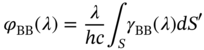
Figure 12.10b shows an ARC‐calculated EQE spectrum plotted on a logarithmic scale. In the visible region, the EQE is almost 100% but is reduced in the ultraviolet region (λ ∼ 300 nm) due to parasitic absorption by the TCO layer. The figure also shows ϕBB at 300 K, indicating the drastic increase in this factor in the longer λ region. In Figure 12.10c, the λ‐dependent J0 contribution (J0,λ) calculated from J0,λ = (1 − S)qQθ=0(λ)ϕBB(λ) is shown. Note that J0 is determined by integrating the J0,λ spectrum. The result in the figure illustrates the importance of the near‐band‐edge EQE in determining J0. In an absorber with extensive tail absorption, the EQE spectrum is extended toward the longer λ region, which in turn increases J0 and reduces Voc significantly [1].
Figure 12.10 Calculation of the EQE spectrum and J0 for a MAPbI3 absorber at an incident angle of θ = 0°: (a) reflectance spectrum, (b) EQE, and (c) λ‐dependent J0 contribution (J0,λ). The reflectance and EQE spectra are estimated by applying the ARC method [15–17] (see also Figure 11.13). The Rflat and Rtex in (a) show the reflectance spectra for flat and textured structures, respectively. The EQE spectrum in (b) is calculated based on Rtex. The J0,λ in (c) is estimated from the EQE and ϕBB in (b) as J0,λ = (1 − S)qQθ=0(λ)ϕBB(λ), where S and Qθ=0(λ) show the shadow loss and EQE spectrum at θ = 0°, respectively.
In the above example, θ = 0° is assumed and J0 is calculated as
This simple approach has been employed widely in the estimation of approximate J0 values [25–27]. Importantly, it has been confirmed that the J0 values obtained using the detailed integration of Eq. (12.15) and the simplified calculation of Eq. (12.17) fall into similar ranges (Figure 12.11) [1]. Accordingly, although an exact calculation using Eq. (12.15) is preferable, Eq. (12.17) can still be adopted to estimate an approximate value.
![Schematic illustration of {Shockley-Queisser (SQ) limit!perovskite single cells!EQE calculation methodRelationship between J0 values calculated assuming θ ≠ 0° and θ = 0° [1]. The J0 values of θ ≠ 0° were evaluated by performing an exact spherical integration of the protect structure in Figure 12.9b using Eq. (12.15), whereas the J0 values of θ = 0° were obtained using Eq. (12.17) assuming a normal incidence for the EQE calculation.](https://imgdetail.ebookreading.net/2023/10/9783527347292/9783527347292__9783527347292__files__images__c12f011.png)
Figure 12.11 Relationship between J0 values calculated assuming θ ≠ 0° and θ = 0° [1]. The J0 values of θ ≠ 0° were evaluated by performing an exact spherical integration of the structure in Figure 12.9b using Eq. 12.15, whereas the J0 values of θ = 0° were obtained using Eq. 12.17 assuming a normal incidence for the EQE calculation.
Source: Kato et al. [1].
12.3.3 Maximum Efficiencies of Single Solar Cells
Figure 12.12a shows thin‐film efficiency limits obtained from the strict J0 integration performed by Eq. 12.15 assuming 1‐μm absorber thickness [1]. Table 12.1 lists the numerical solar‐cell parameters derived from these calculations [1]. The calculation results show that the maximum thin‐film efficiencies are ≤31%, which are lower than the SQ limits by ∼3%. In particular, the realistic maximum efficiencies of MAPbI3 and FAPbI3 solar cells are 28%, while the corresponding SQ limits are 30–31%. As shown in Table 12.1, the estimated maximum Voc values of MAPbI3 and FAPbI3 are 1.32 and 1.28 V, respectively. The Voc limit can also be determined empirically if the experimental EQE spectrum is applied using Eq. 12.17. The maximum Voc of MAPbI3 obtained using this semi‐empirical procedure is 1.32–1.33 V [25–27], which is consistent with the result of Table 12.1. In the above thin‐film limit, the series and shunt resistances are not considered and the obtained maximum FF is much higher (∼0.9) than the experimental values ( Figure 11.18).

Figure 12.12 (a) Maximum efficiency (η) calculated from the thin‐film and SQ limits and (b) thickness dependence of the thin‐film limit obtained for GaAs and MAPbI3 solar cells. In (a), the closed circles show the thin‐film limits calculated for each absorber, whereas the solid line indicates the SQ limit. For the thin‐film limit calculations, a total absorber thickness of 1 μm is assumed.
Source: Kato et al. [1].
In Figure 12.12a, the thin‐film limits for CZTS, CZTSe, and CZTSSe are significantly lower than the SQ limits because of the extensive tail absorption in these compounds [28, 29], which lowers the Voc drastically [1]. In fact, the EU values of these materials are quite high (∼80 meV), whereas hybrid perovskites show quite sharp absorption edges with EU ∼ 15 meV (Figure 4.18). Accordingly, the maximum Voc values attainable for hybrid perovskites are sufficiently high.
One limitation of the above thin‐film limit estimation is that it assumes a substrate‐type solar cell as a basic structure, while superstrate‐type (i.e. glass substrate type) solar cells are typically adopted for hybrid perovskite single cells ( Figure 11.2). In conventional hybrid perovskite single cells, the shadow loss arising from a front grid electrode can be neglected and Jsc could be potentially higher than those listed in Table 12.1. In superstrate perovskite cells, however, the front TCO layer is thicker and the free carrier absorption in the TCO reduces Jsc. To estimate the maximum Jsc, therefore, more exact optical modeling is necessary. Note that, for hybrid perovskite cells, an almost 100% carrier collection efficiency has been confirmed experimentally under the short‐circuit condition ( Figure 11.11).
Table 12.1 Maximum conversion efficiencies obtained from the thin‐film and SQ limits.
| Solar cell | FFmax | Thin‐film limit (%) |
SQ limit (%) | ||
|---|---|---|---|---|---|
| FAPbI3 | 24.5 | 1.286 | 0.903 | 28.4 | 31.4 |
| MAPbI3 | 23.6 | 1.320 | 0.905 | 28.2 | 30.4 |
| GaAs | 30.7 | 1.121 | 0.892 | 30.7 | 33.1 |
| Sia) | 39.4 | 0.861 | 0.868 | 29.4 | 33.3 |
| CIGSe | 39.9 | 0.876 | 0.870 | 30.4 | 33.5 |
| CdTe | 28.6 | 1.189 | 0.897 | 30.5 | 32.2 |
| CZTSSe | 45.5 | 0.723 | 0.850 | 27.9 | 33.5 |
The maximum Jsc (![]() ), Voc (
), Voc (![]() ), and FF (FFmax) in this table correspond to those of the thin‐film limits indicated by the closed circles in Figure 12.12a. The optical model of Figure 12.9a is adopted for the thin‐film limit calculations. For the Jsc estimation, a metal‐grid electrode with a shadow loss of 5% is assumed.
), and FF (FFmax) in this table correspond to those of the thin‐film limits indicated by the closed circles in Figure 12.12a. The optical model of Figure 12.9a is adopted for the thin‐film limit calculations. For the Jsc estimation, a metal‐grid electrode with a shadow loss of 5% is assumed.
a)Si absorber thickness is assumed to be 150 μm.
It should be emphasized that, for the SQ efficiency, there is always an ambiguity for the correct choice of material Eg, as experimental Eg changes with the characterization method and definition (see Table 4.1). In contrast, in the derivation of the thin‐film limit, Eg is not required and the theoretical efficiency is obtained directly from the thin‐film absorption characteristics (i.e. the EQE spectrum). Accordingly, for evaluating the absolute performance limit of a solar cell, the thin‐film limit is more appropriate.
Figure 12.12b shows the variation of the MAPbI3 and GaAs thin‐film limits with absorber thickness [1]. In both cases, the maximum efficiencies saturate at >0.5 μm. Thus, when the optical confinement is strong, an absorber thickness of 0.5 μm is sufficient. This optimum absorber thickness is consistent with experimental absorber thicknesses adopted typically for the perovskite single cells [4, 5].
12.3.4 Performance‐Limiting Factors of Hybrid Perovskite Devices
The potential efficiency calculations for a thin‐film configuration further enable the evaluation of the performance‐limiting factors in record‐efficiency photovoltaic devices. Figure 12.13 compares the calculated maximum efficiencies under the thin‐film limit (ηTF) with the experimental efficiencies of world record cells (ηex) reported in Refs. [3, 4, 6, 7, 30]. To perform this calculation, the solar‐cell structure of Figure 12.9a is adopted but its absorber thickness is adjusted to match those of the experimental devices [1]. In Figure 12.13, the difference between the theoretical and experimental efficiencies is further categorized as the efficiency reduction Δη caused by the Voc deficit (ΔηVoc), Jsc deficit (ΔηJsc), and FF deficit (ΔηFF) relative to the calculated maximum Voc, Jsc, and FF values, respectively. The efficiencies of the hybrid perovskite cells employed in the analysis are 23.7% and 21.2% for FAMAPb(I,Br)3 [30] and MAPbI3 cells [4], respectively. The calculation of the FAMAPb(I,Br)3 cell is performed assuming a pure FAPbI3 phase, as the MA and Br contents are very small [31]. In FAPbI3‐based solar cells, however, higher record efficiencies of ∼25% have been reported [3, 5] and, for these cells, the efficiency deficits are more suppressed.

Figure 12.13 Performance‐limiting factors of record‐efficiency solar cells analyzed by the thin‐film limit. The experimental conversion efficiencies (ηex) and the maximum efficiencies estimated from the thin‐film limits (ηTF) are summarized. The difference between ηTF and ηex is further categorized into the efficiency reductions due to the Voc deficit (ΔηVoc), Jsc deficit (ΔηJsc), and FF deficit (ΔηFF). To obtain FAPbI3 and MAPbI3 analysis results, solar‐cell parameters reported for FAMAPb(I,Br)3[30] and MAPbI3[4] cells are employed. The results for inorganic solar cells are adopted from Ref. [1].
Source: Kato et al. [1].
One of the remarkable features of hybrid perovskite solar cells is the negligible Jsc loss due to the very small optical losses in the devices (Section 11.4.2) [16, 18]. In other words, the record‐efficiency perovskite cells are limited primarily by Voc and FF losses. Note that the rapid increase in the perovskite cell efficiency observed over the past decade is caused mostly by the improvements of the Voc and FF (see Figure 1.3). The Voc of the current record‐efficiency perovskite cells ranges 1.12–1.18 V [3–5, 30], which are lower than the theoretical limits by ΔVoc = 100–200 mV. The relatively large ΔVoc can be interpreted mainly by the presence of nonradiative recombination at the cell interfaces ( Figure 11.14). However, a quite high Voc of 1.26 V, with ΔVoc of only 60 mV, has been obtained in a Voc‐optimized MAPbI3 p‐i‐n cell [32], although the Jsc of this cell is limited by the parasitic light absorption in the front PTAA layer (see also Figure 11.3).
In contrast, the FF values of the record‐efficiency cells (80–85%) [3–5, 30] are notably lower than their theoretical counterparts (90%). The reduced FF in the experimental cells can be explained by the presence of cell resistance and deterioration of the diode factor ( Figure 11.12). Interestingly, FF shows a clear correction with the grain size of the perovskite layers, while Voc is independent of the grain size (see Figure 11.18). Consequently, the FF loss in the record‐efficiency cells can be primarily interpreted by the small grain size (∼1 μm) of the polycrystalline absorber.
As shown in Figure 12.13, among all experimental solar cells, the GaAs cell exhibits the highest conversion efficiency [3]. The overall efficiency loss in the GaAs cell is quite small and its experimental efficiency (29.1%) is very close to the thin‐film limit (30.9%). Remarkably, for the GaAs cell, ΔVoc ∼ 0 and ΔFF is only 2%; in particular, this cell is simply limited by the parasitic light absorption of the front layers [1]. In Si solar cells, in contrast, the Voc deficit is quite large due to the significant Auger recombination in the indirect‐transition Si, while the defect‐induced nonradiative recombination plays only a minor role [33, 34].
The results of Figure 12.13 show clearly that the performance of all thin‐film solar cells is essentially limited by Voc and FF losses [1]. In general, Voc can be related to FF [35] and a Voc loss tends to increase with a FF loss. The ΔηVoc and ΔηFF increase notably in polycrystalline absorbers (i.e. hybrid perovskite, CIGSe, CdTe, and CZT(S)Se) and the formation of larger polycrystalline grains is important in MAPbI3 (see Figure 11.18), CIGSe [36], CdTe [37], and CZTSSe [38] solar cells. Note that all of the chalcogenide‐based solar cells (CIGSe and CZTSSe) have rather large values of ΔηJsc due to the strong parasitic absorption in the Mo back electrode [15–17]. In hybrid perovskite cells, the incorporation of high‐reflectivity Ag and Au rear electrodes has been a great advantage in improving Jsc.
12.4 Maximum Efficiency of Tandem Cells
To achieve high cell efficiencies of >30%, the use of tandem‐cell structures is crucial (Chapter 17). Fortunately, hybrid perovskite cells have been combined successfully with crystalline Si cells to achieve a record 29% efficiency (see Table 17.1). To realize such a high cell efficiency in a tandem‐cell configuration, however, a complex multilayer structure is necessary [8–11]. Thus, precise device simulation becomes important not only for determining the maximum potential efficiency but also for designing the solar‐cell architecture.
In this section, a rigorous evaluation of the maximum efficiency for fully textured hybrid perovskite/Si tandem cells is demonstrated. As a tandem structure, a CsFAPb(I,Br)3 top cell formed on a Si heterojunction bottom cell is considered. In this section, the optical modeling of the tandem‐cell structure (Section 12.4.1) and its calculation method (Section 12.4.2) are introduced. The tandem‐cell efficiency limit obtained using the true absorption characteristics of all constituent layers is described in Section 12.4.3. The realistic maximum efficiency of the tandem device is further discussed in the final section (Section 12.4.4).
12.4.1 Optical Model and Assumptions
Figure 12.14a shows an optical model assumed for a two‐terminal monolithic CsFAPb(I,Br)3/Si tandem device with a fully textured structure. To derive realistic efficiency limits for the tandem cells, the multilayer structure has been constructed based on experimental perovskite tandem devices [8–10]. In the structure, for a CsFAPb(I,Br)3 top cell, the electron transport layer (ETL) of C60 and the hole transport layer (HTL) of spiro‐OMeTAD are adopted. The LiF layer acts as a shunt‐blocking layer [9], with the LiF also exhibiting a passivation effect ( Table 11.2) [40]. On the C60 ETL, a thin SnO2 layer is incorporated to reduce the sputtering damage that occurs during TCO (InZnO: IZO) deposition. For the top cell, a single antireflection layer (MgF2) is adopted.
The perovskite top cell is formed on an n‐i‐p type Si heterojunction solar cell with a Si wafer thickness of 260 μm [8]. In the bottom cell, the Si wafer is sandwiched between hydrogenated amorphous silicon (a‐Si:H) n‐i front and i‐p rear layers [41–43]. To construct the tandem cell, the top and bottom cells are combined using recombination junction layers of nano‐crystalline Si (nc‐Si:H) [8, 10]. The optical constants of all layers in the model can be found in Refs. [15, 39, 44, 45].
The Jsc of two‐terminal tandem cells is maximized when the Jsc values of the top and bottom cells are equal (i.e. the current matching condition). In a perovskite/Si tandem cell, the Eg of the Si bottom cell is fixed (i.e. Eg,bottom = 1.11 eV [20]), leaving the Eg and thickness of the CsFAPb(I,Br)3 layer as the critical parameters of the tandem‐cell design. In this section, we calculate the maximum potential efficiencies using both the true perovskite absorption spectrum and a simplified step‐function spectrum and discuss how the results differ.
Figure 12.14b shows the absorption coefficient (α) spectrum of experimental CsFAPb(I,Br)3 with Eg = 1.65 eV [39], together with a step‐function α spectrum assumed for simplified calculation. Experimentally, the band‐edge α of CsFAPb(I,Br)3 is 2 × 104 cm−1 (see also Figure 4.14) and the calculation of the light penetration depth (dp = 1/α = 500 nm) immediately gives a rough optimum thickness of the CsFAPb(I,Br)3 top cell. For the step‐function α, a constant α of 105 cm−1 is assumed at E ≥ Eg.
Note that, when experimental optical properties of hybrid perovskites are modeled by the Tauc–Lorentz model (see Figure 4.4 and Appendix A), the optical functions of their alloys can be approximated by simply shifting the corresponding peak energy positions (Section 4.5.2). Figure 12.14c shows the α spectra of the CsFAPb(I,Br)3 alloys obtained from these energy shift calculations, which show that the α spectrum slide horizontally along the energy scale as Eg changes, a result that has been confirmed experimentally (see Figure 4.15).
![Schematic illustration of (a) {Shockley-Queisser (SQ) limit!tandem cells!optical model and assumptionsOptical model of a two-terminal monolithic CsFAPb(I,Br)3/Si tandem device with a fully textured structure, (b) absorption coefficient (α) spectrum of experimental CsFAPb(I,Br)3 with Eg = 1.65 eV [39] and a step-function α spectrum assumed in the simplified calculation, and (c) α spectra of CsFAPb(I,Br)3 alloys obtained from energy shift calculations based on the Tauc-Lorentz model.](https://imgdetail.ebookreading.net/2023/10/9783527347292/9783527347292__9783527347292__files__images__c12f014.png)
Figure 12.14 (a) Optical model of a two‐terminal monolithic CsFAPb(I,Br)3/Si tandem device with a fully textured structure, (b) absorption coefficient (α) spectrum of experimental CsFAPb(I,Br)3 with Eg = 1.65 eV [39] and a step‐function α spectrum assumed in the simplified calculation, and (c) α spectra of CsFAPb(I,Br)3 alloys obtained from energy shift calculations based on the Tauc–Lorentz model. The structure and layer thicknesses in (a) are determined based on experimental CsFAPb(I,Br)3/Si tandem devices [8–10]. In (b), the α spectrum of CsFAPb(I,Br)3, described as “CsBr10%(1:2)” in Ref. [39], is shown. In (c), the open circles show the experimental spectrum of (b) and the solid lines indicate the optical functions calculated using the Tauc–Lorentz model. The energy shift value of the spectrum is indicated as ΔEg.
12.4.2 Calculation of Tandem‐Cell EQE Spectra
For fully pyramid‐textured solar cells, the optical confinement effect needs to be evaluated accurately. Although a ray‐tracing method is frequently applied in the optical calculation of Si textures [46], the computational cost of this method is relatively high and it is relatively difficult to accurately estimate the light absorption within the thin top cell [47]. To overcome these problems, a double‐reflection model (DRM), shown in Figure 12.15, has been developed [48]. The essential concept underlying the DRM is to represent the optical absorption in a multilayer structure formed on a Si texture by assuming two flat optical models with different incident angles of θ = 50° (Model1) and 30° (Model2), as shown in Figure 12.15a. These incident angles are derived simply from the top angle of the texture (80°) [49, 50] and the overall optical response is expressed by combining the calculation results of Model1 and Model2 (Figure 12.15b). Under the DRM, the light scattering effect is also considered by introducing an adjustable parameter (optical confinement factor). The EQE spectra of Si single cells calculated using the DRM show excellent agreement with the experimental EQE spectra [48].

Figure 12.15 Double‐reflection model (DRM)[48] employed for the optical calculation of perovskite/Si tandem cells with Si pyramid texture: (a) overall configuration of the two‐dimensional optical model consisting of two flat models of Model1 and Model2 and (b) configurations of Model1 and Model2. In the DRM, the light scattering effect that occurs in the Si rear interface is also considered by introducing an optical confinement factor. The Iinc and RModel1 are the normalized incident light intensity and reflectance of Model1, respectively. Note that RModel1 is equivalent to the incident light intensity in the calculation of Model2.
Source: Modified from Nishigaki et al. [48].
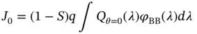
Figure 12.16 shows the DRM‐calculated EQE spectra of the CsFAPb(I,Br)3 top and Si bottom cells of the tandem structure in Figure 12.14a (solid lines), together with experimental EQE spectra reported for a 25.2% efficiency cell (open circles) [8]. The calculation results further show the variation of the EQE spectrum with the CsFAPb(I,Br)3 top‐cell thickness. To perform the EQE calculation, the perovskite α spectrum with Eg = 1.59 eV (i.e. −0.06 eV shift in Figure 12.14c) is employed. With increasing the perovskite absorber thickness, the EQE response of the top cell becomes larger, while that of the bottom cell decreases. The calculated EQE spectrum is in excellent agreement when the perovskite thickness is d = 600 nm.
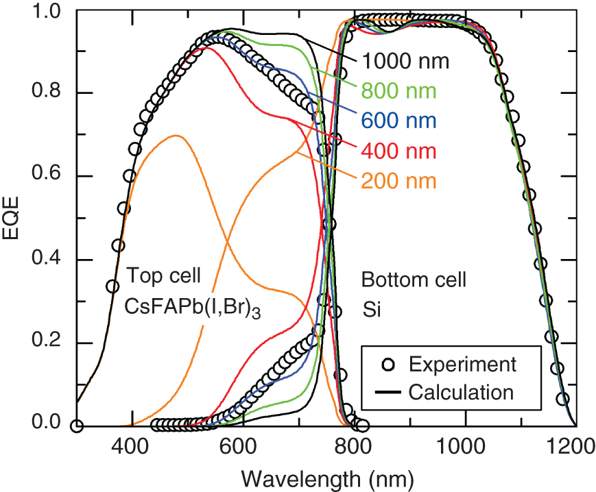
Figure 12.16 EQE spectra of the CsFAPb(I,Br)3 top cell and Si bottom cell for the tandem‐cell structure of Figure 12.14a, obtained from the DRM calculations (solid lines), together with the experimental EQE spectra (open circles) reported for a 25.2%‐efficiency cell [8]. For the calculation results, the variation of the EQE spectrum with CsFAPb(I,Br)3 thickness (200–1000 nm) is further shown. In the DRM calculation, the optical confinement factor [48] is assumed to be f = 2 and the perovskite α spectrum is adjusted to Eg = 1.59 eV (i.e. −0.06 eV shift in Figure 12.14c).
12.4.3 Maximum Efficiencies of Tandem Devices
Once the EQE spectra of the top and bottom cells are calculated, their corresponding (J0, Jsc) values can be estimated separately using Eqs. (12.16) and (12.17). By applying a simple diode equation (i.e. Eq. (12.1)), we can further calculate the J–V curve for each cell. From these J–V curves, the J–V curve of the tandem cell is determined [48]:
where Vtop(J) and Vbottom(J) are the inverse functions of Jtop(V) and Jbottom(V) calculated for the top and bottom cells, respectively. In estimating V(J) using Eq. (12.18), the current matching condition is also considered; namely, the Jsc of the tandem cell is limited by either the top cell or the bottom cell that shows lower Jsc. From the J(V) obtained from Eq. (12.18), the theoretical solar‐cell parameters and conversion efficiency of the tandem cell are obtained.
Figure 12.17 shows the mapped results of the CsFAPb(I,Br)3/Si tandem‐cell efficiency calculated by varying the top‐cell Eg and layer thickness in the cell structure of Figure 12.14a. For these calculations, the shadow loss of the front metal‐grid electrode is assumed to be zero (i.e. S = 0). In Figure 12.17a, the simulation results obtained using the true CsFAPb(I,Br)3 optical properties are shown, whereas the calculation results derived assuming the step‐function α are indicated in Figure 12.17b. The optical properties of the top cell absorber modify the maximum cell efficiency rather significantly; specifically, when an exact perovskite α is used, the optimum Eg varies with the top‐cell absorber thickness (d) due to limited light absorption. In particular, when the top cell is thin, the Jsc of the tandem cell is limited by the top cell and, with decreasing d from 1000 to 400 nm, the optimum top‐cell Eg is reduced from Eg = 1.63 to 1.53 eV in an effort to increase the top‐cell light absorption. In contrast, when a step‐function α is assumed, the light absorption in the top cell becomes unrealistically high, pushing the optimum Eg up to 1.7 eV, essentially independent of the top‐cell absorber thickness.
Figure 12.17 CsFAPb(I,Br)3/Si tandem‐cell efficiencies calculated by varying the top‐cell absorber Eg and thickness assuming (a) the experimental α and (b) the step function α for the CsFAPb(I,Br)3 absorber and (c) EQE spectra of the top and bottom cells obtained under the optimum conditions with the experimental and step‐function α spectra. The calculations are performed based on the DRM method [48] with the cell structure shown in Figure 12.14a. The open circles in (a) and (b) show the highest efficiencies obtained for each simulation at d ≤ 1000 nm. The EQE spectra obtained for these optimum conditions are shown in (c).
The open circles in Figure 12.17a,b show the highest efficiencies obtained in each simulation with d ≤ 1000 nm. Although the maximum efficiencies of these calculations are similar (η ∼ 40%), the optimum Eg differs (i.e. Eg = 1.63 eV for the true perovskite α and Eg = 1.69 eV for the step‐function α). The EQE spectra obtained for these optimum conditions are shown in Figure 12.17c, which confirms that the EQE of the top cell becomes much higher when the step‐function α is considered due to high α particularly in the band‐edge region (see Figure 12.14b).
For the experimental CsFAPb(I,Br)3/Si tandem cell, the optimum top‐cell Eg is 1.60 eV [8], with the effective thickness of 600 nm analyzed in Figure 12.16. This experimentally determined optimum Eg is indeed the best value at d = 600 nm in Figure 12.17a and thus the calculation result is consistent with the experimental result. In previous simple optical simulations [51–53], a much wider optimum Eg of ∼1.73 eV has been reported. It should be emphasized that Voc loss becomes larger in wide‐gap perovskite cells with Eg > 1.65 eV (see Figure 1.10) and a low‐Eg perovskite top cell is advantageous in realizing higher efficiencies. Accordingly, the detailed calculation is vital to accurately establish the best tandem‐cell design.
In the above analysis, the Si wafer thickness is fixed at 260 μm. When this thickness is varied, however, the optimum top‐cell Eg also varies. Figure 12.18 shows the optimum Eg of the perovskite top cell as a function of Si wafer thickness. In Figure 12.18, several results calculated for different top‐layer thicknesses in a range of 400–1000 nm are shown. If the Si wafer becomes thin, the Jsc of the bottom cell decreases and thus the Eg of the top cell widens to establish the current matching for the lower Jsc. In contrast, when the top cell is thick, there is sufficient light absorption and the Eg of the top cell increases so that the Voc gain becomes larger. In fact, for a very thick perovskite top cell (∼1 μm), a wide‐gap perovskite with Eg = 1.68 eV has been adopted [54]. As shown above, the tandem‐cell design varies with the numerous parameters and device simulation is beneficial for efficient optimization of the solar‐cell architecture.
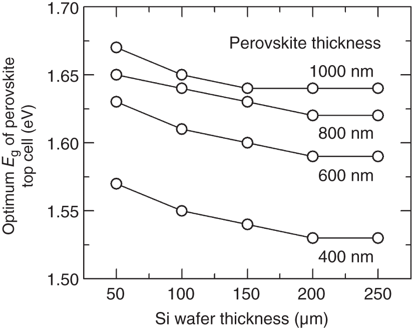
Figure 12.18 Variation of the optimum Eg for the CsFAPb(I,Br)3 perovskite top cell with Si wafer thickness in the CsFAPb(I,Br)3/Si tandem device. Several results calculated for different top‐layer thicknesses in a range of 400–1000 nm are shown.
12.4.4 Realistic Maximum Efficiency of Tandem Cell
The efficiency limit obtained for the CsFAPb(I,Br)3/Si tandem cell is ∼40% (Figure 12.17). In this calculation, however, the critical influences of cell series resistance, shadow loss of the front metal‐grid electrode, and Auger recombination in the Si absorber [33, 34] are neglected. In this section, we calculate more realistic potential efficiency by accounting for these effects.
Table 12.2 summarizes the Voc, Jsc, FF, and conversion efficiency of a CsFAPb(I,Br)3/Si tandem cell obtained under different models (assumptions). The calculation result of Model1 shows the maximum efficiency indicted by the open circle in Figure 12.17a (i.e. η = 39.55%). For this tandem cell, the Voc of the top cell is 1.38 V, while that of the bottom cell is 0.82 V. However, this bottom‐cell Voc is unrealistically high because it is calculated without considering the strong Auger recombination in the indirect Si absorber. By applying the J–V analysis method shown in Figure 11.12, the increase in J0 in the Si bottom cell due to the Auger recombination was determined based on experimental J–V characteristics reported in Ref. [41]. In particular, the J0 of the Si bottom cell can be expressed as J0 = J0,rad + J0,Aug, where J0,rad indicates the radiative recombination calculated from Eq. 12.17 and J0,Aug is the Auger recombination contribution determined experimentally. The actual values are J0,rad = 3.1 × 10⁻¹³ mA/cm2 and J0,Aug = 1.3 × 10⁻¹¹ mA/cm2, indicating that the J0 of the Si bottom cell is governed by J0,Aug. The calculation result obtained by incorporating Auger recombination in the Si cell is shown as Model2 in Table 12.2. In this case, the Voc of the bottom cell decreases to a realistic value of 0.725 V. As a result of the Si Auger recombination, the tandem efficiency is reduced by ∼2%.
In Model3, the series resistance of the Si bottom cell (Rs,bottom) is further considered by applying Eq. (11.3). For this calculation, Rs,bottom = 0.44 Ωcm2 extracted from an experimental Si heterojunction cell [41] is applied. It can be confirmed that Rs,bottom does not affect the overall result notably. In Model4, the effect of Rs in the perovskite top cell (Rs,top) has been incorporated by assuming Rs,top = 1.8 Ωcm2 obtained from the analysis of Figure 11.12. In this case, the FF decreases slightly, reducing the efficiency to 36.77%. In the final model (Model5), the shadow loss caused by the front metal‐grid electrode is considered using S = 0.023, as adopted in the experimental perovskite/Si tandem cell [8]. This model results in η = 35.93% with Jsc of 19.6 mA/cm2. In Figure 12.19, the J–V characteristics calculated from Model5 are shown. As indicated by this result, a high efficiency of ∼36% can be achieved realistically in a hybrid perovskite/Si tandem cell with the practical structure of Figure 12.14a. To realize such a high efficiency, it is necessary to suppress the Voc and FF losses in the perovskite top cell, as indicated in Figure 12.13.
Table 12.2 Maximum solar‐cell parameters obtained for a CsFAPb(I,Br)3/Si tandem cell under different assumptions.
| Model | Additional parameter | Voc (V) | Jsc (mA/cm2) | FF | η (%) |
|---|---|---|---|---|---|
| 1 | — | 2.20e) | 20.0 | 0.895 | 39.55 |
| 2a) | J0,bottom = 1.3 × 10⁻¹¹ mA/cm2 | 2.10f) | 20.0 | 0.891 | 37.63 |
| 3b) | Rs,bottom = 0.44 Ωcm2 | 2.10 | 20.0 | 0.887 | 37.46 |
| 4c) | Rs,top = 1.8 Ωcm2 | 2.10 | 20.0 | 0.871 | 36.77 |
| 5d) | S = 2.3% | 2.10 | 19.6 | 0.871 | 35.93 |
The corresponding maximum efficiency (η) is also shown. The results of Model1 correspond to those shown in Figure 12.17a.
a) J0 of the Si bottom cell is increased to simulate the strong Auger recombination observed in Si cells. The parameter value is extracted from a 24.7%‐efficient a‐Si:H heterojunction solar cell [41].
b)Series resistance of the Si bottom cell (Rs,bottom) is considered. The parameter value is extracted from a 24.7%‐efficient Si heterojunction solar cell [41].
c)Series resistance of the CsFAPb(I,Br)3 top cell (Rs,top) is considered. The parameter value is adopted from the analysis result of Table 11.1.
d)Shadow loss caused by the front metal‐grid electrode is considered. The parameter value is adopted based on an experimental CsFAPb(I,Br)3/Si tandem cell [8].
e)Voc = 1.38 V (Voc,top) + 0.82 V (Voc,bottom).
f)Voc = 1.38 V (Voc,top) + 0.72 V (Voc,bottom).

Figure 12.19 J–V characteristics of the two‐terminal CsFAPb(I,Br)3/Si tandem cell calculated from Model5 in Table 12.2. In Model5, a strong Auger recombination in the Si bottom cell, series resistances of Rs,bottom = 0.44 Ωcm2 and Rs,top = 1.8 Ωcm2, and a shadow loss of 2.3% are assumed, resulting in η = 35.93%. The corresponding J–V curves of the top and bottom cells are also shown.
12.5 Free Software for Efficiency Limit Calculation
A Windows‐based free computer software (e‐ARC software) has been developed [24] to perform maximum‐efficiency calculations of photovoltaic devices. Using this software, the efficiency limits of single and tandem devices can be calculated by applying Eq. 12.17. From this software, the EQE calculations based on the ARC method, introduced in this chapter, can also be performed. A more detailed description of the e‐ARC software package is given in Section 11.4.3. The package can be downloaded from https://unit.aist.go.jp/rpd‐envene/PV/en/service/e‐ARC_en/index_en.html, which can be found using the search term “e‐ARC AIST.”
References
- 1 Kato, Y., Fujimoto, S., Kozawa, M., and Fujiwara, H. (2019). Phys. Rev. Appl. 12: 024039.
- 2 Shockley, W. and Queisser, H.J. (1961). J. Appl. Phys. 32: 510.
- 3 Green, M.A., Dunlop, E.D., Hohl‐Ebinger, J. et al. (2020). Prog. Photovoltaics Res. Appl. 28: 629.
- 4 Shin, S.S., Yeom, E.J., Yang, W.S. et al. (2017). Science 356: 167.
- 5 Min, H., Kim, M., Lee, S.‐U. et al. (2019). Science 366: 749.
- 6 Green, M.A., Emery, K., Hishikawa, Y. et al. (2013). Prog. Photovoltaics Res. Appl. 21: 1.
- 7 Lee, Y.S., Gershon, T., Gunawan, O. et al. (2015). Adv. Energy Mater. 5: 1401372.
- 8 Sahli, F., Werner, J., Kamino, B.A. et al. (2018). Nat. Mater. 17: 820.
- 9 Bush, K.A., Palmstrom, A.F., Yu, Z.J. et al. (2017). Nat. Energy 2: 17009.
- 10 Sahli, F., Kamino, B.A., Werner, J. et al. (2018). Adv. Energy Mater. 8: 1701609.
- 11 Jošt, M., Kegelmann, L., Korte, L., and Albrecht, S. (2020). Adv. Energy Mater. 10: 1904102.
- 12 Sze, S.M. (1981). Physics of Semiconductor Devices. New York: Wiley.
- 13 Luque, A. and Hegedus, S. (2011). Handbook of Photovoltaic Science and Engineering. West Sussex: Wiley.
- 14 Correa‐Baena, J.‐P., Anaya, M., Lozano, G. et al. (2016). Adv. Mater. 28: 5031.
- 15 Fujiwara, H. and Collins, R.W. (2008). Spectroscopic Ellipsometry for Photovoltaics: Applications and Optical Data of Solar Cell Materials, vol. 2. Cham: Springer.
- 16 Nakane, A., Tampo, H., Tamakoshi, M. et al. (2016). J. Appl. Phys. 120: 064505.
- 17 Hara, T., Maekawa, T., Minoura, S. et al. (2014). Phys. Rev. Appl. 2: 034012.
- 18 Shirayama, M., Kadowaki, H., Miyadera, T. et al. (2016). Phys. Rev. Appl. 5: 014012.
- 19 Fujiwara, H., Kato, M., Tamakoshi, M. et al. (2018). Phys. Status Solidi A 215: 1700730.
- 20 Fujiwara, H. and Collins, R.W. (2018). Spectroscopic Ellipsometry for Photovoltaics: Fundamental Principles and Solar Cell Characterization, vol. 1. Cham: Springer.
- 21 Koida, T., Kondo, M., Tsutsumi, K. et al. (2010). J. Appl. Phys. 107: 033514.
- 22 Bhachu, D., Waugh, M.R., Zeissler, K. et al. (2011). Chem. Eur. J. 17: 11613.
- 23 Macleod, H.A. (2010). Thin‐Film Optical Filters. New York: CRC Press.
- 24 The e‐ARC software has been developed by the research collaboration of Gifu University and AIST. This software can be downloaded at the web site of https://unit.aist.go.jp/rpd‐envene/PV/en/service/e‐ARC_en/index_en.html. This web site can be found using “e‐ARC AIST” as key words (accessed 01 April 2021).
- 25 Yao, J., Kirchartz, T., Vezie, M.S. et al. (2015). Phys. Rev. Appl. 4: 014020.
- 26 Tress, W., Marinova, N., Inganäs, O. et al. (2014). Adv. Energy Mater. 5: 1400812.
- 27 Tvingstedt, K., Malinkiewicz, O., Baumann, A. et al. (2014). Sci. Rep. 4: 6071.
- 28 Nishiwaki, M., Nagaya, K., Kato, M. et al. (2018). Phys. Rev. Mater. 2: 085404.
- 29 Nagaya, K., Fujimoto, S., Tampo, H. et al. (2018). Appl. Phys. Lett. 113: 093901.
- 30 Green, M.A., Hishikawa, Y., Dunlop, E.D. et al. (2019). Prog. Photovoltaics Res. Appl. 27: 3.
- 31 Jiang, Q., Chu, Z., Wang, P. et al. (2017). Adv. Mater. 29: 1703852.
- 32 Liu, Z., Krückemeier, L., Krogmeier, B. et al. (2019). ACS Energy Lett. 4: 110.
- 33 Tiedje, T., Yablonovitch, E., Cody, G.D., and Brooks, B.G. (1984). IEEE Trans. Electron Devices 31: 711.
- 34 Green, M.A. (1984). IEEE Trans. Electron Devices 31: 671.
- 35 Green, M.A. (1998). Solar Cells: Operating Principles, Technology and System Applications. Kensington: University of New South Wales.
- 36 Gabor, A.M., Tuttle, J.R., Bode, M.H. et al. (1996). Sol. Energy Mater. Sol. Cells 41–42: 247.
- 37 Ringel, S.A., Smith, A.W., MacDougal, M.H., and Rohatgi, A. (1991). J. Appl. Phys. 70: 881.
- 38 Wang, W., Winkler, M.T., Gunawan, O. et al. (2014). Adv. Energy Mater. 4: 1301465.
- 39 Werner, J., Nogay, G., Sahli, F. et al. (2018). ACS Energy Lett. 3: 742.
- 40 Stolterfoht, M., Wolff, C.M., Márquez, J.A. et al. (2018). Nat. Energy 3: 847.
- 41 Taguchi, M., Yano, A., Tohoda, S. et al. (2014). IEEE J. Photovoltaics 4: 96.
- 42 Taguchi, M., Terakawa, A., Maruyama, E., and Tanaka, M. (2005). Prog. Photovoltaics Res. Appl. 13: 481.
- 43 Fujiwara, H. and Kondo, M. (2007). J. Appl. Phys. 101: 054516.
- 44 Wynands, D., Erber, M., Rentenberger, R. et al. (2012). Org. Electron. 13: 885.
- 45 Holman, Z.C., Filipič, M., Descoeudres, A. et al. (2013). J. Appl. Phys. 113: 013107.
- 46 Baker‐Finch, S.C. and McIntosh, K.R. (2011). Prog. Photovoltaics Res. Appl. 19: 406.
- 47 Altazin, S., Stepanova, L., Werner, J. et al. (2018). Opt. Express 26: A579.
- 48 Nishigaki, Y., Nagai, T., Nishiwaki, M. et al. (2020). Sol. RRL 4: 1900555.
- 49 Watanabe, K., Matsuki, N., and Fujiwara, H. (2010). Appl. Phys. Express 3: 116604.
- 50 Matsuki, N. and Fujiwara, H. (2013). J. Appl. Phys. 114: 043101.
- 51 Yu, Z.J., Leilaeioun, M., and Holman, Z. (2016). Nat. Energy 1: 16137.
- 52 Lal, N.N., Dkhissi, Y., Li, W. et al. (2017). Adv. Energy Mater. 7: 1602761.
- 53 Hossain, M.I., Qarony, W., Ma, S. et al. (2019). Nanomicro Lett. 11: 58.
- 54 Hou, Y., Aydin, E., De Bastiani, M. et al. (2020). Science 367: 1135.