17
Perovskite‐Based Tandem Solar Cells
Klaus Jäger1 and Steve Albrecht2
1Helmholtz‐Zentrum Berlin für Materialien und Energie, Department of Optics for Solar Energy, Albert‐Einstein‐Straße 16, 12489 Berlin, Germany
2Helmholtz‐Zentrum Berlin für Materialien und Energie, Young Investigator Group Perovskite Tandem Solar Cells, Kekuléstraße 5, 12489 Berlin, Germany
17.1 Introduction
As thoroughly discussed in the previous chapters, perovskite solar cells made tremendous progress in recent years. However, as for all single‐junction solar cells, their power conversion efficiency () is limited by the detailed balance limit [1], as discussed in Chapter 12. Figure 17.1a shows the two major loss mechanisms of single‐junction solar cells. The solar cell is based on a semiconductor, which is transparent for photons with energies below the semiconductor bandgap. This loss is called below‐bandgap loss. For silicon (Si), with a bandgap of 1.1 eV, corresponding to a wavelength of 1127 nm, this loss accounts for around 19% of the total solar irradiance. On the other hand, the maximum energy that the solar cell can utilize per absorbed photon is slightly lower than the bandgap. Therefore, the usable energy is considerably below the available energy from the photons, as illustrated in Figure 17.1a, which is called thermalization loss and accounts for at least 33% of the available energy for 1.1 eV semiconductor bandgap.
The thermalization loss can be reduced considerably when combining more or two solar cells in multi‐junction solar cells. Tandem solar cells, where two solar cells are combined, are constructed such that incident sunlight first hits the top cell with the higher bandgap. The fraction of the solar spectrum with energies below the top cell bandgap can pass the top cell and can be absorbed by the bottom cell. Because the high energy photons are utilized by the top cell, the overall thermalization losses can be reduced considerably, as illustrated in Figure 17.1b.
Figure 17.2 shows absorption spectra of the absorbers in (a) a state‐of‐the‐art silicon solar cell with pyramidal textures on both sides and (b) a state‐of‐the art monolithic1 perovskite‐silicon tandem solar cell with a flat perovskite top cell and a pyramidally back‐textured silicon cell. We see that in (b) the absorption is split between the two sub cells. Short‐wavelength light is absorbed in the top cell, while long‐wavelength light traverses the top cell and is absorbed in the bottom cell. The pyramidal texture at the back increases the average light path and therefore increases the absorption in the silicon wafer for wavelength longer than ∼900 nm. Because of manufacturing issues, most perovskite top cells still are flat. This leads to interferences, which are visible in Figure 17.2b. Using textures is one way of light management, which will be discussed in Section 17.5.
![Schematic illustration of the AM1.5g solar spectrum [2] and the two most important losses for (a) protect single-junction and (b) tandem solar cells. As bandgap for the single-junction cell and the bottom cell of the tandem cell, 1.1 eV (1127 nm) is chosen, which corresponds to the bandgap of silicon. As top-cell bandgap, 1.71 eV are chosen, which is the optimal bandgap for series-connected two-terminal devices.](https://imgdetail.ebookreading.net/2023/10/9783527347292/9783527347292__9783527347292__files__images__c17f001.png)
Figure 17.1 The AM1.5g solar spectrum [2] and the two most important losses for (a) single‐junction and (b) tandem solar cells. As bandgap for the single‐junction cell and the bottom cell of the tandem cell, 1.1 eV (1127 nm) is chosen, which corresponds to the bandgap of silicon. As top‐cell bandgap, 1.71 eV are chosen, which is the optimal bandgap for series‐connected two‐terminal devices.
Source: A.S.T.M.S. G173‐03 [2].
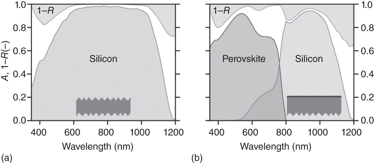
Figure 17.2 Example of (a) a simulated absorption spectrum of the silicon absorber in a state‐of‐the‐art silicon heterojunction (SHJ) solar cell and 1 − R spectrum of this cell with pyramidal textures on both sides. Example of (b) simulated absorption spectra of the perovskite and silicon absorbers in a state‐of‐the‐art silicon monolithic perovskite‐silicon tandem solar cell based on a back‐textured SHJ cell and 1 − R spectrum of this tandem cell. The detailed layer stack of the tandem cell is given in Ref. [3]. The SHJ cell in (a) is based on the same design but with an additional pyramidal texture on front and a 100 nm thick indium tin oxide (ITO) layer as front electrode. All simulations were performed with the package GENPRO4 [4], which is based on the net‐radiation method and ray tracing.
Source: Jäger et al. [3].
In this chapter we will discuss tandem solar cells with a perovskite‐based top cell. In Section 17.2 we discuss different types (or architectures) of tandem solar cells and review the general efficiency limits for tandem solar cells in Section 17.3. In Section 17.4 we discuss, why perovskites are well‐suited for tandem solar cells. Section 17.5 is devoted to two‐experimental results of perovskite‐based tandem solar cells. In Section 17.6 we briefly discuss energy yield calculations before we conclude the chapter with the outlook and guidelines in Section 17.7. Perovskite–perovskite tandem solar cells are discussed in Chapter 18.
17.2 Architectures of Tandem Solar Cells
Tandem solar cells can be manufactured in various different architectures, as illustrated in Figure 17.3. For all these concepts light is considered to arrive at the solar cell from top, hence, it reaches first the solar cell with the higher bandgap. The most common concepts are monolithic two‐terminal (2T) tandem solar cells, shown in Figure 17.3a, and four‐terminal (4T) tandems solar cells Figure 17.3b,c.
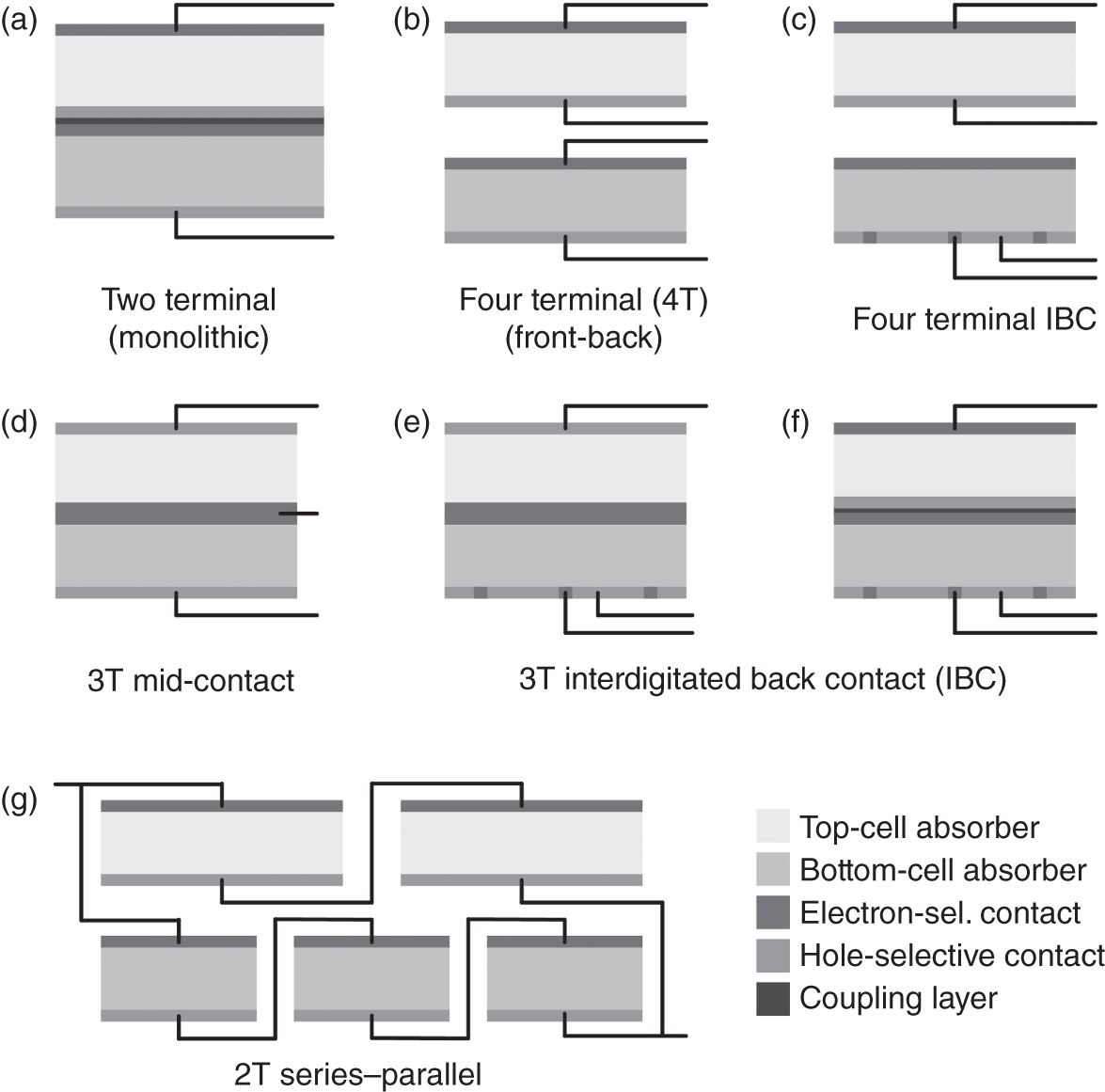
Figure 17.3 Illustrating different architectures for tandem solar cells. For all, light is illuminating the cell from top. The most common concepts are (a) monolithic two‐terminal (2T) and (b)–(c) four‐terminal (4T) cells. (d)–(f) Also three‐terminal (3T) concepts are investigated, where we distinguish between (d) mid‐contacted cells and (e)–(f) cells with interdigitated back contacts (IBC). (g) Also, series‐parallel connected tandem cells a considered. For all concepts light arrives on the cells from top.
Source: Based on Rienäcker et al. [5].

Figure 17.4 (a) Current density (J) – voltage (V) characteristics for single‐junction solar cells under AM1.5 illumination for cells with a large bandgap “t” and a small bandgap “b” as well as the J–V characteristics of a monolithic series‐connected tandem solar cell consisting of these two subcells “t+b.” (b) The equivalent circuit of a monolithic series‐connected tandem solar cell, where each subcell consists of a photocurrent source Iph, a diode with diode/dark current ID, series resistance Rs and parallel resistance Rp. Further, the resistance Rj at the junction between the two subcells is considered.
Source: Modified from Smets et al. [6].
17.2.1 Monolithic Two‐Terminal Solar Cells
In monolithic two‐terminal cells the two subcells are electronically connected in series. To understand, how such a solar cell works, we look at Figures 17.4 and 17.5, where we follow Ref. [6]. Figure 17.4a shows current density (J) – voltage (V) characteristics for single‐junction solar cells under AM1.5 illumination for cells with a large bandgap “t” and a small bandgap “b” as well as the J–V characteristics of a monolithic series‐connected tandem solar cell consisting of these two subcells “b+t.”
To understand why the combined J–V curve looks as plotted in the graph, we take a look at Figure 17.4b, which shows an equivalent circuit of the tandem cell: in series connection, the voltages add up and the same current flows through both cells – it is determined by the subcell generating the lower current. This important property of monolithic tandem cells is called current matching and negatively affects the overall performance if the currents generated in the two subcells differ significantly. We will discuss this topic in more detail in Section 17.5.
Figure 17.5 sketches a band diagram of a tandem solar cell (a) in the dark and (b) under illumination. In (a) the situation is drawn under thermal equilibrium, meaning that the Fermi energy EF is constant across the whole device. Here we assume that the two solar cells are homojunctions, hence their respective bandgaps are constant across the whole junction. In real devices, often different materials with different bandgaps will be used, hence the band diagram looks more complicated.

Figure 17.5 Schematic band diagram of tandem solar cells (a) in the dark at thermal equilibrium and (b) under illumination at the maximum power point (MPP). In (a) the energy levels of the valence band EV and conduction band EC are depicted for both top and bottom cells. Further, the Fermi energy EF and the bandgaps Eg are depicted. In (b), quasi‐Fermi level splitting is observed in both subcells, with the quasi Fermi levels EFn and EFp for electrons and holes, respectively. In the ideal case the voltages add up without voltage loss across the interface, where q denotes the elementary charge. Therefore, efficient recombination of electrons and holes at the interface between the two subcells is required.
Source: Modified from Smets et al. [6].
Under illumination, high‐energy (short‐wavelength) photons are absorbed by the top cell while low‐energy (long wavelength) photons can pass through the top cell and are absorbed in the bottom cell, as illustrated in Figure 17.5b. In both subcells the Fermi level separates into quasi‐Fermi levels for electrons and holes, respectively, as shown in Figure 17.5b. In the ideal case the two voltages add up, which is also depicted. Therefore, it is necessary, that electrons and holes can combine efficiently at the interface between the top and bottom cells. This can be either done with tunnel junctions or with a (metallic) recombination layer. Both concepts are discussed in Section 17.5.
17.2.2 Four‐Terminal Tandem Solar Cells
Figures 17.3b,c sketch four‐terminal (4T) tandem solar cells – the other common tandem‐cell concept. As in monolithic 2T solar cells, light passes first through the high‐bandgap top cell and then through the low‐bandgap bottom cell. In contrast to 2T cells, here each subcell has its own electric connections and can be operated independently from the other subcell. Therefore, both subcells can be operated at their respective maximum power points (MPPs) – no matter how the light is distributed between the two subcells.
This makes 4T cells much less sensitive to changes in the spectrum of the light, which illuminates the cell. Hence, the overall energy yield in principle can be higher than with 2T solar cells. However, for the bottom contact of the top cell and for the top contact of the bottom cell two additional contacting layers need to be established for an efficient lateral transport of the charge carriers. Such contacts can be transparent conducting oxide (TCO) layers such as indium tin oxide, zinc oxide or tin oxide. For wafer‐based silicon solar cells, also a metal grating system can be used. In any case, optical losses because of parasitic absorption and/or shading by metal fingers will be larger than for 2T devices, where only vertical transport of charge carriers is required between the two subcells. If the bottom cell is an interdigitated back‐contact cell, as sketched in Figure 17.3c, these losses can be slightly reduced.
Further, every module has four connections, therefore the number of cables in a photovoltaic (PV) system consisting of 4T modules roughly doubles, which increases the balance of system (BOS) costs of the PV system.
Several numerical studies compared the energy yield of photovoltaic systems based on two‐terminal and four‐terminal tandem solar cells with a perovskite top cell – we will review a few of them in Section 17.6.
17.2.3 Other Concepts
As discussed above, the major drawback of two‐terminal tandem solar cells is current mismatch, which means that the overall performance goes down when the current densities generated in the top and bottom cells differ. On the other hand, four‐terminal cells suffer from higher optical losses because of the contacting layers on bottom of the top cell and on top of the bottom cell.
Figure 17.3d–f shows sketches of three‐terminal (3T) tandem solar cells, which aim to combine the advantages of the two concepts by adding a third terminal to a 2T cell [5]. The third terminal matches the currents of the two subcells and therefore overcomes the performance losses due to current mismatch. The two subcells are monolithically connected. Therefore, optical losses are less a problem than in 4T cells.
Figure 17.3d illustrates a mid‐contacted three‐terminal solar cell, where the third terminal connects to the back of the top cell and the front of the bottom cell. However, also this concept needs a contacting layer which ensures sufficient lateral transport. If a TCO is used, lateral transport can be controlled by the layer thickness as well as by the conductivity – both measures increase parasitic absorption.
If the bottom cell is designed as interdigitated‐back‐contacted cell with both the electron‐ and hole‐selective contacts at the back, the optical losses are not larger than in 2T cells. Such 3T cells can be designed as two anti‐series connected diodes with a common ground (Figure 17.3e) or as series‐connected diodes with a coupling layer (Figure 17.3f). The power output of such 3T solar cells can be almost as high as for 4T solar cells [5].
Another concept is the series–parallel connected tandem solar cell, which is sketched in Figure 17.3g [7]. When two cells are connected in parallel, their voltages have to be matched for proper operation. To achieve this in a tandem configuration, where two types of cells with different bandgaps are used, n1 top cells and n2 bottom cells are connected in series, respectively, such that their string voltages roughly match, n1 × V1 ≈ n2 × V2. These two strings are then connected in parallel. The cell voltage only depends weakly (logarithmically) on the illumination, hence the voltages of the two strings are roughly independent from the illumination. Therefore, series–parallel connected tandem solar cells are much less susceptible to the illumination conditions than monolithic two‐terminal cells. As a consequence, the bandgaps of the top and bottom cell materials are much less constraint than for monolithic 2T cells. Further, PV modules based on this concept would only have two connections which is an advantage with respect to 3T and 4T concepts. However, they would still be sensitive toward spectral changes, which naturally occur for outdoor illumination as discussed in Section 17.6.
17.2.4 Bifacial Solar Cells
At the end of this section we briefly discuss the concept of bifacial solar cells and solar modules, which not only can utilize light that is impinging on the front side of the solar module, but also light impinging at the solar module back. Depending on the reflectivity of the ground, this can significantly increase the energy yield over the year. For example, a study by Tillmann et al. showed that more than 10% of all the photon power incident on the solar module arrives at the back side for standard PV‐field configurations, when the reflectivity of the ground is assumed to be 30% [8]. Because of the rise of new technologies for silicon solar cells, such as the passivated emitter rear contact concept discussed in Section 17.5.1, bifacial solar cells are expected to have a market share of around 50% by 2029 [9].
Bifacial tandem solar cells in a four‐terminal configuration can be used just as standard monofacial cells, because the two subcells operate separately from each other. Hence, the additional light on the back side will only increase the current density of the bottom cell, shifting the MPP of the bottom cell with respect to a monofacial cell. In contrast, for monolithic tandem solar cells the additional current density at the bottom requires a change of design to achieve current matching, such that the current density in the top cell increases. We can achieve this by increasing the thickness of the absorber layer in the top cell, by using top cell materials with lower bandgaps or by using more advanced light management techniques, as discussed in Section 17.5. Finally, because of changing illumination conditions (position of the sun, clouds, etc.) the ratio between front and back‐side illumination can vary throughout the day and the year.
Energy yield analyses, explained in Section 17.6, can help to find the best band gap/thickness combination for the top cell (under the assumption that the bottom cell parameters are fixed, as e.g. for silicon solar cells). Further, these analyses can be used to assess estimate the differences in energy yield for 4T and 2T tandem cells both in monolithic and bifacial configurations.
17.3 Efficiency Limits of Multi‐Junction Solar Cells
In this section we review the theoretical efficiency limits for four‐ and two‐terminal tandem solar cells and briefly look at cells with more than two junctions. The theoretical efficiency limit for single‐junction solar cells was established by the seminal work of Shockley and Queisser in 1961 using the detailed balance approach [1, 10]. For four‐terminal cells the efficiencies of the two subcells can be maximized independently; only the bandgap of the top cell affects the short‐circuit current density of the bottom cell. For two‐terminal cells, the derivation is more complex because the two subcells are electrically connected.
17.3.1 Efficiency Limit for Four‐Terminal Tandem Solar Cells
For four‐terminal cells we can follow the derivation by De Vos from 1980 Ref. [11]. The overall efficiency η4T is given by

where Et and Eb denote the bandgap energies of the top and bottom cells, respectively, and pt and pb denote the power densities at the respective MPPs. Finally, pin denotes the incident power density, which is 1000 W/m2 for the standardized AM1.5g solar spectrum, which we use for this derivation [2]. For the whole section we assume Et > Eb.
The maximum power density for the top cell is given by
where the maximum can be found numerically. The current density – voltage characteristic is based on the Shockley equation, which describes an ideal diode,
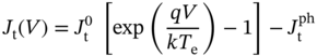
with the dark current density ![]() , the photocurrent density
, the photocurrent density ![]() the elementary charge q, the Boltzmann constant k and the temperature of the environment of the solar cell Te, which is set to 25 °C for solar cell standard testing conditions (STCs) [12]. To calculate the dark current density, we use the detailed balance assumption, which assumes that the solar cell behaves as a black body for wavelengths up to the bandgap and is fully transparent for longer wavelengths and that the black body radiation is driven by radiative recombination in the solar cell,
the elementary charge q, the Boltzmann constant k and the temperature of the environment of the solar cell Te, which is set to 25 °C for solar cell standard testing conditions (STCs) [12]. To calculate the dark current density, we use the detailed balance assumption, which assumes that the solar cell behaves as a black body for wavelengths up to the bandgap and is fully transparent for longer wavelengths and that the black body radiation is driven by radiative recombination in the solar cell,
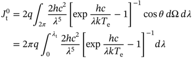
with the Planck constant h, the speed of light c and the solid angle element dΩ = sin θdθ dφ. The factor 2 arises from the fact that the solar cell is assumed to emit from both front and back sides. The factor cosθ arises from Lambert's cosine law of emission. The wavelength λt is given by λt = hc/Et. More details can be found in Ref. [6], chapter 10.
For the bottom cell Eqs. (17.2)–(17.4) hold as well, the subscript t needs just to be only replaced by b.
The photocurrent density for the top cell is given by
where the first term is the photocurrent density due to solar illumination with the spectral photon flux Φph, λ and the second term arises from the blackbody emission from the bottom cell, cut off at the bandgap of the top cell (the bottom cell also emits blackbody radiation between λt and λb, but this cannot be utilized by the top cell).
For the bottom cell, we find
where the first term is the photocurrent density due to solar illumination, which passes through the top cell with the spectral photon flux Φph, λ and the last term arises from the blackbody emission from the top cell.
The second term JLC in Eq. 17.6 accounts for luminescence coupling (LC, also called luminecent coupling): in a high‐quality top cell the part of the generated current ![]() , which is not utilized electrically, can lead to radiative recombination and hence to emission of light by the top cell. A fraction of this light reaches the bottom cell, where it can be absorbed. A simple expression for the additional current density generated in the bottom cell is given by [13, 14]
, which is not utilized electrically, can lead to radiative recombination and hence to emission of light by the top cell. A fraction of this light reaches the bottom cell, where it can be absorbed. A simple expression for the additional current density generated in the bottom cell is given by [13, 14]
with the luminescent‐coupling efficiency ηLC. No further conversion factors are needed, because one electron–hole pair in the top cell, which recombines radiatively, leads to the emission of one photon, which may generate one electron–hole pair in the bottom cell. ηLC might also depend on the bias voltage Vt of the top cell, which, however, is out of the scope of this book [13]. In principle also LC from the bottom cell into the top cell should be considered. However, as we may safely assume that the light is emitted with energies close to the bandgap, light emitted by the bottom cell has energies below the top‐cell bandgap and cannot be utilized.
Figures 17.6a,b shows the theoretical efficiency limit for four‐terminal cells as a function of the top‐ and bottom‐cell bandgaps. For 4T cells the efficiencies of the top and bottom subcells can be maximized independently of each other for each combination of bandgaps. Without luminescence coupling, shown in Figure 17.6a, the maximum PCE is 45.2% with top and bottom bandgap energies of 1.73 and 0.94 eV, respectively. This value is significantly higher than the detailed balance limit for single junction solar cells, which is slightly above 30%. For 4T cells, maximal luminescence coupling (ηLC = 100%) only would change the picture slightly, as shown in Figure 17.6b, where the maximum efficiency is 45.4% at 1.73 eV top‐ and 0.95 eV bottom‐cell bandgaps. The little effect of LC can be understood as follows: in a 4T cell, the top cell operates at its MPP with a current density Jt close to ![]() . Hence,
. Hence, ![]() and subsequently JLC are very small.
and subsequently JLC are very small.

Figure 17.6 The theoretical efficiency limits for tandem solar cells as functions of the top and bottom cell bandgap energies. Results are shown for four‐terminal cells (a) without and (b) with ideal luminescence coupling (LC efficiency ηLC = 100%): and for two‐terminal cells (c) without and (d) with 100% LC. In all plots the maximum is marked by a star; the purple line denotes a bottom‐cell bandgap of Eb = 1.1 eV, for which section plots are shown in Figure 17.7.
17.3.2 Efficiency Limit for Two‐Terminal Tandem Solar Cells
For two‐terminal cells, the two subcells cannot be treated independently because of their electrical series connection. As a consequence, the same current density flows through both subcells. Hence, we write
where the maximum power density is given by
In contrast to Eq. 17.2, here the voltages V have to be treated as dependent variables – hence the Shockley equation 17.3 must be inverted. Therefore, identifying the maximum power is numerically more involved than for 4T solar cells. The dark current density and the photocurrent densities can be calculated as in the 4T case using Eqs. (17.4)–(17.6).
Figure 17.6c shows the theoretical efficiency limit for two‐terminal tandem solar cells with no and 100% luminescence coupling. Without LC, the maximum PCE is 44.8% with top and bottom bandgap energies of 1.63 and 0.96 eV, respectively. While this limit is only slightly below that of 4T cells, the sweet spot is much smaller for this architecture. Especially, the top‐cell bandgap strongly affects the overall efficiency: at higher top‐cell bandgaps, the top photocurrent density decreases, increasing the potential photocurrent density of the bottom cell. However, this increase cannot be utilized because of current matching. On the other hand, 1.63 eV is closer to the bandgap of high‐performance perovskites than 1.73 eV, which is the optimum for 4T cells. If 100% LC was occurring, as shown in Figure 17.6d, the maximum would be 45.2% at 1.58 eV top‐ and 0.94 eV bottom‐cell bandgaps. For top‐cell bandgaps below the maximum, Figure 17.6d looks almost like for 4T cells, meaning that luminescence coupling can (partially) compensate for the disadvantages of 2T cells.
Figure 17.7 shows the efficiency limit for 2T and 4T tandem solar cells as functions of the top‐cell bandgap for a bottom‐cell bandgap of 1.1 eV, which corresponds to the bandgap of silicon – the semiconductor on which most solar cells are based on. While the top‐cell bandgap hardly affects the overall efficiency for 4T cells, 2T cells without luminescence coupling are very susceptible to changes of the top‐cell bandgap with a very narrow maximum. This also makes them more sensitive to spectral changes in the illumination, which naturally occur throughout the course of time. We will discuss this topic in Section 17.6. For ideal luminescence coupling (ηLC = 100%), the maximum efficiency is almost as high as for 4T cells, when the top‐cell bandgap is below the maximum: in this regime the 2T‐cells are bottom‐cell limited, which can be partially compensated by the additional current from luminescence coupling. However, for larger wavelength, the 2T cells are top‐cell limited and luminescence coupling has no added value. As discussed above, luminescence coupling can only improve 4T cells slightly.
Experimentally, luminescence coupling is not a relevant effect in perovskite‐based tandem solar cells yet. For perovskite solar cells, external luminescence quantum efficiencies of up to 15% were reported as of summer 2020 [15–20]. For III–V multi‐junction solar cells, where the strongest LC is observed, efficiencies of 33% were reported [21].
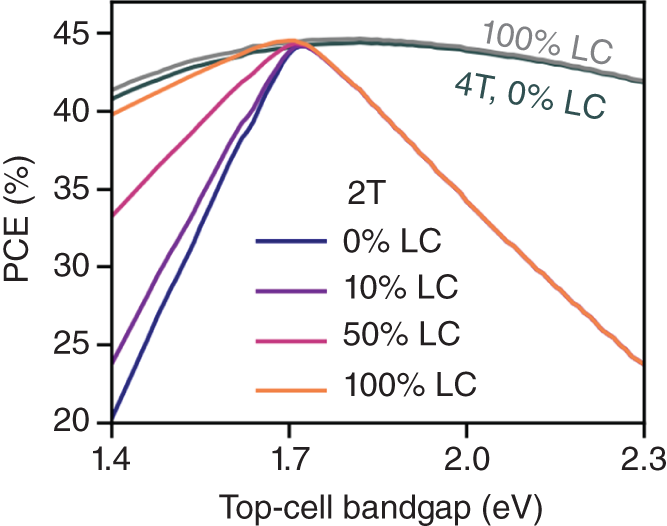
Figure 17.7 Efficiency limits for 2T and 4T tandem solar cells as a function of the top‐cell bandgap for different luminescence coupling efficiencies, when the bottom‐cell bandgap is 1.1 eV, which corresponds to the bandgap of silicon.
Note that the theoretical limit for silicon solar cells (29.4%) is a few per cent below the detailed balance limit for 1.1 eV [22]. Silicon is an indirect semiconductor, therefore recombination happens mainly via Auger processes, while radiative recombination, which is assumed in the Shockley–Queisser limit, hardly occurs.
17.3.3 Efficiency Limit for Cells with More Junctions
As we have seen, tandem solar cells can yield higher PCEs than single‐junction solar cells, because the top cell with the higher bandgap can utilize the energy of high‐energy photons more effectively. The efficiency can be increased even more by building solar cells with more than two junctions.
Figure 17.8 shows the bandgap utilization and the efficiency limits for cells with one, two, three, four, and infinitely many junctions according to data from Martí and Araújo [23]. If the sunlight is not concentrated, a cell consisting of one, two, three, or four junctions would yield a PCE of 32.5%, 44.3%, 50.1%, and 54.0%, respectively. In the limit of infinitely many junctions 65.4% of the incident sunlight would be converted into electricity. The additional gain decreases with every additional junction the optimal number of junctions therefore finally depends on the economics: is the cost of additional junctions outweighed by the gain in performance. Note that the efficiency limit for tandem cells (44.3%) slightly differs from the limits presented in Figure 17.7. The reason for this is probably different spectral data for the AM1.5 spectrum as well as other numerical effects.
17.4 Perovskites as Tandem Solar Cell Materials
The development of tandem solar cells based on mature commercial solar cell technologies such as silicon (Si) or copper indium gallium selenide (CIGS) poses several requirements on the properties of the partnering subcell. The most obvious one is a suitable complementary bandgap (see Figure 17.6) with high absorption for photons with energies exceeding the bandgap and very low absorption for photons with energies below the band gap. The material should with a very sharp absorption onset, which reflects low energetic disorder, i.e. a low Urbach energy. In addition, to achieve high power conversion efficiencies (PCEs), two‐terminal cells require a suitable electrical connection of the subcells and compatible processing of the layer stack. Moreover, general and economical aspects must be considered, for example material abundance, ease of processing, compatibility with existing fabrication lines, market readiness and cost effectiveness.
Because of their easily tunable bandgap through compositional engineering, metal‐halide perovskites are prominent candidates for perfectly adjustable top cells, with bottom cells made from Si, CIGS, or low band‐gap perovskites with Sn–Pb compositions. Besides the tunable bandgap, metal‐halide perovskites also absorb strongly at energies above the bandgap and weakly below the bandgap energy [24]. Therefore, already a perovskite layer of around 500 nm thickness absorbs a large fraction of the incident light during a single pass and enables high transmission of near‐infrared light to the bottom cell. In addition, a variety of deposition techniques can be applied to yield perovskite films with high optoelectronic quality: the different deposition techniques include solution processes like spin coating, inkjet printing and blade or slot‐die coating as well as vacuum processes like thermal co‐evaporation or a hybrid process combining different steps and processes [25]. The variety of different deposition techniques allows to cover the underlying subcell conformally, independent of the nano roughness of e.g. CIGS or the pyramidal microtexture of typical silicon solar cells. The defect tolerance of metal‐halide perovskites enables high‐efficiency solar cells at manageable requirements on material purity and process as well as equipment costs, especially with the low processing temperatures needed. Because of this combination, highly efficient tandem modules at reasonable costs will be available in the near future [26, 27].
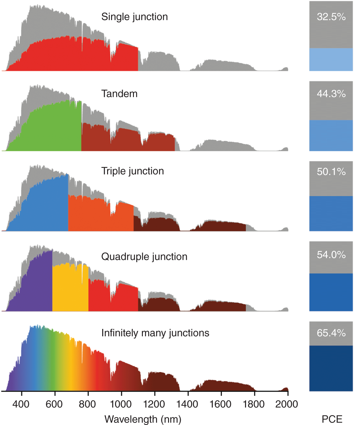
Figure 17.8 Spectral utilization for solar cells with different numbers of junctions and corresponding power‐conversion efficiencies (PCE) according to the detailed balance limit. The data are taken from Ref. [23] for non‐concentrated sunlight. Optimal bandgaps for single junction: 1.13 eV; tandem: 0.94 and 1.64 eV; triple junction: 0.71, 1.16, and 1.83 eV; quadruple junction: 0.71, 1.13, 1.55, and 2.13 eV. For maximum concentration, the efficiency limits would be higher, approaching the thermodynamic limit of 86% for infinitely many junctions.
Source: Data from Martí and Araújo [23].
The bandgap of perovskites can be tuned ranging from 1.2 to 2.3 eV by appropriately choosing the monovalent cations (methyl ammonium [MA], Cs, formamidinium [FA]), anions (I, Br, Cl), metals (Pb, Sn), and mixtures thereof [28]. On the one hand, increasing the bandgap leads to a blue‐shifted absorption edge and hence a lower photogenerated current, but on the other hand it leads to an increased open circuit voltage in solar cells. The optimal trade‐off between current and voltage depends on the architecture (i.e. two‐terminal or four‐terminal, as discussed in Section 17.3). However, a substantial scientific challenge is to enable good electrical quality and photostability over a wide range of perovskite compositions and subsequently the bandgap. In this context, the Voc‐to‐bandgap loss is an important metric to quantify the electrical quality of the perovskite absorber.
One part of the Voc‐to‐bandgap loss consists of unavoidable radiative recombination of free charges in the absorber layer, when it is in equilibrium with its surrounding. In this detailed balance limit, the solar cell emits black body radiation according to its temperature and band gap, as discussed in Section 17.3. Additionally, non‐radiative losses caused by trap‐assisted recombination in the perovskite bulk and primarily at interfaces significantly reduce the Vocs reported in experiment as compared to the detailed balance limit (see e.g. [6], section 7.3). A specific property of metal‐halide perovskites, which can be related to the Voc‐to‐bandgap loss is the crystalline‐phase instability observed for certain compositions.
Figure 17.9 shows experimentally measured open circuit voltages as a function of the material bandgap and reveals two main features: In general, the Voc follows the bandgap between 1.45 and 1.65 eV with high Voc values well above 90% of the respective detailed balance limit. However, for bandgaps above 1.65 eV, the reported Voc values are not increasing linearly with bandgap. In this bandgap range, which is of particular interest for tandem applications, the anion site of the perovskites is typically occupied by a mixture of iodine (I) and bromium (Br). In particular high Br contents were earlier reported to lead to phase instability [34], which induces additional traps and therefore nonradiative recombination centers. A reduction of these trap‐induced recombination requires additional efforts in compositional engineering [35, 36] and recently some publications have reported high Voc values for that bandgap region [29, 30]. In addition to adjusting the bulk properties of the perovskite, the charge‐selective contacts, which are well suited for the range between 1.45 and 1.65 eV may induce losses at higher bandgaps, which for example are caused by energetic misalignment. Thus, one of the main challenges for approaching the theoretical tandem efficiency limits with perovskite top cells is a reduction of non‐radiative losses and the improvement of phase stability at higher bandgaps, to reach open circuit voltages above 90% of the value from the respective detailed balance limit.
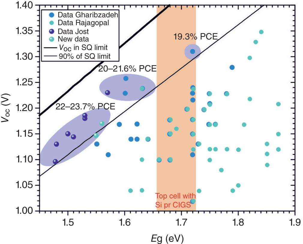
Figure 17.9 Experimentally reported open‐circuit voltages plotted as function of perovskite band‐gap. Data are collected from Gharibzadeh et al Ref. [29], Rajagopal et al. [30], and Jošt et al. [31]. In addition, new data for high efficiency results are included [32, 33]. As comparison, the detailed balance (SQ) limit and 90% of it are shown as well. The round colored areas denote efficiencies reached with the corresponding compositions (band gaps) and the band gap regime for optimized top cells with silicon and CIGS (assuming a band gap of 1.1 eV for both) bottom‐cells is also indicated.
Sources: Data from Gharibzadeh et al. [29]; Rajagopal et al. [30]; Jošt et al. [31]; Zheng et al. [32]; Zhu et al. [33].
17.5 Experimental Results on Perovskite‐Based Tandem Solar Cells
The first reports on four‐terminal perovskite/silicon [37] and perovskite/CIGS [38] tandem solar cells were published by the end of 2014. In 2015, first reports on two‐terminal tandem cells followed for both technologies [39, 40]. Since then, the two tandem technologies underwent a fascinating improvement within a short timescale. With PCEs below 14% for perovskite/silicon (both 2T and 4T) and 18% or 11% for perovskite/CIGS for 4T or 2T tandems, respectively, all reported first tandem PCEs were well below those of best single‐junctions, which is the benchmark for any tandem technology. In early 2020, the certified PCE for 1 cm2 active area devices improved to 29.2% and 24.2% for perovskite/silicon and perovskite/CIGS, respectively (see Figure 17.10, Tables 17.1 and Table 17.2).
For 4T tandems, best reported (not‐certified) values as of July 2020 are 28.2% and 25.9% for bottom cells made from silicon [51] and CIGS [70], respectively. Especially the 4T tandems improved with rather linear slopes between 2017 and 2019 with an annual absolute PCE gain of ∼0.5% and ∼1.4% for silicon and CIGS, respectively. So far, most 2T tandems were reported with silicon as a bottom cell and a steady PCE improvement over time was reported, which is also visualized by the high number of datapoints in Figure 17.10. Recently, a mismatch occurred between record values reported in press releases and scientific publications. Therefore, Figure 17.10 includes numerous “non‐record” values to show the evolution of the status of publications. Although the two different tandem technologies discussed in this chapter have comparably high efficiency potentials (compare Tables 17.1 and Table 17.2), the development for perovskite/CIGS, especially the 2T architecture, was delayed and it took three years after the first publication to improve the PCE well above 20%. Thus, it seems that this design is more challenging: as a matter of fact, the achieved PCE values and the number of published papers is yet behind the ones of perovskite/silicon solar cells. Note that the 2T tandem layer stacks with multiple layers processed on top of each other and the series connection restrict the processing and operation conditions.
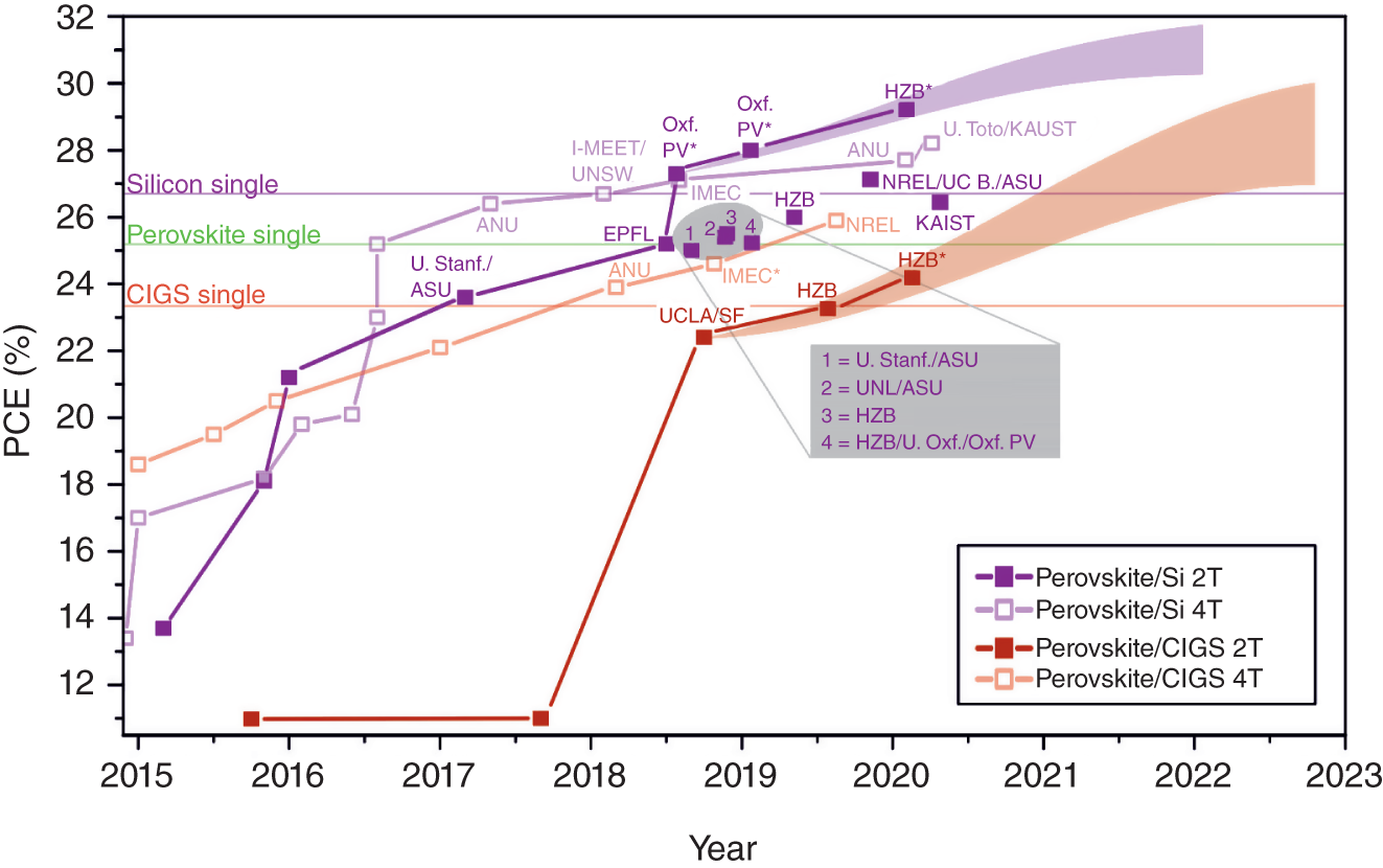
Figure 17.10 Efficiency evolution for perovskite‐based tandem solar cells in two‐terminal (2T) and four‐terminal (4T) configuration with Silicon (Si) or Cu(In,Ga)Se2 (CIGS) bottom cells until mid 2020. Data are extracted from press releases (marked with *) or published papers and the abbreviation indicates the company or university/institute reporting the value. The colored areas indicate a possible efficiency evolution scenario for perovskite‐based 2T tandems with CIGS (red) and silicon (purple).
Source: Based on Bush et al. [41].
As discussed earlier, for 2T tandem cells both subcells are connected in series and the electrical connection between them is formed by a p/n tunnel or recombination junction. These recombination junctions are either formed by highly doped silicon layers [42] or by degenerately (very highly) doped transparent conductive oxides such as indium tin oxide (ITO) [49]. In each of the two subcells, one electron‐hole pair is generated. One of the two charge carriers can be extracted through the external contact of this subcell – an electron leaving through the “negative” terminal of the 2T tandem cell and the hole recombining with an external electron at the “positive” contact. The other two charge carriers must recombine at the junction of the two sub cells to provide overall charge neutrality. In other words, one electron is entering the tandem cell via the “positive” terminal, gains a voltage in the first sub cell, changes into the other sub cell via the recombination junction (losing a bit of its energy), gains more voltage in the second sub cell and leaves the solar cell at the “negative” terminal.
Table 17.1 Latest results for perovskite/silicon tandem solar cells with 2T or 4T configurations.
| References | Abbreviations used in Figure 17.10 | Published (Y/M) | Area (cm2) | JSC (mA/cm2) | FF (%) | Voc (V) | PCE (%) | MPP (%) | Eg Pero (eV) |
|---|---|---|---|---|---|---|---|---|---|
| 2T perovskite/silicon | |||||||||
| Recent efficiency evolution with silicon heterojunction bottom cells | |||||||||
| Sahli [42] | EPFL | 2018/06 | 1.42 | 19.5 | 73.2 | 1.79 | 25.5 | 25.2a) | 1.60 |
| Bush [43] | U. Stanf/ASU | 2018/08 | 1.0 | 18.4 | 77 | 1.77 | 25.0 | 1.63 | |
| Chen [44] | UNL/ASU | 2019/01 | 0.42 | 17.8 | 79.4 | 1.80 | 25.4 | 1.64 | |
| Jošt [45] | HZB | 2018/10 | 0.77 | 18.5 | 78.5 | 1.76 | 25.5 | 1.63 | |
| Mazzarella [46] | HZB/U.Oxf./Ox PV | 2019/02 | 1.10 | 19.0 | 74.6 | 1.79 | 25.4 | 25.2a) | 1.63 |
| Köhnen [47] | HZB | 2019/05 | 0.77 | 19.2 | 76.6 | 1.77 | 26.0 | 26.0 | 1.63 |
| Oxford PV [48] | Ox PVb) | 2018/12 | 1.03 | 19.8 | 78.7 | 1.80 | 28.0a) | — | |
| Xu/Boyd [49] | NREL/UC.B./ASU | 2020/03 | 1.0 | 19.1 | 75.3 | 1.89 | 27.13 | 27.04 | 1.67 |
| Al‐Ashouri/Köhnen [50] | HZBb) | 2020/01 | 1.06 | 19.2 | 79.4 | 1.90 | 29.15a) | 1.68 | |
| Kim [51] | KAIST | 2020/04 | 1.00 | 18.8 | 76.4 | 1.82 | 26.20a) | 1.68 | |
| Results on fully textured bottom cells | |||||||||
| Sahli [42] | EPFL | 2018/06 | 1.42 | 19.5 | 73.2 | 1.79 | 25.5 | 25.2a) | 1.60 |
| Nogay [52] | 2019/03 | 1.42 | 19.5 | 74.7 | 1.74 | 25.4 | 25.1 | — | |
| Lamanna [53] | 2020/02 | 1.43 | 18.8 | 77.5 | 1.80 | 26.3 | 25.9 | 1.64 | |
| Chen [54] | 2020/01 | 0.42 | 19.2 | 74.4 | 1.82 | 26.2 | 26.1 | 1.65b) | |
| Hou/Aydin [55] | 2020/03 | 0.83 | 19.1 | 73.4 | 1.79 | 25.7a) | 1.68 | ||
| Results on non‐silicon‐heterojunction bottom cells | |||||||||
| Wu [56] | 2017/10 | 1 | 17.6 | 73.8 | 1.75 | 22.8 | 22.5 | 1.62 | |
| Zheng [57] | 2018/10 | 16 | 16.2 | 78 | 1.74 | 21.9 | 21.8 | 1.58 | |
| Shen [58] | 2018/12 | 1 | 17.8 | 78.1 | 1.76 | 24.5 | 24.1 | 1.63 | |
| Zheng [59] | 2019/10 | 4 | 16.5 | 81.0 | 1.73 | 23.1 | 23.0 | 1.61 | |
| References | Abbreviations used in Figure 17.10 | Published (Y/M) | Areas (cm2) | JSC (mA/cm2) | FF (%) | Voc (V) | PCE (%) | Combined (%) | |
| 4T perovskite/silicond) | |||||||||
| Recent efficiency evolution | |||||||||
| Duong [35] | ANU | 2017/04 | 0.3/4 | 19.4/18.8 | 70/80 | 1.13/0.69 | 16.0/10.4 | 26.4 | 1.73 |
| Ramírez Quiroz [60] | i‐MEET/UNSW | 2018/01 | 0.1/1 | 21.0/17.7 | 74/80 | 1.10/0.67 | 17.1/9.6 | 26.7 | 1.57 |
| Jaysankar [61] | IMEC | 2018/12 | 0.13/4 | 15.4/24.1 | 73/81 | 1.22/0.68 | 13.8/13.3 | 27.1 | 1.72 |
| Duong [62] | ANU | 2020/01 | 0.21/4 | 18.0/19.6 | 78/78 | 1.2/0.69 | 17.1/10.7 | 27.7 | 1.72 |
| Duong [62] | 2020/01 | 1/1 | 17.5/18.6 | 76/80 | 1.2/0.68 | 16.1/10.7 | 26.2 | 1.72 | |
| Chen [63] | U. Toronto/KAUST | 2020/03 | 0.05/3 | 22.3/17.2 | 78/77 | 1.12/0.7 | 19.0/9.2 | 28.2 | 1.63 |
2T monolithic solar cells are listed in three different categories: (i) recent efficiency evolution with mostly silicon‐heterojunction bottom cells which is so far the major design route in terms of publication number, (ii) results on fully textured wafers and (iii) results on other (non‐silicon‐heterojunction) bottom cells.
a Certified values.
b Values taken from press releases.
c Value for band‐gap taken from PL emission maximum.
d For 4T results, the first value refers to the perovskite top cell and the second value to the silicon bottom cell.
Table 17.2 Results of notable perovskite/CIGS tandem solar cells.
Source: Based on Han et al. [64].
| References | Abbreviations used in Figure 17.10 | Published (Y/M) | Area (cm2) | JSC (mA/cm2) | FF (%) | Voc (V) | PCE (%) | MPP (%) | Eg Pero (eV) |
|---|---|---|---|---|---|---|---|---|---|
| 2T perovskite/CIGS | |||||||||
| Han [64] | UCLA/SF | 2018/08 | 0.04 | 17.3 | 73 | 1.77 | 22.43a) | 1.59 | |
| Jost [65] | 2019/01 | 0.8 | 18.0 | 76 | 1.58 | 21.6 | 21.6 | 1.63 | |
| Al‐Ashouri [66] | HZB | 2019/10 | 1.04 | 19.2 | 72 | 1.68 | 23.26a) | 1.63 | |
| HZB [67] | HZBb) | 2020/01 | 1.05 | 18.8 | 72 | 1.77 | 24.16a) | 1.68 | |
| References | Abbreviations used in Figure 17.10 | Published (Y/M) | Areas (cm2) | JSC (mA/cm2) | FF (%) | Voc (V) | PCE (%) | Combined (%) | |
| 4T perovskite/CIGSc) | |||||||||
| Shen [68] | ANU | 2018/01 | 0.3/0.5 | 22.2/13 | 70/0.72 | 1.13/0.62 | 18.1/5.8 | 23.9 | 1.62 |
| IMEC [69] | IMECb) | 2018/09 | 24.6 | 1.72 | |||||
| Hoe Kim [70] | NREL | 2019/07 | 0.06/0.42 | 19.6/15.6 | 77/79 | 1.13/0.71 | 17.1/8.8 | 25.9 | 1.68 |
Certified values are labeled witha), first value refers to perovskite top cell, second value to CIGS bottom cell.
a) Certified values.
b) Values taken from press releases.
c) For 4T results, the first value refers to the perovskite top cell and the second value to the CIGS bottom cell.
The scenario is also illustrated in Figure 17.5b. In order to enable the sketched scenario without significant losses, the recombination layer must provide the following three main properties: (i) very good selectivity for the respective charge carriers, (ii) favorable energetic alignment for lossless photo‐voltage addition, and (iii) low series resistance. Furthermore, it must also provide high optical transparency for the bottom‐cell response in the near infrared (NIR) region.
As for all solar cells, the absorption of the incident sunlight can be improved using various light management techniques [71, 72]. Especially for 2T tandem solar cells current matching at highest possible values is of utmost importance. First, measures to increase the in‐coupling of light into the solar cell, which is to reduce the reflective losses at the front side, and secondly light trapping techniques, which aim to increase the absorption in the absorber layer usually with textures that scatter the incident light and hence lead to an increase of the average path length of the light in the absorber. Textures or nanotextures also can be used for better in‐coupling, however here also planar antireflective layers or layer stacks can be used. In tandem solar cells, the optics of intermediate layers in‐between the top and bottom cells can be used to redistribute and light between top and bottom cells [46, 72].
In Sections 17.5.1 and 17.5.2, we discuss the developments in engineering and improved scientific understanding for perovskite/silicon and perovskite/CIGS tandem solar cells, respectively.
17.5.1 Perovskite/Silicon Tandem Solar Cells
Crystalline silicon photovoltaics is the leading technology in the global PV market, with 95% market share from total module production in 2018 [9]. Therefore, out of the different possible bottom cell technologies for perovskite‐based tandem solar cells, silicon receives by far the highest attention resembling in the highest tandem efficiency realized so far and the highest number of published reports, as shown in Table 17.1 and Figure 17.10. Most silicon solar cells consist of a diffused homojunction and an aluminium back surface field (Al BSF) for enhanced charge extraction. In the improved passivated emitter rear contact (PERC) design, most of the back‐side contact is passivated with a dielectric, such as silicon oxide and or silicon nitride, to reduce surface recombination losses. Only local electrical contacts are formed. For PERC cells, efficiencies up to 24% in commercial wafer size are reported [73]. For passivated emitter and rear locally diffused (PERL) cells with passivated emitter and rear locally diffused design, the long‐time efficiency record has been 25.0% [74]. Single‐junction silicon solar cells with even higher PCE values can be fabricated by implementing full‐area contacts, which are both passivating and selective. One example for such contacts are ultrathin silicon oxides, which are combined with doped polycrystalline layers. Devices with such layers are called polycrystalline silicon on oxide (POLO) or TOPCon and they have demonstrated efficiencies up to 26.1% (with interdigitated back contact [IBC] contacts) [75] and 25.8% (with double sided contacts) [76], respectively. Another concept are silicon heterojunction (SHJ) solar cells, where two ultrathin intrinsic and doped hydrogenated amorphous silicon (a‐Si;H) layers are deposited onto both sides of the solar cell. SHJ cells reach the highest efficiencies for silicon single cells of 25.1% and 26.7% for double sided [77] and IBC [78] contacts schemes, respectively. For further reading on high efficiency silicon single junction solar cells, we refer to reviews by Battaglia et al. [79] and Hermle et al. [80].
In this section, we present the development of perovskite/silicon tandem solar cells until mid 2020; first for 2T monolithic and then for 4T architectures. The 2T tandem section includes a summary of the efficiency improvement, the development of certain device structures such as the bottom and top cell design and electrode polarities as well as implementation of textured surfaces and light management strategies. The main focus here is directed towards the majority of reported results for perovskite/silicon tandem cells that are shown in purple color in Figure 17.10 with rather similar device design being described in Figure 17.11 and the corresponding performance data also found in Table 17.1. In addition, we highlight results on textured wafers and other (non‐silicon‐heterojunction) bottom cells, both categories are also listed in Table 17.1. For more information on the efficiency evolution of perovskite/silicon tandem solar cells, we refer the reader to several review papers by Werner et al. [81], Tai et al. [82], Torabi et al. [83] or, most recently, by Song et al. [84], Hu et al. [85], Jost et al. [31], and the progress report by Shen et al. [86].
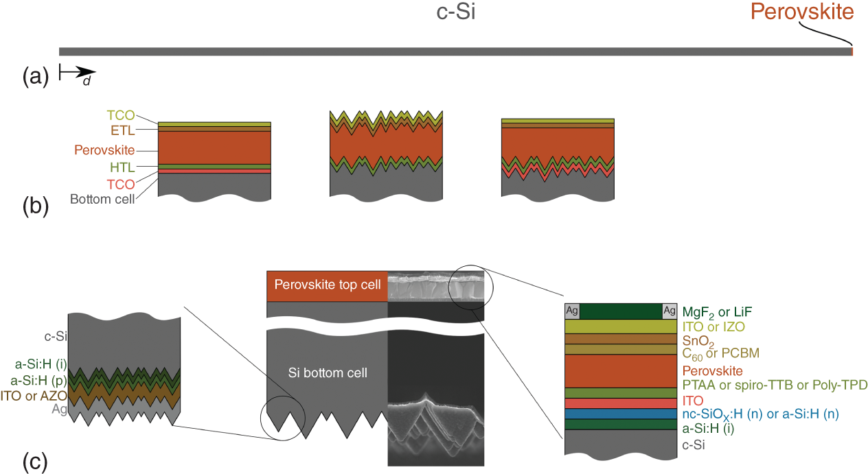
Figure 17.11 Schematic depiction of the 2T perovskite/silicon tandem device architecture: (a) size comparison of the bottom and top cell assuming a wafer thickness of 250 μm and a 500 nm thick top cell; (b) the front side texture and respectively the top cell processing options, reported so far (see Table 17.1, section results on fully textured bottom cells); (c) specific device design and layer stack utilized for most reports in Table 17.1 that enable highest PCE values well above 25%, SEM images and a zoom‐in to top and bottom cell layers are shown as well.
The first perovskite/silicon 2T tandem solar cell was realized on a silicon homojunction bottom cell processed with classical high temperature diffusion process [39]. The tandem cell reached a PCE of 13.7%, strongly limited by its low JSC of 11.5 mA/cm2 which was limited by the highly absorptive, doped Spiro‐OMeTAD film present in the front contact stack. Thus, the overall parasitic absorption equivalent to a loss in photogeneration current density was over 8 mA/cm2 strongly limiting the PCE.
Since then, many researchers focused on SHJ solar cells as bottom cells. The advantage of these cells is their high efficiency, which is reached because of very high Voc values with records up to 750 mV [87]. In addition, the optical loss arising from the front side selective contact made from a‐Si:H does not limit tandem cell operation, because this fraction of the incident light is already absorbed by the perovskite top cell. Besides the high efficiency, typical SHJ cells already feature a TCO, which fully covers the front side. This TCO layer can serve as the bottom contact for the perovskite top cell, just as in single‐junction perovskite solar cells fabricated on glass. This allows relatively simple process integration. Another aspect is the flexibility of the polarity that is offered by the use of SHJ: the bottom cells can be utilized with both polarities and such also the polarity of the perovskite top‐cell can be selected as well which was a key step toward >25% for perovskite/silicon tandem cells, as described below.
The first 2T perovskite/SHJ tandem solar cell was demonstrated in 2015 by Albrecht et al. [88] with 19.9% JV‐scan efficiency and – due to hysteresis – 18.1% efficiency from stabilized MPP‐tracks efficiency, as introduced in Chapter 16. The SHJ utilized as bottom cell was made from an n‐type, double‐side polished float zone (FZ) c‐Si wafer with a front emitter fabricated from thin layers of intrinsic and p‐doped hydrogenated amorphous silicon (a‐Si:H). The p/n recombination junction interconnecting the two sub‐cells was formed between the p‐doped (p)a‐Si:H film and a layer of ITO. ITO is a well‐established electrode material for perovskite single‐junction cells. The perovskite cell was then processed at temperatures below 120 °C in order to avoid degradation of the SHJ cell: The ITO was covered by an atomic layer deposition (ALD)‐processed SnOx film, to form the electronic contact of the perovskite sub‐cell. The FAMAPbI3 perovskite absorber (Eg ∼ 1.57 eV) was 600 nm thick being processed by spin‐coating. The hole selective contact and top contact stack was Spiro‐OMeTAD and thermally evaporated MoOx buffer combined with sputtered ITO. Finally, a LiF film was evaporated on top of the front ITO layer as an antireflective coating. Later that year, Werner et al. showed a strongly improved efficiency in a similar device [89]: They used an almost identical SHJ cell, but with slightly different TCOs and another electron selective (fullerene C60 instead of ALD SnO2) contact for the perovskite top cell to reach a PCE from MPP tracks of 21.2%.
The three papers discussed above are plotted as the first three unlabeled dark purple datapoints in Figure 17.10. In 2017, a key achievement toward higher efficiencies followed by Bush et al. [41]: they switched the tandem polarity from n‐i‐p top cells with front‐emitter SHJ bottom cells to rear‐junction SHJ and p‐i‐n top cells. With that, the parasitic absorption in the n‐type front contact layer stack could be reduced significantly by thinner and less absorbing films. This inverted design has been used ever since and resulted in most of the results summarized in Table 17.1 exceeding 25% PCE.
The above‐mentioned tandem design with rear‐junction SHJ and p‐i‐n perovskite top cells utilized for most tandem reports with efficiency above 25% from Table 17.1 is schematically represented in Figure 17.11. Figure 17.11c displays the general monolithic 2T tandem design with a zoom into the back side and the top cell. Typically, the SHJ back side is fabricated on textured wafers by passivating the wafer with intrinsic (i)a‐Si:H, utilizing (p)a‐Si:H as selective contact and implementing a low absorptive TCO such as ITO or aluminium‐doped zinc oxide (AZO) between the selective contact and the reflecting silver (Ag) back electrode contact. Some tandem designs use silica nanoparticles between the TCO and silver layers to enhance the NIR absorption in the bottom cell and leave approximately 5% of the area uncovered for direct electrical contact between the TCO and the Ag [41, 54]. On the planar (or polished) front side, (i)a‐Si:H forms the passivated, selective contact together with n‐doped (n)a‐Si:H [42] or (n)nc‐SiOx:H [46, 47] and the subcells are interconnected by TCOs such as ITO or tunnel junctions formed by doped silicon layers [47, 52]. The hole‐selective contact of the perovskite top cells is typically formed by organic molecules such as Spiro‐TTB or polymers such as poly(triaryl amine) (PTAA) [42, 49] and the perovskite is processed on top. Spin coating is still used for most of the reported perovskite absorbers in the tandems with compositions such as the “triple cation” FAMACsPb(IxBr1−x)3 or double cations such FACs(IxBr1−x)3. Band gaps of these compositions utilized so far range from 1.63 to 1.68 eV and a constant increase in band gap toward 1.68 eV was found in the development of 2T perovskite/SHJ tandems as shown in Table 17.1. The semitransparent n‐type top cell stack is typically formed by fullerenes or derivatives such as C60 or phenyl‐C61‐butyric acid methyl ester (PCBM), ALD SnO2 as buffer layer, TCOs sputtered at low temperature such as ITO or indium zinc oxide (IZO) and anti‐reflection coating such as LiF or MgF2. Metal fingers or grids are typically made from evaporated Ag. This tandem layer design and material stack enabled reported PCEs up to 29.15% [50]. Future improvements might be possible – next to the optical optimization – by reduction of non‐radiative recombination for these perovskite top‐cells (see also Figure 17.9) in order to improve the top cell Voc and fill factor (FF) and with that the tandem PCE. In addition, Figure 17.11b also visualizes the yet reported strategies to cover textured silicon wafers by either complete conformal coverage [42, 52] or utilization of thick absorber layers in combination with mild textures to fully cover the texture height. Both being explained in more detail below. Figure 17.11 also includes in (a) a scale bar to highlight the size difference between the bottom and top cells.
Usually, single‐junction silicon solar cells are made from textured silicon wafers to effectively reduce reflection and to extend the light path within the absorber layer (light trapping). If light trapping happens via the rear side of the silicon bottom cell only, the perovskite top cell can be processed on the flat front side of the Si wafer without constraints. Therefore, standard texturing processes can be used on the silicon rear side, and indeed, most of today's high efficiency perovskite/SHJ tandem cells are processed on rear side textured wafers with beneficial light trapping in the NIR – data are presented in Table 17.1. Optical simulations, which are briefly discussed in Section 17.6.2, can help to estimate the effect of different light‐trapping measures. The optical simulation studies by Jošt et al. [90] and Santbergen et al. [91] of 2T perovskite/SHJ tandems with such a random pyramid textured rear side showed a gain around ∼0.7 mA/cm2, if a rear side texture is present, which was also demonstrated experimentally by Werner et al. [92]. For reducing reflective losses, the front side has to be textured as well. Jost et al. carried out sophisticated optical simulations of perovskite/SHJ tandems on flat, rear side and both side textured silicon wafers, also considering an optimization of the perovskite band gap [45]. They find a difference of ∼0.5 mA/cm2 in photocurrent density between optimized rear side texture and a double side textured cells, which can result in 1% absolute efficiency gain. For monocrystalline silicon, random pyramid textures with a height and base length of a few micrometers are typically used [42]. However, such feature sizes are incompatible with spin‐coating, which is typically applied for high efficiency lab‐based solar cells. Here, typical thicknesses of around 500 nm and well below 100 nm for the absorber and charge selective layers are utilized, respectively. Therefore, usually additional chemical and/or mechanical polishing is required to planarize the Si surface and enable perovskite spin coating atop [42].
Despite the potential advantages not only in optical properties, but also in terms of process compatibility to standard silicon cell technology, only few results on implementing perovskite cells on bottom cells with random pyramid textures on both wafer sides are reported. As illustrated in Figure 17.11b, 2T perovskite/silicon tandem solar cells with front side textures can be implemented in two ways: (i) a fully conformal deposition of the top cell layers or (ii) utilizing a mild texture and a thick perovskite absorber to fully cover the texture height with the perovskite absorber layer. The first strategy of fully conformal coverage was realized by Sahli et al. in 2018 [42]: To achieve a conformal coating of the perovskite film, they used a hybrid process consisting of first co‐evaporating the inorganic precursor species PbI2 and CsBr to form a porous but conformal film on the texture. Then, this film was infiltrated by a spin‐coated solution of FAI and FABr perovskite precursors and annealed at 150 °C to form the CsxFA1−xPb(I,Br)3 perovskite film. Interestingly, spin coating the organic components on top of the textured and conformally covered (with PbI2 and CsBr) wafer yielded a conformal perovskite film. The final tandem cell has a certified MPP‐tracked PCE of 25.2%. Indeed, the reflection losses are minimal between 400 and 1100 nm and the external quantum efficiency (EQE) of the fully textured tandem reported by Nogay et al. shows low parasitic losses as well as a good current matching between the sub‐cells [52]. The later strategy of utilizing a thick absorber to fully cover the texture height one is reported by Chen et al. [54] and Hou et al. [55]: utilizing a mild sub‐micron to micron texture and a thick perovskite absorber from blade‐ or spin‐coating enabled the complete coverage of perovskite films that showed a rather planarized perovskite top surface on top of the textured silicon wafer. Remarkable monolithic tandem cell efficiencies of 25.7% and 26.1% were realized by the teams of Chen and Hou/Aydin, respectively. Another interesting approach is mechanical stacking into 2T monolithically tandem designs as shown by Ramirez Quiroz et al. [78] andLamanna et al. [53]. Ramirez Quiroz et al. used a planar bottom cell and a conductive adhesive to mechanically and electrical connect both sub cells realizing remarkable fill factors above 80% [78]. Lamanna et al. utilized a fully textured bottom cell by contacting the back electrode of the perovskite top cell with the texturized and metalized front contact of the silicon bottom cell [53]. As of July 2020, the utilization of front side texturing has not enabled highest photocurrents compared to front side flat wafers (compare e.g. the results by Köhnen et al. [47] and Sahli et al. [42]), but it was shown that double side textured wafers, i.e. the standard in silicon PV manufacturing, can be utilized for highly efficient tandems as well and that these could have a better optical efficiency limit.
The first silicon/perovskite tandem solar cell based on an n‐type Si homojunction bottom cell with a standard diffused junction was built by Mailoa and coworkers in 2015 [39]. Soon after, Werner et al. demonstrated 16.3% efficient cells using ZnSnO as recombination layer, a stack of sputtered, compact TiO2 and mesoporous TiO2 as electron transport layer (ETL), and MAPbI3 as top cell absorber [93]. Just as in the cell by Mailoa, they used Spiro‐OMeTAD as hole‐selective layer, which suffered from parasitic absorption at wavelengths shorter than 400 nm limiting the photocurrent density. In 2017, We and coworkers manufactured a tandem cell with a silicon homojunction bottom cell featuring passivating Al2O3 and SiNx films with local contact openings and Cr/Pd/Ag point contacts, covered on the front with an ITO electrode; hence their passivation/point contact schemes was very similar to those in industrial PERC/passivated emitter rear totally diffused (PERT) Si cells. The top cell was similar to Werner's device; the PCE was 22.5% [56]. In 2018, Zheng et al. built tandem solar cells with 16 cm2 device area with an interconnecting layer of SnO2 processed by spin coating from a colloidal precursor and annealing at 150 °C. For this device, a reverse scan PCE of 17.6% and an MPP‐tracked PCE of 17.1% were demonstrated, whereas on 4 cm2 a PCE of 21.0% under reverse scanning and a stabilized PCE of 20.5% was shown [94]. Later that year, the same group demonstrated a 16 cm2 cell with 21.8% PCE; here (FAPbI3)0.83(MAPbBr3)0.17 was used as perovskite [57]. Shen and coworkers applied a different approach by implementing an interconnecting layer stack consisting of ∼54 nm ALD‐grown compact TiO2, followed by a mesoporous TiO2 layer, on two different high‐temperature processed front p/n junctions. Their n‐type c‐Si cells had either a diffused front (p+/n)c‐Si homojunction, or a (p+)polysilicon/silicon oxide/(n)c‐Si passivated front junction (being called POLO or TOPCon contact). The perovskite composition in the top cell was CsRbFAMAPbI3−xBrx with 1.63 eV bandgap and the front contact was a Spiro‐OMeTAD/MoOx buffer/sputtered ITO stack. With an additional antireflection foil, the 1 cm2 cell with passivated polysilicon contact reached an MPP‐tracked efficiency of 24.1% whereas the homojunction‐based tandem had a PCE of 22.9% [58]. In 2019, Zheng et al. presented a 2T perovskite/silicon‐homojunction tandem solar cell with 23.0% MPP efficiency on a 4 cm2 cell. It incorporated a down‐shifting phosphor in the polydimethylsiloxan (PDMS) antireflective film, which absorbs UV photons and re‐emitting green light leading to a small improvement of the integrated photocurrent improvement in external quantum efficiency spectra of around 0.3 mA/cm2 [59].
In 4T perovskite/silicon tandem cells both subcells are processed individually and mechanically stacked on top of each other. A selection of relevant results is listed at the end of Table 17.1. We summarize here the latest developments in efficiency improvements only. 4T tandem cells suffer from less restrictions on the layer integration and enjoy more freedom toward the perovskite top cell design than 2T cells. Free choice of polarity and layer arrangement (substrate vs. superstrate) enabled a continuous efficiency improvement but also more spread and diverse device designs. This can also be seen by the various perovskite top cell band gaps utilized for recent high efficiency designs ranging from 1.57 to 1.72 eV. Typically, the active layer sizes are not matched for the bottom and top cells; Table 17.1 therefore lists the areas of both cells. For unmatched areas the small semitransparent top cell is measured first and then a larger top cell‐like device with similar optical properties (smaller devices have reduced losses from serial losses) is used as a filter for the measurement of the larger bottom cell (due to the rather large diffusion length in crystalline silicon, the bottom cell suffers from edge effects at smaller active areas).
The first report on 4T perovskite/silicon tandem cells with efficiency close to the best silicon single junction was presented by Duong et al. in 2017 [35]. Using a “quadruple” cation composition with MA, FA, Cs, and Rb stabilized the top cell absorber at 1.73 eV bandgap and therefore enhanced efficiency, and reduced both hysteresis and degradation under operation. The mesoporous top cell with PTAA instead of Spiro‐OMeTAD as hole‐transporting layer had an enhanced NIR transmission and allowed to realize a 26.4% tandem solar cell. In early 2018, Ramirez Quiroz et al. achieved a tandem efficiency of 26.7% using a planar p‐i‐n top cell with a CH3NH3PbI3 absorber (1.57 eV bandgap) and silver nanowires as transparent top contact [60]. In late 2018, Jaysankar et al. improved the 4T tandem further by using a CsFAPbIBr perovskite composition with 1.72 eV band gap [61]. Further, they passivated the perovskite surface by a sub‐nm layer of atomic‐layer‐deposited Al2O3 to further enhance the open‐circuit voltage of the top cell. Combining this planar n‐i‐p top cell with an IBC silicon bottom cell, a PCE of 27.1% was reached. In early 2020, Duong and coworkers achieved a new efficiency record of 27.7% tandem efficiency with a size‐unmatched IBC bottom cell and 26.2% for 1 cm2 size‐matched cell using a PERL bottom cell [62]. They improved their mesoporous n‐i‐p cell by passivating the surface of the quadruple cation perovskite with a large cation n‐butylammonium bromide to enhance both the Voc and also slightly the FF. As of July 2020, the highest 4T tandem efficiency combining perovskite and silicon is 28.2% and was reached using a triple cation perovskite composition with 1.63 eV band gap [63]. They used urea as additive to the perovskite, which enhanced the carrier diffusion length and therefore allowed to increase the perovskite thickness, leading to increased absorption and an unprecedented photocurrent density exceeding 22 mA/cm2 in the semitransparent top cell and 39.5 mA/cm2 in the 4T tandem.
After discussing the efficiency and device‐development of 2T and 4T perovskite/silicon tandem solar cells, we now will briefly look at more practical properties such as operational stability and upscaling toward larger. To evaluate the operational stability, long‐term MPP tracking is used and the most stable perovskite single cells reach T80 stabilities (the time when they are degraded to 80% of the initial performance) of >1000 hours [95, 96]. The stability under MPP tracking depends on the measurement conditions, such as device temperature, spectral illumination condition such as with or without UV irradiation, and the atmospheric conditions such as oxygen and moisture levels. As good practice, writing these conditions directly into the MPP tracking figures has evolved. However, long‐term MPP tracking of tandem solar cells is only rarely reported in the literature and yet non‐standardized. Tandem devices without encapsulation were tested in ambient conditions and retained 90% after 61 hours [42] and 92% after 100 hours [54], as reported by Sahli and Chen, respectively. Encapsulated tandem devices on the other hand by Hou et al. were light‐soaked under 400 hours MPP load at 40 °C but showed no degradation [55].
In 2019, Kamino et al. reported on a perovskite/SHJ tandem cell with 57.4 cm2 aperture area and 22.6% PCE [97]. However, for commercial applications, at least the full wafer formats M2 or better M6 need to be developed, with areas of around 244 and 274 cm2, respectively. The continuous trend toward larger wafers might also force the required area for top cells to M12 format, which is 21 cm × 21 cm = 441 cm2 area. It is very important to demonstrate homogeneous top‐cell layer coverage on this area, which can be potentially achieved by blade coating as used by Chen et al. [54] or vacuum‐based methods [98]. In addition, also low‐temperature curing grids and grip pastes with minimal contact resistance to the TCO need to be developed and implemented. First results on this aspect were reported by Kamino et al. [99]. For further reading, we highlight reviews on large area processing for perovskite single junctions that were e.g. published by Chen et al. [100].
17.5.2 Perovskite‐Chalcogenide Tandem Solar Cells
Besides crystalline silicon, also CIGS [Cu(In,Ga)Se2] or copper indium selenide (CIS) [CuInSe2] are suitable materials for the bottom cells of tandem cells with a perovskite top cell. In 2019, 1.6 GWp of PV modules based on CIGS or CIS were produced, which is around 1.2% of the totally produced PV modules [101]. Because of the direct bandgap of CIGS, the absorbers can be made much thinner than in Si solar cells. Hence, this technology enables low material and energy consumption. In other words, CIGS solar cells are a thin‐film technology and therefore would allow true thin‐film tandem cells, which can be fabricated as light‐weight modules with a high power‐to‐weight ratio, flexibility and radiation hardness for space applications [102]. The bandgap of CIGS can be tuned by varying the In:Ga ratio between ∼1.7 eV for CuGaSe2 and ∼1.0 eV for CuInSe2. Comparing the best CIGS single‐junction cell with 23.25% PCE [103] to the best front‐side‐planar silicon solar cell with 22.1% PCE [104] shows that CIGS might have an obvious advantage.
In this section we discuss the efficiency evolution of 2T and 4T perovskite/CIGS tandems solar cells until mid 2020 and conclude with a short paragraph on stability and upscaling. The number of published reports on perovskite/CIGS tandem solar cells is significantly lower than for perovskite/silicon tandem solar cells, which can be seen by the number of data points in Figure 17.10 and when comparing the numbers of entries in Tables 17.1 and Table 17.2. Only few reports on 2T perovskite/CIGS solar cells have been published. This is likely because of the roughness of the CIGS bottom cell surface, as we will discuss below.
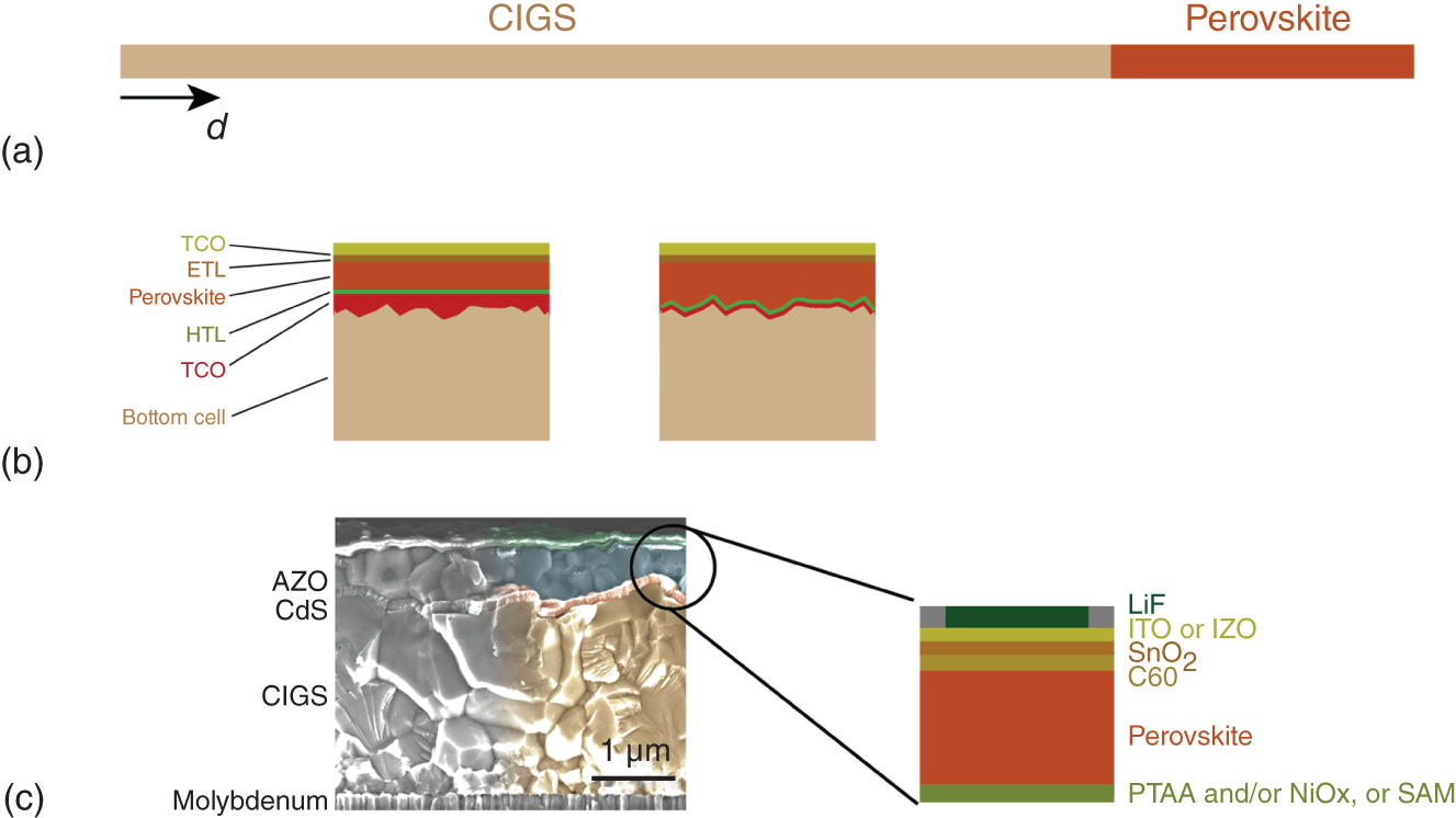
Figure 17.12 Schematic depiction of the 2T perovskite/CIGS tandem device architecture: (a) size comparison of the bottom and top cell assuming a 2–3 μm thick CIGS bottom cell and a 500 nm thick perovskite top cell; (b) the front side texture and respectively the top cell processing options, reported so far; (c) specific device design and layer stack utilized for the few reports in Table Table 17.2, SEM images for top and bottom cell layers are shown as well.
Source: Based on Han et al. [64].
Figure 17.12a shows a thickness comparison of a 2–3 μm thick CIGS bottom cell and a 500 nm thick perovskite top cell. In contrast to wafer‐based silicon tandem solar cells, here a true thin film tandem with an overall thickness below 5 μm can be built. Figure 17.12c shows the typical device structure of CIGS bottom cells: it consists of a substrate, a molybdenum (Mo) back contact, the p‐type CIGS absorber, an n‐type CdS absorber and a zinc oxide (ZnO) front contact. Here, the CIGS and CdS layers form a p–n junction. Due to this defined polarity in the typical substrate configuration, only the p‐i‐n perovskite top cell configuration has been used in 2T tandem devices so far. As a consequence, the top cell designs used for CIGS or SHJ bottom cells were recently merged and p‐i‐n perovskite top cells were implemented in both designs (compare Figures 17.11 and 17.12). Luckily, this restriction is not crucial, because optical losses in a p‐i‐n top cell configuration are much smaller than in n‐i‐p designs, as explained in Section 17.5.1.
Figure 17.12b illustrates two examples of monolithic integration for 2T perovskite/CIGS tandem solar cells by either using polishing of the intermediate TCO (left) or conformal coverage of the charge selective layers (right). Both will be described below. Overall, only a few reports on monolithic perovskite/CIGS tandem solar cells can be found in the literature, with best ones summarized in Table Table 17.2. Reasons for this low number are – amongst others – polarity restrictions and processing restrictions. Most importantly, the deposition of CIGS absorber results in a relatively rough surface, in the range of σRMS = 50–200 nm, with surface features of high aspect ratio [65]. While the typical perovskite absorber thickness of around 500 nm is sufficient to fully cover the rough CIGS surface, high‐performance hole selective layer for the perovskite top cell, commonly deposited via solution processing, cannot cover the rough CIGS surface. This very likely leads to a shunted top cell and makes fabrication of a monolithic perovskite/CIGS tandem very challenging. Consequently, only three reports on 2T perovskite/CIGS cells with efficiencies higher than 20% were published by July 2020; they are summarized in Table Table 17.2.
Todorov et al. reported the first 2T perovskite/CIGS tandem device in 2015 with 11% PCE [40]. This tandem cell was based on a bottom cell being processed from solution instead of typical sputtering or co‐evaporation processes, thus reducing the surface roughness. As a hole selective layer between top and bottom cells a thick poly(3,4‐ethylenedioxythiophene):polystyrene sulfonate (PEDOT:PSS) layer was used, which smoothened the bottom‐cell surface even further. While this layer protected the top cell from shunting, the overall tandem cell performance might have suffered from reduced Voc because of high recombination losses at the PEDOT:PSS/perovskite interface [105] and an ultrathin semitransparent metal front contact.
In 2018, Han and coworkers presented a top‐cell integration, where the front surface is polished to obtain a flat surface [64], similar to what is done for perovskite/silicon tandems. They sputtered a thick ITO recombination layers on top of the CIGS bottom cell and polished it to reduce roughness as shown in Figure 17.12b. With that, the spin‐coating of perovskite and very thin hole selective layers could be implemented. Consequently, a PCE of 20.8% on 0.52 cm2 was obtained and a certified PCE of 22.4% on 0.042 cm2 (see also Table Table 17.2). This tandem shows a high Voc of 1.78 V, which is the highest value reported for this tandem technology, as of July 2020. Because of the thick ITO recombination layer, the free‐carrier absorption increases in the NIR, reducing the generated current density in the bottom CIGS sub‐cell. Thus, the overall tandem JSC of only 17.3 mA/cm2 is rather moderate.
Another approach was reported by Jošt et al. in early 2019: instead of polishing the CIGS cell to obtain a flat surface, they conformally deposited a hole transport layer directly on top of the rough as‐grown CIGS surface [65]. 10 nm of ALD grown NiOx were sufficient to form a conformal, closed layer. In addition, a spin‐coated PTAA polymer layer reduced interface recombination between the conformal NiOx and the perovskite, even though, the polymer itself might not have been covered fully conformal in a dense film, leaving some of the NiOx uncovered. This enabled 21.6% PCE on an area of 0.78 cm2. The current density of this cell was 18.0 mA/cm2 and therefore higher than by Han et al., despite a strong current mismatch between the sub‐cells. This high current density could be achieved by low parasitic absorption in the recombination layer and the rough internal interfaces, which reduced internal reflection. However, this tandem device has a rather low Voc below 1.6 V.
Al‐Ashouri et al. developed the idea of conformally deposited layers even further and used a self‐assembled monolayer (SAM) acting as the hole selective layer [66]. This ultrathin SAM layer binds to oxide surfaces (e.g. ITO, ZnO) and thus connects the tandem recombination contact with the perovskite top‐cell absorber. Despite being only a single molecular layer, the strong binding affinity and self‐assembly ensures closed layers even on rough surfaces. The almost lossless SAM/perovskite interface additionally resulted in an improved Voc, which, combined with improved light management, yielded a certified current record PCE for perovskite/CIGS tandems of 23.3% on more than 1 cm2 area (see also Figure 17.10).
In January 2020, a team from Helmholtz‐Zentrum Berlin (HZB) manufactured a perovskite/CIGS tandem solar cell with a certified efficiency of 24.16% [106]. This result was realized by improving the Voc to the value by Han et al. Based on these results, the future efficiency development is sketched in Figure 17.10. As the efficiency potential for perovskite/CIGS tandem is highly comparable to perovskite/silicon tandems [31], it is assumed that the efficiency will quickly increase to well above 26% for perovskite/CIGS tandem and could ultimately catch up with perovskite/silicon tandems above 30%.
Now we discuss developments on four‐terminal perovskite/CIGS solar cells starting with the first cell that was significantly outperforming the best CIGS single junction: Shen et al. reported in early 2018 a combined tandem efficiency of 23.9% by using a quadruple‐cation perovskite composition with 1.62 eV band gap as also utilized for their 2T perovskite/silicon tandems [58, 68]. In addition, they also report on a MA‐free perovskite compoisiton with 1.75 eV band gap that is characterized by higher stability toward oxygen atmosphere. It is supposed that MA cations and oxygen molecules interact and enhance the surface recombination, which is identified as main driver for oxygen‐induced degradation [68]. A further enhancement toward efficiency was reported by IMEC in September the same year: They improved the NIR transmittance of the perovskite top cell by adding optical coupling layers and by optimizing the transparent electrodes. In addition, the perovskite itself was optimized toward a 1.72 eV band gap which is close to the fundamental optimum for higher tandem efficiency [69]. The latest report with the highest 4T tandem efficiency of 25.9% was announced by Hoe Kim and coworkers: using additives such as the large organic cation phenethylammonium iodide (PEAI) and lead thiocyanate (Pb(SCN)2) improved the perovskite film quality with enhanced crystallinity, reduced formation of excess PbI2, a lower defect density and also higher charge carrier mobility as well as lifetime [70]. This enabled a highly performing perovskite top cell with around 20% and a combined tandem efficiency of 25.9%, the yet highest reported value for any kind of perovskite/CIGS tandem solar cells.
The results in this section highlight the versatile potential of perovskite/CIGS tandem solar cells. Although less results and lower performance was reported in comparison to perovskite/silicon tandems, Jošt et al. recently compared the efficiency potential between silicon and CIGS and found that comparable efficiency metrics above 33% could be achieved [31] with realistic material properties and device designs. Therefore, we forecast a strong efficiency improvement for perovskite/CIGS tandem solar cells toward 30% within the next two to three years.
At the end of this section, we briefly summarize the more practical properties such as operational stability and upscaling toward larger areas for perovskite/CIGS tandems although the number of reports is yet limited. Larger area perovskite mini modules and their integration into tandem devices were reported by Jaysankar et al. [107]. When scaling the semi‐transparent from 0.13 toward 4 cm2 (seven series connected sub cells) and 16 cm2 the efficiency drops from 16.7% to 14.8% and to 12.0%, respectively. Combining the 4 cm2 mini module with a CIGS bottom cell, an area matched tandem efficiency of 21.3% was achieved [107]. For perovskite/CIGS tandems, module integration by series connection of sub‐cells and the deposition on the m2 area are two important challenges toward commercialization. Another important aspect for outdoor tandem modules is operational stability. Long term MPP tracking was reported by Han et al.: non‐encapsulated tandems retained 88% of the initial performance after 500 hours under continuous one‐sun illumination at 30 °C ambient conditions. After storing the tandems in dark for 12 hours, it recovered to 93% of its initial performance [64]. The perovskite‐specific dark recovering might induce higher operational stability under outdoor conditions [108], ensuring high energy yields over a long tandem module operation time scale.
17.6 Energy Yield Calculations
The performance of solar cells is usually measured under standard testing conditions (STC) [12], hence the solar cells are illuminated according to the AM1.5g spectrum [2] with a total radiant power density of 1000 W/m2 at 25 °C.
A tandem solar cell, which outperforms a comparable single‐junction solar cell under STC, does not necessarily perform better than the reference cell under realistic conditions. Especially for monolithic two‐terminal cells, where current matching is required for a high overall photocurrent density, spectral changes may be detrimental to the solar‐cell performance. Further, changes in temperature affect the performance of solar cells. Therefore, STC are often not sufficient for reliably assessing the potential of tandem solar cells.
A better assessment can be achieved by estimating the energy yield (EY), which is the electric energy a photovoltaic system is expected to generate in a given amount of time, often a year. While the performance of a solar cell under STC can be measured in laboratories, the energy yield only can be measured in outdoor testing facilities. In addition, measuring a solar cell in such a facility throughout the course of a year will not directly allow to interpolate the solar cell performance to the future because of variabilities of weather.
Therefore, the energy yield often is assessed using numerical methods. For estimating the annual energy yield, the power P(t) needs to be calculated throughout the year and the power must be integrated over this time. Figure 17.13 shows a schematic flowchart for calculating the power at a given timestamp.

Figure 17.13 Flowchart for calculating the power output of a solar module.
17.6.1 Illumination Model
First, the irradiance onto the module needs to be calculated. It depends, amongst others, on the position of the Sun in the Sky, the direct normal irradiance (DNI) of the sunlight, the diffuse horizontal irradiance (DHI) irradiance of the light from the sky and the orientation of the module. These data are provided by many institutions, such as national weather services or the National Renewable Energy Laboratory (NREL) in the USA. Some sources provide data for many years, here the annual energy yield would be calculated by averaging over several years. Others, such as NREL, provide data for a typical meteorological year (TMY). For tandem solar cells, it is especially relevant to have spectral data, because this determines how the incoming light is distributed between the two subcells. Currently, most databases do not provide these data, however. If no spectral data is available the spectral distribution of the light can also be described by the average photon energy (APE), which for example was used by Futscher and Ehrler [109]. A high APE value corresponds to a blue‐rich spectrum, while a red‐rich spectrum leads to a low APE. While some models consider a singular module with no shadowing effects by other modules [110], other models consider the PV module to be in a large PV field, therefore taking shadowing effects into account [8]. The most complex models also consider the surrounding, including detailed shadowing by buildings at a specific location [111].
17.6.2 Optical Model
When the irradiance is determined, it can be used to calculate the spectral intensity profile throughout the absorber layer Iλ(z), where z is the vertical position within the absorber. A detailed optical model should take all layers of the solar cell into account; it is relevant to know the thickness and the wavelength‐dependent complex refractive index data of every layer. Especially in the quickly evolving field of perovskite solar cells, where material compositions of the different layers change often, this task is very relevant and often requires an individual characterization of the layers in the respective labs. Further, textures of the different surfaces and interfaces in the solar cell strongly affect the optics. Taking them into account in an appropriate manner always increases the simulation time and is not always possible. While large pyramids, which e.g. are commonly present in silicon solar cells can be simulated with approaches such as ray tracing [4, 112], periodic structures with dimensions in the range of the wavelength need rigorous approaches for reliable results, for example the finite elements method [113, 114].
From the intensity profile the absorption in the absorber layer is given by
where d is the thickness of the absorber. If light traverses the absorption layer only once, the intensity decays according to the Lambert–Beer law,
with the absorption coefficient α. However, this relation does not hold if light is reflected from the back into the absorber, if interference is relevant or if the device contains scattering structures.
For a rough estimate, simple optical approaches can be used. For example, every solar cell absorber layer can be assumed to absorb all the light with energies larger or equal then the bandgap: then, all the light reaching the solar cell with energies larger than the top‐cell bandgap is considered to be absorbed there while longer wavelength can reach the bottom cell. In a more realistic but still idealistic approach, the absorption in the weakly absorbing region close to the bandgap can be estimated by the Tiedje–Yablonovitch limit [115] or by an approach by Green [116]. However, these approaches only will yield a layer absorptivity A but no depths‐dependent information.
For detailed electrical simulations, we need the generation rate G(z) (in cm−3), which tells us, how many electron‐hole pairs are generated at depths z. Starting from the spectral intensity Iλ(z), we can obtain the spectral generation rate by
where hc/λ is the photon energy at wavelength λ and ηG is the generation quantum efficiency, usually assumed equal to unity. The generation rate is then obtained via integration

Simpler electrical models or estimates do not require generation profiles, but only the short‐circuit current density. When we assume that every absorbed photon leads to the generation of an electron–hole pair, we obtain the maximum achievable current density,

where Φph, λ denotes the spectral photon flux impinging on the solar modes. For standard optical modeling it is obtained from the AM1.5g spectrum at normal incidence [2]; for detailed energy yield analyses we obtain it from an illumination model as discussed in Section 17.6.1.
Note that the generation rate and the current density need to be calculated for the absorbers in the top cell and the bottom cell.
17.6.3 Electrical Model
The final step in the chain of models sketched in Figure 17.13 is the electrical model. A very rigorous method for electrical modeling is to calculate the depth profiles of the electron concentration n(z) and hole concentration p(z), from which the electrical potentials and hence the band diagram of the device can be calculated, which is the base for the current density – voltage characteristic. All this is explained in detail for example in Reference [6], Chapters 6–8. The calculations are based on three sets of equations:
- The continuity equation ensures the conservation of charge, not only when electrons and holes flow through the solar cell, but also when electron‐hole pairs are generated as described in Section 17.6.2, or when they recombine via recombination mechanisms such as radiative recombination, defect‐driven Shockley‐Read‐Hall recombination or Auger recombination, which is relevant in indirect semiconductors. More information on generation and recombination is for example given in Ref. [6], chapter 7.
- The transport equation relates the current density to gradients in potential and charge density. Here the current density J(z) is driven by diffusion, which is caused by concentration differences of the charge carriers at different positions z in the semiconductor, and by drift due to electric fields.
- The Poisson equation relates the electrical potential and hence the electrical field to the sum of all charge densities.
Using these equations, the electron and hole concentrations across a solar cell can be calculated and the current density – voltage characteristic can be extracted. Usually, these equations cannot be solved analytically but require a numerical approach. Next to commercial programs, several academic groups have developed solvers to study the device physics of solar cells, e.g. [117, 118]. While these programs are well‐suited to simulate single‐junction solar cells, they often have great difficulties in covering the physics happening at the recombination contact of monolithic tandem solar cells, where the top and bottom cells are electrically connected to each other. Further, this kind of simulations is relatively expensive in terms of computational capacity and takes relatively long, which makes them less suited for energy yield analyses, where the simulations must be conducted for many time steps.

Figure 17.14 The equivalent circuit according to the one‐diode model.
A much simpler analytical approach is to electrically describe the solar cell via a one‐diode model, where we consider the solar cell to consist of a photocurrent source Iph, a diode, a parallel (shunt) resistance Rp and a serial resistance Rs, as illustrated in Figure 17.14. Mathematically, the current density – voltage characteristic of this circuit is given by
with the dark current I0, the diode ideality factor m, the unit charge q, the Boltzmann constant k, and the temperature T. For Rs = 0, Rp → ∞, and m = 1 the equation reduces to the Shockley equation 17.3, which describes an ideal diode. We used it in our derivation of tandem solar cell efficiency limits in Section 17.3. For some types of solar cells, such as silicon solar cells, models consisting of a single diode cannot describe the solar‐cell behavior accurately. Then, two‐diode models can be used where two diodes are assumed to be in parallel: one is an ideal diode with ideality factor m = 1, the other one has a different ideality factor (see e.g. Ref. [6], chapter 9): With such models, monolithic two‐terminal solar cells can be modeled as sketched in Figure 17.4b. One‐diode models have been used by several authors for their energy yield analysis of tandem solar cells [110, 119].
Each of the approaches described above leads to a current density – voltage characteristic, for which the MPP needs to be determined. The maximum power can then be used for the energy yield calculation.
In an even simpler approach, the external solar cell parameters of experimentally measured single‐junction solar cells are taken as starting points: the open‐circuit voltage Voc, ref, the short‐circuit current density Jsc, and the fill factor FF. Using optical simulations, a maximum achievable current density Jph is determined for each subcell and taken as new value for Jsc – for monolithic tandem solar cells the lower one of these two photocurrents is also used for the other subcell in order to mimic current matching. Then, the open‐circuit voltage is determined by accounting for the logarithmic relationship between current density and voltage,
Finally, the FF is assumed to stay constant. Assuming this approach, a power density is determined for the two subcells and the two power densities are added. This approach was for example used for layer thickness optimizations of monolithic tandem solar cells [45, 113, 120].
17.6.4 Temperature Model
The electrical performance is not only determined by the irradiance which reaches the solar cell, as described in Section 17.6.1, but also by the solar cell temperature. The temperature affects many electronic processes in the solar cell, such as recombination rates and – as a consequence – the voltage. For detailed energy‐yield analyses and electrical modeling, knowledge of the solar‐cell temperature, which might be significantly hotter than the surface of the solar module, is therefore very important.
The temperature of a solar cell within the solar module is determined by several factors: temperature of the surrounding, irradiance on the module, wind at the module – which is also dependent on the installation height of the module. Some models that can be used to estimate the module temperature are described in Ref. [6], section 20.3.
The effect of temperature on the performance of silicon PV modules is often approximated linearly, where the change per degree Kelvin of a parameter such as the module's PCE, is given as a temperature coefficient. Temperature coefficients are published in datasheets of silicon PV modules. For perovskite solar cells a temperature coefficient of −0.17% per K between 25 °C and 85 °C was published in 2020 [121], which is comparable with silicon solar cells. For perovskite‐based tandem solar cells no temperature coefficients have been determined yet. However, as both perovskite and silicon solar cells show similar temperature coefficients, it is likely that perovskite‐silicon tandem solar cells behave analogously.
17.6.5 Energy Yield Calculation
Above we described the models that are required for an energy yield analysis:
- An illumination model to determine the amount of radiation – and hence the wavelength‐dependent photon flux – hitting the solar module. For tandem modules, where the two cells are susceptible for different wavelength ranges, the illumination model should provide spectral information.
- An optical model that calculates, how much light is absorbed in the absorber layers of the subcells, with the output of the illumination model as input.
- An electrical model, which calculates the current density – voltage characteristic and subsequently the maximum power output at the given illumination and temperature.
- Finally, a temperature model that determines the temperature of the solar module, which is relevant for accurate electrical modeling.
All these models must be performed sequentially for every time step in the period, for which the energy yield should be calculated. Some models described above are very time consuming, such as the finite element method e.g. for optical modeling or numerical electrical models based on the continuity, transport, and Poisson equations. It is not practical to perform them for every time step. Therefore, for energy yield calculations we need to fall back on simpler and faster models. Alternatively, we can use surrogate modeling methods [122], where we perform the rigorous calculations only for a few points. An example for such methods is the reduced basis method [123], which can be applied to the finite elements method [124, 125].
Some authors use energy yield calculations for optimizing different aspects of tandem solar cells, e.g. to study the effect of bandgap and layer stack changes on the performance of 2T‐ and 4T solar cells [119, 126].
17.7 Conclusions and Outlook
In this chapter we have shown that perovskite‐based tandem solar cells with a perovskite top cell and a crystalline silicon or CIGS bottom cell are a very interesting concept because of their high efficiency limits around 45% and more practical limits around 34% for both bottom‐cell materials. Both tandem technologies will break the 30% efficiency barrier within the early 2020s with a sooner breakthrough for perovskite/silicon tandem solar cells. Hence, they offer a huge efficiency potential as compared to any single junction concept.
Both material combinations can be either realized as two‐terminal tandem solar cells, were the two subcells are electrically connected in series or four‐terminal cells, where the two subcells are electrically independent of each other. In addition, also three‐terminal configurations with e.g. interdigitated back contact (IBC) bottom cells become more relevant.
To get closer to the fundamental efficiency limit, more fundamental understanding of the working principle of tandem solar cells, and of the optimal device designs such as two‐, three‐, or four‐terminal configuration is necessary. Therefore both optical and electrical simulations can help to further optimize the designs and choice of materials used for certain charge selective and contact layers.
As of 2020, the major limitations for the two‐terminal devices are engineering problems, such as processing restrictions e.g. the maximum allowed temperature or solvents used, device polarity matching with p‐i‐n or n‐i‐p topcells, and surface texture/roughness of the utilized bottom cells. In addition, also band‐gap optimized perovskite compositions and charge selective contact combinations to enable highest passivation and with that radiative efficiency and open‐circuit voltages. Also, the fill factor of these tandems solar cells lacks behind theoretical predictions. Further optimization of the series resistance losses of the tandem contact design but also more understanding on the internal electrical field distribution might help to improve these parameters further.
In addition, also more practical issues must be considered. Even though scaling toward larger areas already is demonstrated, module integration with typical thin‐film series connection of module sub‐areas and larger area contact design is not yet developed far enough. Further, standard testing protocols for perovskite‐based tandem solar cells need to be defined by the research community, especially accelerated testing protocols under elevated temperature and/or humidity (damp heat) and temperature cycling. In addition, also true outdoor measurements with day/night cycling need to be performed and reported for perovskite‐based tandem solar cells for better comparison.
Looking a decade ahead, also triple‐ and potentially quadruple‐junctions solar cells with perovskite sub‐cells will become more important as they have even higher theoretical efficiency limits than tandems.
In conclusion, multi‐junction solar cells with perovskite subcells are likely to play a crucial role in next‐generation low cost solar modules with efficiencies exceeding 30%.
Acknowledgments
Preparing this chapter would not have been possible without the support of many. First of all, we would like to thank Hiroyuki Fujiwara for giving us the opportunity to contribute to this book with a chapter. Further, we would like to thank Amran Al‐Ashouri, Eike Köhnen and Philipp Tockhorn for supporting us in the preparation of the manuscript. We would like to acknowledge Robert Wenisch, Peter Tillmann and Lars Korte for critically reviewing parts of the manuscript and Christian Kaufmann for providing us with information on CIGS solar cells.
References
- 1 Shockley, W. and Queisser, H.J. (1961). Detailed balance limit of efficiency of p–n junction solar cells. J. Appl. Phys. 32: 510–519.
- 2 A.S.T.M.S. G173‐03 (2008). Standard Tables for Reference Solar Spectral Irradiances: Direct Normal and Hemispherical on 37 Tilted Surface. West Conshohocken, PA: ASTM International.
- 3 K. Jäger, M. Werth, L. Mazzarella, et al. (2017). Numerical optical optimization of perovskite‐silicon tandem solar cells, in 33rd European Photovoltaic Solar Energy Conference and Exhibition. Amsterdam, the Netherlands, 1057–1060 (25–29 September 2017).
- 4 Santbergen, R., Meguro, T., Suezaki, T. et al. (2017). GenPro4 optical model for solar cell simulation and its application to multijunction solar cells. IEEE J. Photovolt. 7: 919–926.
- 5 Rienäcker, M., Warren, E.L., Schnabel, M. et al. (2019). Back‐contacted bottom cells with three terminals: maximizing power extraction from current‐mismatched tandem cells. Prog. Photovoltaics Res. Appl. 27: 410–423.
- 6 Smets, A.H.M., Jäger, K., Isabella, O. et al. (2016). Solar Energy: The Physics and Engineering of Photovoltaic Conversion Technologies and Systems. UIT Cambridge.
- 7 M. Stocks, Y.X. Loo and N.N. Lal (2016). Free the Bandgap! Series‐Parallel Connection of Tandem Cells, in Proceedings of the 32nd European Photovoltaic Solar Energy Conference and Exhibition. Munich, Germany, 223–227 (21–24 June 2016).
- 8 Tillmann, P., Jäger, K., and Becker, C. (2020). Minimising levelised cost of electricity of bifacial solar panel arrays using Bayesian optimisation. Sustain. Energy Fuels 4: 254–264.
- 9 (2019). International Technology Roadmap for Photovoltaic (ITRPV) – 2018 Results, 10e. Frankfurt am Main, Germany: VDMA.
- 10 Guillemoles, J.‐F., Kirchartz, T., Cahen, D., and Rau, U. (2019). Guide for the perplexed to the Shockley–Queisser model for solar cells. Nat. Photonics 13: 501–505.
- 11 Vos, A.D. (1980). Detailed balance limit of the efficiency of tandem solar cells. J. Phys. D: Appl. Phys. 13: 839.
- 12 IEC:60904–3: Photovoltaic devices – Part 3: Measurement principles for terrestrial photovoltaic (PV) solar devices with reference spectral irradiance data, 2008.
- 13 Jia, J., Miao, Y., Kang, Y. et al. (2015). Bias‐dependence of luminescent coupling efficiency in multijunction solar cells. Opt. Express 23: A219.
- 14 M. Mazouchi, J. Jia, Y. Huo, et al. 2015. Luminescent coupling effects in double‐junction solar cells, in 2015 IEEE 42nd Photovoltaic Specialist Conference (PVSC). New Orleans, LA, USA (14–19 June 2015).
- 15 Liu, Z., Krückemeier, L., Krogmeier, B. et al. (2018). Open‐circuit voltages exceeding 1.26 V in planar methylammonium lead iodide perovskite solar cells. ACS Energy Lett. 4: 110–117.
- 16 Ban, M., Zou, Y., Rivett, J.P.H. et al. (2018). Solution‐processed perovskite light emitting diodes with efficiency exceeding 15% through additive‐controlled nanostructure tailoring. Nat. Commun. 9: 9.
- 17 Zou, W., Li, R., Zhang, S. et al. (2018). Minimising efficiency roll‐off in high‐brightness perovskite light‐emitting diodes. Nat. Commun. 9: 2.
- 18 Yang, X., Zhang, X., Deng, J. et al. (2018). Efficient green light‐emitting diodes based on quasi‐two‐dimensional composition and phase engineered perovskite with surface passivation. Nat. Commun. 9: 2.
- 19 Xiao, Z., Kerner, R.A., Zhao, L. et al. (2017). Efficient perovskite light‐emitting diodes featuring nanometre‐sized crystallites. Nat. Photonics 11: 108–115.
- 20 Cho, H., Jeong, S.‐H., Park, M.‐H. et al. (2015). Overcoming the electroluminescence efficiency limitations of perovskite light‐emitting diodes. Science 350: 1222–1225.
- 21 Walker, A.W., Höhn, O., Micha, D.N. et al. (2015). Impact of photon recycling and luminescence coupling on III–V single and dual junction photovoltaic devices. J. Photonics Energy 5: 053087.
- 22 Richter, A., Glunz, S.W., Werner, F. et al. (2012). Improved quantitative description of auger recombination in crystalline silicon. Phys. Rev. B 86 (16): 165202.
- 23 Martí, A. and Araújo, G.L. (1996). Limiting efficiencies for photovoltaic energy conversion in multigap systems. Sol. Energy Mater. Sol. Cells 43: 203–222.
- 24 De Wolf, S., Holovsky, J., Moon, S.‐J. et al. (2014). Organometallic halide perovskites: sharp optical absorption edge and its relation to photovoltaic performance. J. Phys. Chem. Lett. 5: 1035–1039.
- 25 Swartwout, R., Hoerantner, M.T., and Bulović, V. (2019). Scalable deposition methods for large‐area production of perovskite thin films. Energy Environ. Mater. 2: 119–145.
- 26 Albrecht, S. and Rech, B. (2017). Perovskite solar cells: on top of commercial photovoltaics. Nat. Energy 2: 16196.
- 27 Sofia, S.E., Wang, H., Bruno, A. et al. (2020). Roadmap for cost‐effective, commercially‐viable perovskite silicon tandems for the current and future PV market. Sustain. Energy Fuels 2: 852–862.
- 28 Unger, E.L., Kegelmann, L., Suchan, K. et al. (2017). Roadmap and roadblocks for the band gap tunability of metal halide perovskites. J. Mater. Chem. A 5: 11401–11409.
- 29 Gharibzadeh, S., Nejand, B.A., Jakoby, M. et al. (2019). Record open‐circuit voltage wide‐bandgap perovskite solar cells utilizing 2D/3D perovskite heterostructure. Adv. Energy Mater. 9: 1803699.
- 30 Rajagopal, A., Stoddard, R.J., Jo, S.B. et al. (2018). Overcoming the photovoltage plateau in large bandgap perovskite photovoltaics. Nano Lett. 18: 3985–3993.
- 31 Jošt, M., Kegelmann, L., Korte, L., and Albrecht, S. (2020). Monolithic perovskite tandem solar cells: a review of the present status and advanced characterization methods toward 30% efficiency. Adv. Energy Mater. 10: 1904102.
- 32 Zheng, X., Hou, Y., Bao, C. et al. (2020). Managing grains and interfaces via ligand anchoring enables 22.3%‐efficiency inverted perovskite solar cells. Nat. Energy 5: 131–140.
- 33 Zhu, H., Liu, Y., Eickemeyer, F.T. et al. (2020). Tailored amphiphilic molecular mitigators for stable perovskite solar cells with 23.5% efficiency. Adv. Mater. 32: 1907757.
- 34 Hoke, E.T., Slotcavage, D.J., Dohner, E.R. et al. (2015). Reversible photo‐induced trap formation in mixed‐halide hybrid perovskites for photovoltaics. Chem. Sci. 6: 613–617.
- 35 Duong, T., Wu, Y., Shen, H. et al. (2017). Rubidium multication perovskite with optimized bandgap for perovskite‐silicon tandem with over 26% efficiency. Adv. Energy Mater. 7: 1700228.
- 36 Bush, K.A., Frohna, K., Prasanna, R. et al. (2018). Compositional engineering for efficient wide band gap perovskites with improved stability to photoinduced phase segregation. ACS Energy Lett. 3: 428–435.
- 37 Löper, P., Moon, S.‐J., de Nicolas, S.M. et al. (2015). Organic–inorganic halide perovskite/crystalline silicon four‐terminal tandem solar cells. Phys. Chem. Chem. Phys. 17: 1619–1629.
- 38 Bailie, C.D., Christoforo, M.G., Mailoa, J.P. et al. (2015). Semi‐transparent perovskite solar cells for tandems with silicon and CIGS. Energy Environ. Sci. 8: 956–963.
- 39 Mailoa, J.P., Bailie, C.D., Johlin, E.C. et al. (2015). A 2‐terminal perovskite/silicon multijunction solar cell enabled by a silicon tunnel junction. Appl. Phys. Lett. 106: 121105.
- 40 Todorov, T., Gershon, T., Gunawan, O. et al. (2015). Monolithic perovskite‐CIGS tandem solar cells via in situ band gap engineering. Adv. Energy Mater. 5: 1500799.
- 41 Bush, K.A., Palmstrom, A.F., Yu, Z.J. et al. (2017). 23.6%‐efficient monolithic perovskite/silicon tandem solar cells with improved stability. Nat. Energy 2: 17009.
- 42 Sahli, F., Werner, J., Kamino, B.A. et al. (2018). Fully textured monolithic perovskite/silicon tandem solar cells with 25.2% power conversion efficiency. Nat. Mater. 17: 820–826.
- 43 Bush, K.A., Manzoor, S., Frohna, K. et al. (2018). Minimizing current and voltage losses to reach 25% efficient monolithic two‐terminal perovskite–silicon tandem solar cells. ACS Energy Lett. 3: 2173–2180.
- 44 Chen, B., Yu, Z., Liu, K. et al. (2019). Grain engineering for perovskite/silicon monolithic tandem solar cells with efficiency of 25.4%. Joule 3: 177–190.
- 45 Jošt, M., Köhnen, E., Morales‐Vilches, A.B. et al. (2018). Textured interfaces in monolithic perovskite/silicon tandem solar cells: advanced light management for improved efficiency and energy yield. Energy Environ. Sci. 11: 3511–3523.
- 46 Mazzarella, L., Lin, Y.‐H., Kirner, S. et al. (2019). Infrared light management using a nanocrystalline silicon oxide interlayer in monolithic perovskite/silicon heterojunction tandem solar cells with efficiency above 25%. Adv. Energy Mater. 9: 1803241.
- 47 Köhnen, E., Jošt, M., Morales‐Vilches, A.B. et al. (2019). Highly efficient monolithic perovskite silicon tandem solar cells: analyzing the influence of current mismatch on device performance. Sustain. Energy Fuels 3: 1995–2005.
- 48 P.V. Oxford (2018). Oxford PV sets world record for perovskite solar cell. https://www.oxfordpv.com/news/oxford-pv-sets-world-record-perovskite-solar-cell (accessed 28 April 2021).
- 49 Xu, J., Boyd, C.C., Yu, Z.J. et al. (2020). Triple‐halide wide–band gap perovskites with suppressed phase segregation for efficient tandems. Science 367: 1097–1104.
- 50 Al‐Ashouri, A., Köhnen, E., Li, B. et al. (2020). Monolithic perovskite/silicon tandem solar cell with >29% efficiency by enhanced hole extraction. Science 370: 1300–1309.
- 51 Kim, D., Jung, H.J., Park, I.J. et al. (2020). Efficient, stable silicon tandem cells enabled by anion‐engineered wide‐bandgap perovskites. Science 368: 155–160.
- 52 Nogay, G., Sahli, F., Werner, J. et al. (2019). 25.1%‐efficient monolithic perovskite/silicon tandem solar cell based on a p‐type monocrystalline textured silicon wafer and high‐temperature passivating contacts. ACS Energy Lett. 4: 844–845.
- 53 Lamanna, E., Matteocci, F., Calabrò, E. et al. (2020). Mechanically stacked, two‐terminal graphene‐based perovskite/silicon tandem solar cell with efficiency over 26%. Joule 4: 865–881.
- 54 Chen, B., Yu, Z.J., Manzoor, S. et al. (2020). Blade‐coated perovskites on textured silicon for 26%‐efficient monolithic perovskite/silicon tandem solar cells. Joule 4: 850–864.
- 55 Hou, Y., Aydin, E., Bastiani, M.D. et al. (2020). Efficient tandem solar cells with solution‐processed perovskite on textured crystalline silicon. Science 367: 1135–1140.
- 56 Wu, Y., Yan, D., Peng, J. et al. (2017). Monolithic perovskite/silicon‐homojunction tandem solar cell with over 22% efficiency. Energy Environ. Sci. 10: 2472–2479.
- 57 Zheng, J., Mehrvarz, H., Ma, F.‐J. et al. (2018). 21.8% efficient monolithic perovskite/homo‐junction‐silicon tandem solar cell on 16 cm2. ACS Energy Lett. 3: 2299–2300.
- 58 Shen, H., Omelchenko, S.T., Jacobs, D.A. et al. (2018). In situ recombination junction between p‐Si and TiO2 enables high‐efficiency monolithic perovskite/Si tandem cells. Sci. Adv. 4: eaau9711.
- 59 Zheng, J., Mehrvarz, H., Liao, C. et al. (2019). Large‐area 23%‐efficient monolithic perovskite/homojunction‐silicon tandem solar cell with enhanced UV stability using down‐shifting material. ACS Energy Lett. 4: 2623–2631.
- 60 Quiroz, C.O.R., Shen, Y., Salvador, M. et al. (2018). Balancing electrical and optical losses for efficient 4‐terminal Si–perovskite solar cells with solution processed percolation electrodes. J. Mater. Chem. A 6: 3583–3592.
- 61 Jaysankar, M., Raul, B.A.L., Bastos, J. et al. (2019). Minimizing voltage loss in wide‐bandgap perovskites for tandem solar cells. ACS Energy Lett. 4: 259–264.
- 62 Duong, T., Pham, H., Kho, T.C. et al. (2020). High efficiency perovskite‐silicon tandem solar cells: effect of surface coating versus bulk incorporation of 2D perovskite. Adv. Energy Mater.: 1903553.
- 63 Chen, B., Baek, S.‐W., Hou, Y. et al. (2020). Enhanced optical path and electron diffusion length enable high‐efficiency perovskite tandems. Nat. Commun. 11: 3.
- 64 Han, Q., Hsieh, Y.‐T., Meng, L. et al. (2018). High‐performance perovskite/Cu(In,Ga)Se2 monolithic tandem solar cells. Science 361: 904–908.
- 65 Jošt, M., Bertram, T., Koushik, D. et al. (2019). 21.6%‐efficient monolithic perovskite/Cu(In,Ga)Se2 tandem solar cells with thin conformal hole transport layers for integration on rough bottom cell surfaces. ACS Energy Lett. 4: 583–590.
- 66 Al‐Ashouri, A., Magomedov, A., Roß, M. et al. (2019). Conformal monolayer contacts with lossless interfaces for perovskite single junction and monolithic tandem solar cells. Energy Environ. Sci. 12: 3356–3369.
- 67 C. Kaufmann (2020. Highly efficient monolithic 2‐terminal cigse/perovskite tandem solar cells, in Virtual Chalcogenide PV Conference. Berlin, Germany (25–28 May 2020).
- 68 Shen, H., Duong, T., Peng, J. et al. (2018). Mechanically‐stacked perovskite/CIGS tandem solar cells with efficiency of 23.9% and reduced oxygen sensitivity. Energy Environ. Sci. 11: 394–406.
- 69 H. Degans, Perovskite/CIGS tandem cell with record efficiency of 24.6 percent paves the way for flexible solar cells and high‐efficiency building‐integrated PV. https://www.imec-int.com/en/articles/perovskite-cigs-tandem-cell-with-record-efficiency-of-24-6-percent (accessed 28 April 2021).
- 70 Kim, D.H., Muzzillo, C.P., Tong, J. et al. (2019). Bimolecular additives improve wide‐band‐gap perovskites for efficient tandem solar cells with CIGS. Joule 3: 1734–1745.
- 71 Sprafke, A.N. and Wehrspohn, R.B. (2013). Light trapping concepts for photon management in solar cells. GREEN 2: 177–187.
- 72 Lal, N.N., White, T.P., and Catchpole, K.R. (2014). Optics and light trapping for tandem solar cells on silicon. IEEE J. Photovoltaics 4: 1380–1386.
- 73 Chen, R., Tong, H., Zhu, H. et al. (2020). 23.83% efficient mono‐PERC incorporating advanced hydrogenation. Prog. Photovoltaics Res. Appl. 28: 1239–1247.
- 74 Green, M.A., Hishikawa, Y., Dunlop, E.D. et al. (2019). Solar cell efficiency tables (version 53). Prog. Photovoltaics Res. Appl. 27: 3–12.
- 75 Haase, F., Hollemann, C., Schäfer, S. et al. (2018). Laser contact openings for local poly‐Si‐metal contacts enabling 26.1%‐efficient POLO‐IBC solar cells. Sol. Energy Mater. Sol. Cells 186: 184–193.
- 76 A. Richter, J. Benick, F. Feldmann, et al. (2019). Both sides contacted silicon solar cells: options for approaching 26% efficiency, in 36th European Photovoltaic Solar Energy Conference and Exhibition. Marseille, France, 90–95 (9–13 September 2019).
- 77 C. X. Xu (2019). Micro‐crystalline silicon oxide front contact layers for silicon heterojunction solar cells, in 2nd International Workshop on Silicon Heterojunction Solar Cell Technology. Chengdu, China (11–12 November 2019).
- 78 Quiroz, C.O.R., Spyropoulos, G.D., Salvador, M. et al. (2019). Interface molecular engineering for laminated monolithic perovskite/silicon tandem solar cells with 80.4% fill factor. Adv. Funct. Mater. 29: 1901476.
- 79 Battaglia, C., Cuevas, A., and Wolf, S.D. (2016). High‐efficiency crystalline silicon solar cells: status and perspectives. Energy Environ. Sci. 9: 1552–1576.
- 80 Hermle, M., Feldmann, F., Bivour, M. et al. (2020). Passivating contacts and tandem concepts: approaches for the highest silicon‐based solar cell efficiencies. Appl. Phys. Rev. 7: 021305.
- 81 Werner, J., Weng, C.‐H., Walter, A. et al. (2016). Efficient monolithic perovskite/silicon tandem solar cell with cell area >1 cm2. J. Phys. Chem. Lett. 7: 161–166.
- 82 Tai, Q., Tang, K.‐C., and Yan, F. (2019). Recent progress of inorganic perovskite solar cells. Energy Environ. Sci. 12: 2375–2405.
- 83 Torabi, N., Behjat, A., Zhou, Y. et al. (2019). Progress and challenges in perovskite photovoltaics from single‐ to multi‐junction cells. Mater. Today Energy 12: 70–94.
- 84 Song, Z., Chen, C., Li, C. et al. (2019). Wide‐bandgap, low‐bandgap, and tandem perovskite solar cells. Semicond. Sci. Technol. 34: 093001.
- 85 Hu, Y., Song, L., Chen, Y., and Huang, W. (2019). Two‐terminal perovskites tandem solar cells: recent advances and perspectives. Solar RRL 3: 1900080.
- 86 Shen, H., Walter, D., Wu, Y. et al. (2019). Monolithic perovskite/Si tandem solar cells: pathways to over 30% efficiency. Adv. Energy Mater. 10: 1902840.
- 87 Taguchi, M., Yano, A., Tohoda, S. et al. (2014). 24.7% record efficiency HIT solar cell on thin silicon wafer. IEEE J. Photovoltaics 4: 96–99.
- 88 Albrecht, S., Saliba, M., Correa Baena, J.P. et al. (2016). Monolithic perovskite/silicon‐heterojunction tandem solar cells processed at low temperature. Energy Environ. Sci. 9 (1): 81–88.
- 89 Werner, J., Niesen, B., and Ballif, C. (2017). Perovskite/silicon tandem solar cells: marriage of convenience or true love story? – an overview. Adv. Mater. Interfaces 5: 1700731.
- 90 Jošt, M., Albrecht, S., Lipovšek, B. et al. (2016). Back‐ and front‐side texturing for light‐management in perovskite/silicon‐heterojunction tandem solar cells. Energy Procedia 102: 43–48.
- 91 Santbergen, R., Mishima, R., Meguro, T. et al. (2016). Minimizing optical losses in monolithic perovskite/c‐Si tandem solar cells with a flat top cell. Opt. Express 24: A1288–A1299.
- 92 Werner, J., Barraud, L., Walter, A. et al. (2016). Efficient near‐infrared‐transparent perovskite solar cells enabling direct comparison of 4‐terminal and monolithic perovskite/silicon tandem cells. ACS Energy Lett. 1: 474–480.
- 93 Werner, J., Walter, A., Rucavado, E. et al. (2016). Zinc tin oxide as high‐temperature stable recombination layer for mesoscopic perovskite/silicon monolithic tandem solar cells. Appl. Phys. Lett. 109: 233902.
- 94 Zheng, J., Lau, C.F.J., Mehrvarz, H. et al. (2018). Large area efficient interface layer free monolithic perovskite/homo‐junction‐silicon tandem solar cell with over 20% efficiency. Energy Environ. Sci. 11: 2432–2443.
- 95 Wang, Z., Lin, Q., Chmiel, F.P. et al. (2017). Efficient ambient‐air‐stable solar cells with 2D–3D heterostructured butylammonium‐caesium‐formamidinium lead halide perovskites. Nat. Energy 2: 8.
- 96 Lee, J.‐W., Dai, Z., Han, T.‐H. et al. (2018). 2D perovskite stabilized phase‐pure formamidinium perovskite solar cells. Nat. Commun. 9: 8.
- 97 Kamino, B.A., Paviet‐Salomon, B., Moon, S.‐J. et al. (2019). Low‐temperature screen‐printed metallization for the scale‐up of two‐terminal perovskite–silicon tandems. ACS Appl. Energy Mater. 2: 3815–3821.
- 98 Li, J., Wang, H., Chin, X.Y. et al. (2020). Highly efficient thermally co‐evaporated perovskite solar cells and mini‐modules. Joule 4: 1035–1053.
- 99 B. A. Kamino, A. Paracchino, S.‐J. Moon, et al. (2019). Scale‐up technologies towards large area 2‐terminal perovskite‐silicon tandems, in 36th European Photovoltaic Solar Energy Conference and Exhibition. Marseille, France (9–13 September 2019).
- 100 Chen, Y., Zhang, L., Zhang, Y. et al. (2018). Large‐area perovskite solar cells – a review of recent progress and issues. RSC Adv. 8: 10489–10508.
- 101 Burger, B., Kiefer, K., Kost, C. et al. (2020). Photovoltaics Report. Freiburg, Germany: Fraunhofer Institute for Solar Energy Systems ISE.
- 102 Lang, F., Jošt, M., Frohna, K. et al. (2020). Proton radiation hardness of perovskite tandem photovoltaics. Joule 4: 1054–1069.
- 103 Solar Frontier Achieves World Record Thin‐Film Solar Cell Efficiency of 23.35%. https://www.solar-frontier.com/eng/news/2019/0117_press.html (accessed 28 April 2021).
- 104 Eisenlohr, J., Lee, B.G., Benick, J. et al. (2015). Rear side sphere gratings for improved light trapping in crystalline silicon single junction and silicon‐based tandem solar cells. Sol. Energy Mater. Sol. Cells 142: 60–65.
- 105 Meng, L., You, J., Guo, T.‐F., and Yang, Y. (2015). Recent advances in the inverted planar structure of perovskite solar cells. Acc. Chem. Res. 49: 155–165.
- 106 Jošt, M., Al‐Ashouri, A., Lipovšek, B. et al. (2020). Perovskite/CIGS tandem solar cells – can they catch up with perovskite/c‐Si tandems? In: 47th IEEE Photovoltaic Specialists Conference (PVSC), Calgary, AB, Canada (15 June‐21 Aug. 2020).
- 107 Jaysankar, M., Paetel, S., Ahlswede, E. et al. (2019). Toward scalable perovskite‐based multijunction solar modules. Prog. Photovoltaics Res. Appl. 6 https://doi.org/10.1002/pip.3153.
- 108 Domanski, K., Roose, B., Matsui, T. et al. (2017). Migration of cations induces reversible performance losses over day/night cycling in perovskite solar cells. Energy Environ. Sci. 10: 604–613.
- 109 Futscher, M.H. and Ehrler, B. (2016). Efficiency limit of perovskite/Si tandem solar cells. ACS Energy Lett. 1: 863–868.
- 110 Schmager, R., Langenhorst, M., Lehr, J. et al. (2019). Methodology of energy yield modelling of perovskite‐based multi‐junction photovoltaics. Opt. Express 27: A507.
- 111 Calcabrini, A., Ziar, H., Isabella, O., and Zeman, M. (2019). A simplified skyline‐based method for estimating the annual solar energy potential in urban environments. Nat. Energy 4: 206–215.
- 112 Tucher, N., Eisenlohr, J., Gebrewold, H. et al. (2016). Optical simulation of photovoltaic modules with multiple textured interfaces using the matrix‐based formalism OPTOS. Opt. Express 24: A1083–A1093.
- 113 Chen, D., Manley, P., Tockhorn, P. et al. (2018). Nanophotonic light management for perovskite–silicon tandem solar cells. J. Photonics Energy 8: 022601.
- 114 Jin, J.‐M. (2014). The Finite Element Method in Electromagnetics. Wiley.
- 115 Tiedje, T., Yablonovitch, E., Cody, G.D., and Brooks, B.G. (1984). Limiting efficiency of silicon solar cells. IEEE Trans. Electron Devices 31: 711–716.
- 116 Green Martin, A. (2002). Lambertian light trapping in textured solar cells and light‐emitting diodes: analytical solutions. Prog. Photovoltaics Res. Appl. 10: 235–241.
- 117 Burgelman, M., Nollet, P., and Degrave, S. (2000). Modelling polycrystalline semiconductor solar cells. Thin Solid Films 361–362: 527–532.
- 118 Varache, R., Leendertz, C., Gueunier‐Farret, M.E. et al. (2015). Investigation of selective junctions using a newly developed tunnel current model for solar cell applications. Sol. Energy Mater. Sol. Cells 141: 14–23.
- 119 Hörantner, M.T. and Snaith, H.J. (2017). Predicting and optimising the energy yield of perovskite‐on‐silicon tandem solar cells under real world conditions. Energy Environ. Sci. 10 (9): 1983–1993.
- 120 Jäger, K., Korte, L., Rech, B., and Albrecht, S. (2017). Numerical optical optimization of monolithic planar perovskite‐silicon tandem solar cells with regular and inverted device architectures. Opt. Express 25: A473–A482.
- 121 Jošt, M., Lipovšek, B., Glažar, B. et al. (2020). Perovskite solar cells go outdoors: field testing and temperature effects on energy yield. Adv. Energy Mater. 10: 2000454.
- 122 Bouhlel, M.A., Hwang, J.T., Bartoli, N. et al. (2019). A python surrogate modeling framework with derivatives. Adv. Eng. Software 135: 102662.
- 123 Rozza, G., Huynh, D.B.P., and Patera, A.T. (2008). Reduced basis approximation and a posteriori error estimation for affinely parametrized elliptic coercive partial differential equations. Arch. Comput. Meth. Eng. 15: 229–275.
- 124 Jabbar, M.A. and Azeman, A.B. (2004). Fast optimization of electromagnetic‐problems: the reduced‐basis finite element approach. IEEE Trans. Magn. 40: 2161–2163.
- 125 Hammerschmidt, M. (2016). Optical simulation of complex nanostructured solar cells with a reduced basis method. PhD Thesis, Freie Universität Berlin.
- 126 Futscher, M.H. and Ehrler, B. (2017). Modeling the performance limitations and prospects of perovskite/Si tandem solar cells under realistic operating conditions. ACS Energy Lett. 2: 2089–2095.
Note
- 1 The concept of monolithic tandem solar cells is described in Section 17.2.1.