
Chapter 3
Low-Visibility Printed Antennas
3.1 Microstrip Antennas
Microstrip antennas possess attractive features such as low profile, flexible, light weight, small volume, and low production cost. Microstrip antennas have been widely presented in books and papers in the last decade [1–18]. Microstrip antennas may be employed in communication links, seekers, and in biomedical systems.
3.1.1 Introduction to Microstrip Antennas
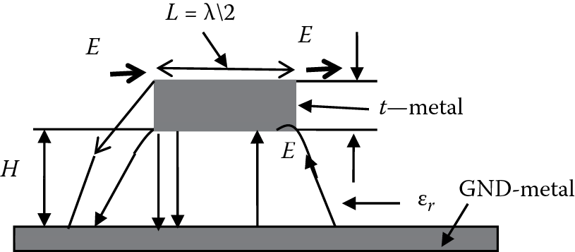
Microstrip antennas are printed on a dielectric substrate with low dielectric losses. A cross section of the microstrip antenna is shown in Figure 3.1. Microstrip antennas are thin patches etched on a dielectric substrate εr. The substrate thickness, H, is less than 0.1 λ.
Advantages of microstrip antennas:
- Low cost to fabricate
- Conformal structures are possible
- Easy to form a large uniform array with half-wavelength spacing
- Light weight and low volume
Disadvantages of microstrip antennas:
- Limited bandwidth (usually 1%–5%, but much more is possible with increased complexity)
- Low power handling
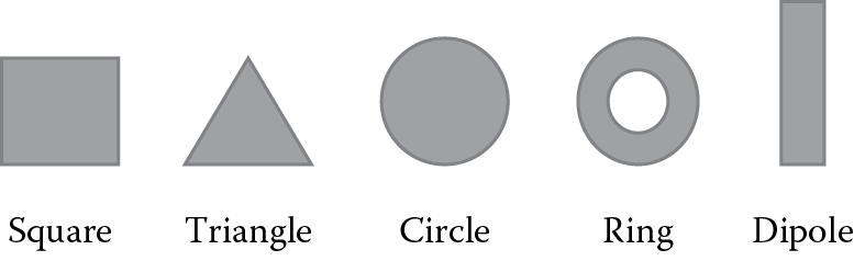
The electric field along the radiating edges is shown in Figure 3.2. The magnetic field is perpendicular to the E-field according to Maxwell’s equations. At the edge of the strip (X/L = 0 and X/L = 1) the H-field drops to zero; because there is no conductor to carry the radio frequency (RF) current, it is maximum in the center. The E-field intensity is at maximum magnitude (and opposite polarity) at the edges (X/L = 0 and X/L = 1) and zero at the center. The ratio of the E- to H-field is proportional to the impedance that we see when we feed the patch. Microstrip antennas may be fed by a microstrip line or by a coaxial line or probe feed. By adjusting the location of the feed point between the center and the edge, we can get any impedance, including 50 Ω. Microstrip antenna shape may be square, rectangular, triangle, circle, or any arbitrary shape as shown in Figure 3.3.

The dielectric constant that controls the resonance of the antenna is the effective dielectric constant of the microstrip line. The antenna dimension W is given by Equation 3.1.
(3.1)
The antenna bandwidth is given in Equation 3.2.
(3.2)
The gain of microstrip antenna is between 0 dBi and 7 dBi. The microstrip antenna gain is a function of the antenna dimensions and configuration. We may increase printed antenna gain by using a microstrip antenna array configuration. In a microstrip antenna array the benefit of a compact low-cost feed network is attained by integrating the RF feed network with the radiating elements on the same substrate. Microstrip antenna feed networks are presented in Figure 3.4. Figure 3.4 shows a parallel feed network. Figure 3.4 shows a parallel series feed network.

Configuration of microstrip antenna array. (a) Parallel feed network. (b) Parallel series feed network.
3.1.2 Transmission Line Model of Microstrip Antennas
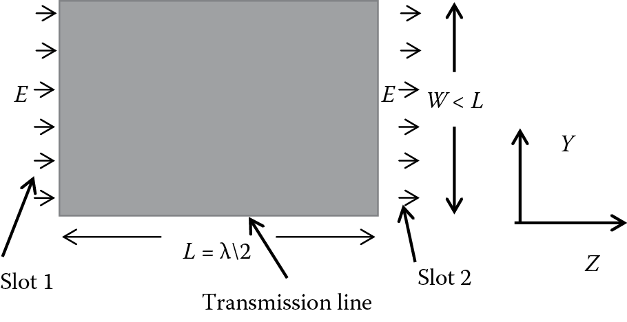
In the transmission line model (TLM) of patch microstrip antennas the antenna is represented as two slots connected by a transmission line (Figure 3.5). TLM is not an accurate model. However, it gives a good physical understanding of patch microstrip antennas. The electric fields along and underneath the patch depend on the z coordinate.
(3.3)
At z = 0 and z = Leff the electric field is maximum. At the electric field equals zero.
For the electric field distribution along the x-axis is assumed to be uniform. The slot admittance may be written as given in Equations 3.4 and 3.5.
(3.4)
(3.5)
B represents the capacitive nature of the slot. G = 1/R, where R represents the radiation losses. When the antenna is resonant the susceptances of both slots cancel out at the feed point for any position of the feed point along the patch. However, the patch admittance depends on the feed point position along the z-axis. At the feed point the slot admittance is transformed by the equivalent length of the transmission line. The width W of the microstrip antenna controls the input impedance. Larger widths can increase the bandwidth. For a square patch antenna fed by a microstrip line, the input impedance is around 300 Ω. By increasing the width, the impedance can be reduced.
(3.6)
3.1.3 Higher-Order Transmission Modes in Microstrip Antennas
To prevent higher-order transmission modes we should limit the thickness of the microstrip substrate to 10% of a wavelength. The cutoff frequency of the higher-order mode is given in Equation 3.7.
(3.7)
3.1.4 Effective Dielectric Constant
A part of the fields in the microstrip antenna structure exists in air and the other part of the fields exists in the dielectric substrate. The effective dielectric constant is somewhat less than the substrate’s dielectric constant. The effective dielectric constant of the microstrip line may be calculated by Equations 3.8 and 3.9 as a function of W/H.
For
(3.8)
For
(3.9)
This calculation ignores strip thickness and frequency dispersion, but their effects are negligible.
3.1.5 Losses in Microstrip Antennas
Losses in microstrip line are due to conductor loss, radiation loss, and dielectric loss.
3.1.5.1 Conductor Loss
Conductor loss may be calculated by using Equation 3.10.
(3.10)
Conductor losses may also be calculated by defining an equivalent loss tangent δc, given by δc = δs/h, where . Where σ is the strip conductivity, h is the substrate height and μ is the free space permeability.
3.1.5.2 Dielectric Loss
Dielectric loss may be calculated by using Equation 3.11.
(3.11)
3.1.6 Patch Radiation Pattern
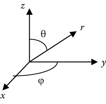
The patch width, W, controls the antenna radiation pattern. The coordinate system is shown in Figure 3.6. The normalized radiation pattern is approximately given by
(3.12)
(3.13)
The magnitude of the fields is given by
(3.14)
3.2 Two-Layer Stacked Microstrip Antennas
Two-layer microstrip antennas was presented first in Refs. [1,5–8]. The major disadvantage of single-layer microstrip antennas is narrow bandwidth. By designing a double-layer microstrip antenna we can get a wider bandwidth.
In the first layer the antenna feed network and a resonator are printed. In the second layer the radiating element is printed. The electromagnetic field is coupled from the resonator to the radiating element. The resonator and the radiating element shape may be a square, rectangle, triangle, circle, or any arbitrary shape. The distance between the layers is optimized to obtain maximum bandwidth with the best antenna efficiency. The spacing between the layers may be air or a foam with low dielectric losses.
A circular polarization double-layer antenna was designed at 2.2 GHz. The resonator and the feed network were printed on a substrate with a relative dielectric constant of 2.5 with thickness of 1.6 mm. The resonator is a square microstrip resonator with dimensions W = L = 45 mm. The radiating element was printed on a substrate with a relative dielectric constant of 2.2 with thickness of 1.6 mm. The radiating element is a square patch with dimensions W = L = 48 mm. The patch was designed as a circular polarized antenna by connecting a 3 dB 90° branch coupler to antenna feed lines, as shown in Figure 3.7. The antenna bandwidth is 10% for voltage standing wave ratio (VSWR) better than 2:1. The measured antenna beam width is around 72°. The measured antenna gain is 7.5 dBi. Measured results of stacked microstrip antennas are listed in Table 3.1.
Measured Results of Stacked Microstrip Antennas
|
Antenna |
F (GHz) |
Bandwidth (%) |
Beam Width (°) |
Gain (dBi) |
Side Lobe (dB) |
Polarization |
|
Square |
2.2 |
10 |
72 |
7.5 |
–22 |
Circular |
|
Circular |
2.2 |
15 |
72 |
7.9 |
–22 |
Linear |
|
Annular disc |
2.2 |
11.5 |
78 |
6.6 |
–14 |
Linear |
|
Rectangular |
2.0 |
9 |
72 |
7.4 |
–25 |
Linear |
|
Circular |
2.4 |
9 |
72 |
7 |
–22 |
Linear |
|
Circular |
2.4 |
10 |
72 |
7.5 |
–22 |
Circular |
|
Circular |
10 |
15 |
72 |
7.5 |
–25 |
Circular |

Results in Table 3.1 indicate that bandwidth of two-layer microstrip antennas may be around 9%–15% for VSWR better than 2:1. In Figure 3.7 a stacked microstrip antenna is shown. The antenna feed network is printed on a 1.6 mm thick FR4 dielectric substrate with dielectric constant of 4. The radiator is printed on a 1.6 mm thick RT/Duroid® 5880 dielectric substrate with dielectric constant of 2.2. The antenna electrical parameters were calculated and optimized by using ADS software. The dimensions of the microstrip stacked patch antenna shown in Figure 3.8 are 33 × 20 × 3.2 mm. The computed S11 parameters are presented in Figure 3.9. The radiation pattern of the microstrip stacked patch is shown in Figure 3.10. The antenna bandwidth is around 5% for VSWR better than 2.5:1. The antenna bandwidth is improved to 10% for VSWR better than 2.0:1 by adding 8 mm air spacing between the layers. The antenna beam width is around 72°. The antenna gain is around 7 dBi.

3.3 Stacked Monopulse Ku Band Patch Antenna
A monopulse double layer antenna was designed at 15 GHz. The monopulse double-layer antenna consists of four circular patch antennas as shown in Figure 3.11. The resonator and the feed network were printed on a 0.8 mm thick substrate with relative dielectric constant of 2.5. The resonator is a circular microstrip resonator with diameter a = 4.2 mm. The radiating element was printed on a 0.8 mm thick substrate with relative dielectric constant of 2.2. The radiating element is a circular microstrip patch with diameter a = 4.5 mm. The four circular patch antennas are connected to three 3 dB 180° rat-race couplers via the antenna feed lines, as shown in Figure 3.11. The comparator consists of three stripline 3 dB 180° rat-race couplers printed on a 0.8 mm thick substrate with relative dielectric constant of 2.2. The comparator has four output ports: a sum port Σ, difference port Δ, elevation difference port ∆E1, and azimuth difference port ∆Az as shown in Figure 3.11. The antenna bandwidth is 10% for VSWR better than 2:1. The antenna beam width is around 36°. The measured antenna gain is around 10 dBi. The comparator losses are around 0.7 dB.

3.3.1 Rat-Race Coupler
A rat-race coupler is shown in Figure 3.12. The rat-race circumference is 1.5 wavelengths. The distance from A to Δ port is 3λ4. The distance from A to Σ port is λ4. For an equal-split rat-race coupler, the impedance of the entire ring is fixed at 1.41 × Z0, or 70.7 Ω for Z0 = 50 Ω. For an input signal V, the outputs at ports 2 and 4 are equal in magnitude, but 180° out of phase.

3.4 Loop Antennas
Loop antennas are used as receive antennas in communication and medical systems. Loop antennas may be printed on a dielectric substrate or manufactured as a wired antenna. In this section several loop antennas are presented.
3.4.1 Small Loop Antenna
A small loop antenna is shown in Figure 3.13. The shape of the loop antenna may be circular or rectangular. These antennas have low radiation resistance and high reactance. It is difficult to match the antenna to a transmitter. Loop antennas are most often used as receive antennas, where impedance mismatch loss can be accepted. Small loop antennas are used as field strength probes, in pagers, and in wireless measurements.
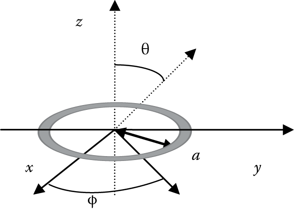
The loop lies in the x–y plane. The radius a of the small loop antenna is smaller than a wavelength (a << λ). A loop antenna electric field is given in Equation 3.17. A loop antenna magnetic field is given in Equations 3.15 and 3.16.
(3.15)
(3.16)
The variation of the radiation pattern with direction is sin θ, the same as for a dipole antenna. The fields of a small loop have the E and H fields switched relative to that of a short dipole. The E field is horizontally polarized in the x–y plane.
The small loop is often referred to as the dual of the dipole antenna, because if a small dipole had magnetic current flowing (as opposed to electric current as in a regular dipole), the fields would resemble that of a small loop. The short dipole has a capacitive impedance (the imaginary part of the impedance is negative). The impedance of a small loop is inductive (positive imaginary part). The radiation resistance (and ohmic loss resistance) can be increased by adding more turns to the loop. If there are N turns of a small loop antenna, each with a surface area S, the radiation resistance for small loops can be approximated as given in Equation 3.17.
(3.17)
For a small loop, the reactive component of the impedance can be determined by finding the inductance of the loop. For a circular loop with radius a and wire radius r, the reactive component of the impedance is given by Equation 3.18.
(3.18)
Loop antennas behave better in the vicinity of the human body than dipole antennas. The reason is that the electric near fields in dipole antennas are very strong. For r << 1, the dominant component of the field varies as 1/r3. These fields are the dipole near fields. In this case the waves are standing waves and the energy oscillates in the antenna near zone and is not radiated to the open space. The real part of the Poynting vector is equal to zero. Near the body the electric fields decay rapidly. However, the magnetic fields are not affected near the body. The magnetic fields are strong in the near field of the loop antenna. These magnetic fields give rise to the loop antenna radiation. The loop antenna radiation near the human body is stronger than the dipole radiation near the human body. Several loop antennas are used as “wearable antennas.”
3.4.2 Printed Loop Antenna
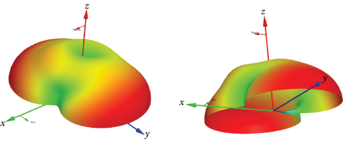
The diameter of a printed loop antenna is around a half wavelength. A loop antenna is dual to a half-wavelength dipole. Several loop antennas were designed for medical systems at frequency ranges between 400 MHz and 500 MHz. In Figure 3.14 a printed loop antenna is presented. The antenna was printed on FR4 with 0.5 mm thickness. The loop diameter is 45 mm. The loop antenna VSWR is around 4:1. The printed loop antenna radiation pattern at 435 MHz is shown Figure 3.15. The loop antenna gain is around 1.8 dBi. An antenna with a tuning capacitor is shown in Figure 3.16. The loop antenna VSWR without the tuning capacitor was 4:1. This loop antenna may be tuned by adding a capacitor or varactor as shown in Figure 3.17. Matching stubs are employed to tune the antenna to the resonant frequency. Tuning the antenna allows us to work in a wider bandwidth as shown in Figure 3.18. Loop antennas are used as receive antennas in medical systems. The loop antenna radiation pattern on the human body is shown Figure 3.19. The computed 3D radiation pattern and the coordinate used in this chapter are shown in Figure 3.19.


3.4.3 Radio Frequency Identification Loop Antennas
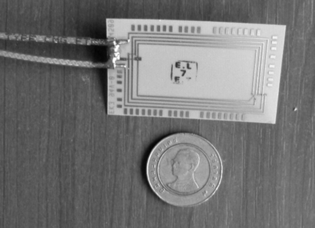
Radio frequency identification (RFID) loop antennas are widely used. Several RFID loop antennas are presented in Ref. [10]. RFID loop antennas have low efficiency and narrow bandwidth. As an example, the measured impedance of a square four-turn loop at 13.5 MHz is 0.47 + j107.5 Ω. A matching network is used to match the antenna to 50 Ω. The matching network consists of a 56 pF shunt capacitor, 1 kΩ shunt resistor, and another 56 pF capacitor. This matching network has narrow bandwidth. The antenna is printed on a FR4 substrate. The antenna dimensions are 32 × 52.4 × 0.25 mm. The antenna layout is shown in Figure 3.20. A photo of the RFID antenna is shown in Figure 3.21. S11 results of the printed loop antenna are shown in Figure 3.22. The antenna S11 parameter is better than –9.5 dB without an external matching network. The computed radiation pattern is shown in Figure 3.23. The RFID antenna beam width is around 160°.


3.4.4 New Loop Antenna with Ground Plane
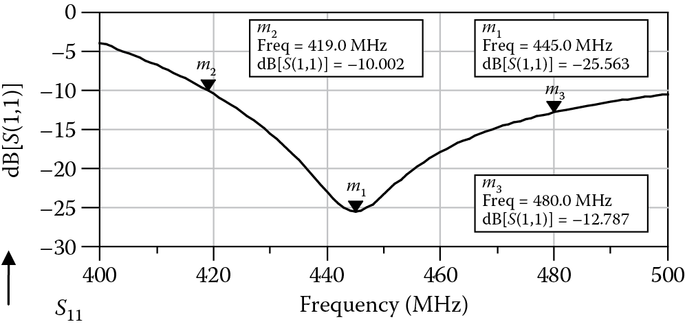
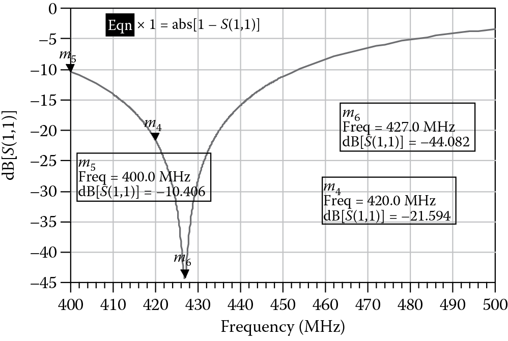
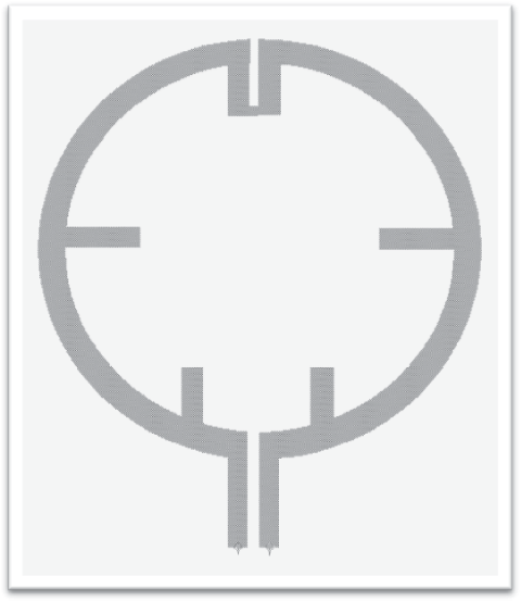
A new loop antenna with ground plane has been designed on Kapton substrates with a relative dielectric constant of 3.5 and thickness of 0.25 mm. The antenna is shown in Figure 3.24. Matching stubs are employed to tune the antenna to the resonant frequency. The loop antenna with ground plane diameter is 45 mm. The antenna was designed by employing ADS software. The antenna center frequency is 427 MHz. The antenna bandwidth for VSWR better than 2:1 is around 12%, as shown in Figure 3.25. The printed loop antenna radiation pattern at 435 MHz is shown in Figure 3.26. The loop antenna gain is around 1.8 dBi. The loop antenna with ground plane beam width is around 100°.


A printed loop antenna with ground plane with shorter tuning stubs is shown in Figure 3.٢٧. The loop antenna with ground with shorter tuning stubs plane diameter is 45 mm. The antenna center frequency is 438 MHz. The antenna bandwidth for VSWR better than 2:1 is around 12%, as shown in Figure 3.28. A printed loop antenna with shorter tuning stubs radiation pattern at 435 MHz is shown Figure 3.29. The loop antenna gain is around 1.8 dBi. The loop antenna with ground plane beam width is around 100°. A printed loop antenna with a shorter tuning stub 3D radiation pattern at 430 MHz is shown Figure 3.30.


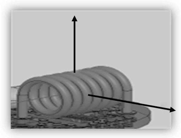
3.5 Wired Loop Antenna
A wire seven-turn loop antenna is shown in Figure 3.31. The antenna length l = 4.5 mm. The loop diameter is 3.5 mm. Equation 3.19 is an approximation to calculate the inductance value for an air coil loop antenna with N turns, diameter r, and length l.

(3.19)
An approximation to calculate the inductance value for an air coil loop antenna with N turns, diameter r, and length l is given in Equation 3.20.
(3.20)
For length l = 4.5 mm, wire diameter 0.6 mm, loop diameter 3.5 mm, and N = 7 the inductance is around L = 52 nH. The quality factor of this seven-turn wire loop is around 100. For length l = 1.7 mm, wire diameter 0.6 mm, loop diameter 6.5 mm, and N = 2 the inductance is around L = 45 nH. For length l = 2 mm, wire diameter 0.6 mm, loop diameter 7.62 mm, and N = 2 the inductance is around L = 42.1 nH. For length l = 0.5 mm, wire diameter 0.6 mm, loop diameter 7 mm, and N = 2 the inductance is around L = 87 nH. For length l = 2.5 mm, wire diameter 0.6, loop diameter 5 mm, and N = 2 the inductance is around L = 20.7 nH.
The wire loop antenna has very low radiation efficiency. The amount of power radiated is a small fraction of the input power. The antenna efficiency is around 0.01%, –41 dB. The ratio between the antenna’s dimension and wavelength is around 1:100. Small antennas are characterized by radiation resistance Rr. The radiated power is given by I2Rr, where I is the current through the coil. Remember that the current through the coil is Q times the current through the antenna. For example, for current of 2 mA and Q of 20, if Rr = 10–3 Ω, the radiated power is around –32 dBm.
Figure 3.32 presents a wire loop antenna with 2.5 turns on a PCB board. Figure 3.33 presents a wire loop antenna with seven turns on a PCB board.

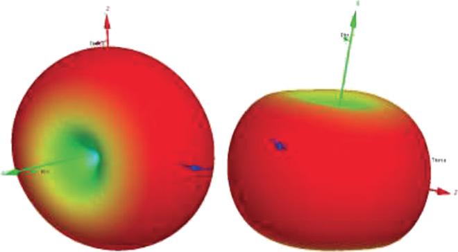
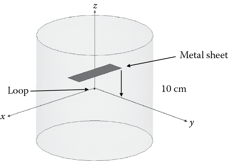
3.6 Radiation Pattern of a Loop Antenna Near a Metal Sheet
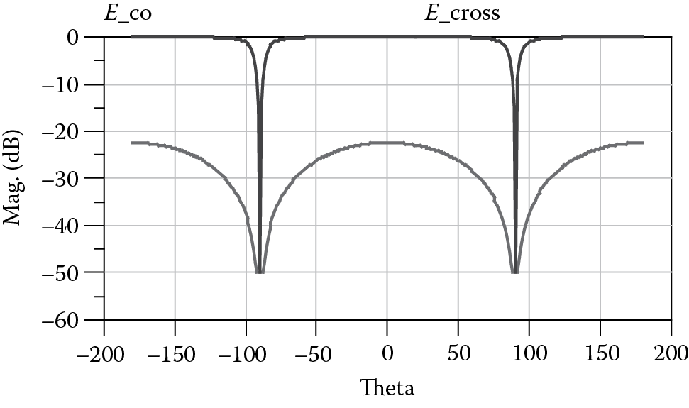
An E- and H-plane 3D radiation pattern of a wire loop antenna in free space is shown in Figure 3.34. An E- and H-plane 3D radiation pattern of a wire loop antenna near a metal sheet as shown in Figure 3.35 was computed by employing HFSS software. Figure 3.36 presents the E- and H-plane radiation pattern of loop antenna for distance of 30 cm from a metal sheet. We can see that a metal sheet in the vicinity of the antenna split the main beam and creates holes of around 20 dB in the radiation pattern. Figure 3.37 presents the E- and H-plane radiation pattern of loop antenna located 10 cm from a metal sheet as presented in Figure 3.38. We can see that a metal sheet in the vicinity of the antenna split the main beam and creates holes up to 15 dB in the radiation pattern.


E- and H-plane radiation pattern of a loop antenna for a distance of 30 cm from a metal sheet.
E- and H-plane radiation pattern of a loop antenna for distance of 10 cm from a metal sheet.
3.7 Planar inverted-F antenna
The planar inverted-F antenna (PIFA) possesses attractive features such as low profile, small size, and low fabrication costs [16–18]. The PIFA antenna bandwidth is higher than the bandwidth of the conventional patch antenna, because the PIFA antenna thickness is higher than the thickness of patch antennas. The conventional PIFA antenna is a grounded quarter-wavelength patch antenna. The antenna consists of ground-plane a top plate radiating element printed on a dielectric substrate, feed wire, and a shorting plate or short circuited via holes from the radiating element to the ground-plane as shown in Figure 3.39.

The patch is shorted at the end. The fringing fields, which are responsible for radiation, are shorted on the far end, so only the fields nearest the transmission line radiate. Consequently, the gain is reduced, but the patch antenna maintains the same basic properties as a half-wavelength patch. However, the antenna length is reduced by 50%. The feed location may be placed between the open and the shorted end. The feed location controls the antenna input impedance.
3.7.1 Grounded Quarter-Wavelength Patch Antenna
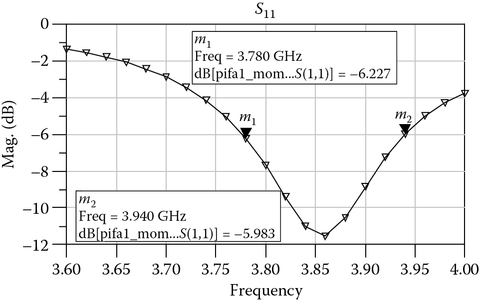
A grounded quarter-wavelength patch antenna was designed on a 1.6 mm thick FR4 substrate with relative dielectric constant of 4.5 at 3.85 GHz. The antenna is shown in Figure 3.40. The antenna was designed by using ADS software. The antenna dimensions are 34 × 17 × 1.6 mm. S11 results of the antenna are shown in Figure 3.41. The antenna bandwidth is around 6% for VSWR better than 3:1 without a matching network. The radiation pattern is shown in Figure 3.42. The antenna beam width is around 76°. The grounded quarter-wavelength patch antenna gain is around 6.7 dBi. The antenna efficiency is around 92%.


3.7.2 A New Double-Layer PIFA Antenna
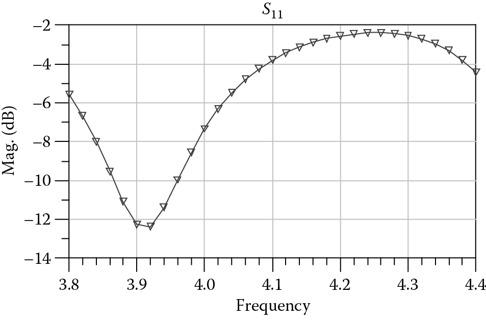
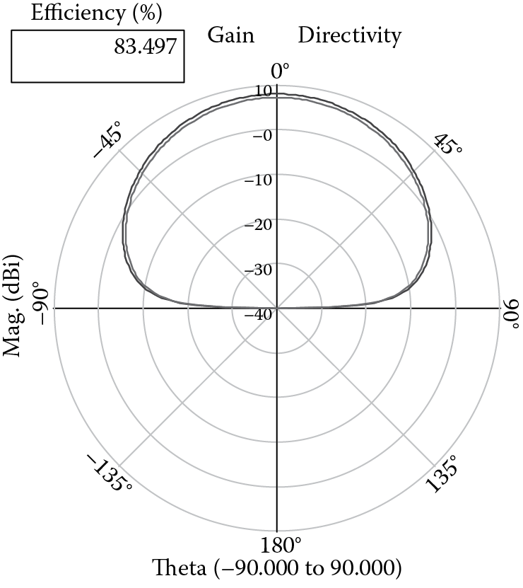
A new double-layer PIFA antenna was designed. The first layer is a grounded quarter-wavelength patch antenna printed on a 1.6 mm thick FR4 substrate with relative dielectric constant of 4.5. The second layer is a rectangular patch antenna printed on a 1.6 mm thick Duroid substrate with relative dielectric constant of 2.2. The antenna is shown in Figure 3.43. The antenna was designed by employing ADS software. The antenna dimensions are 34 × 17 × 3.2 mm. S11 results of the antenna are shown in Figure 3.44. The antenna is a dual-band antenna. The first resonant frequency is 3.48 GHz. The second resonant frequency is 4.02 GHz. The radiation pattern is shown in Figure 3.45. The antenna beam width is around 74°. The antenna gain is around 7.4 dBi. The antenna efficiency is around 83.4%.


References
1. James, J. R., Hall, P. S., and Wood, C. Microstrip Antenna Theory and Design. The Institution of Engineering and Technology, London, 1981.
2. Sabban, A., and Gupta, K. C. Characterization of Radiation Loss from Microstrip Discontinuities Using a Multiport Network Modeling Approach. IEEE Transactions on Microwave Theory and Techniques, 39(4):705–712, 1991.
3. Sabban, A. Multiport Network Model for Evaluating Radiation Loss and Coupling Among Discontinuities in Microstrip Circuits. PhD Thesis, University of Colorado at Boulder, January 1991.
4. Kathei, P. B., and Alexopoulos, N. G. Frequency-Dependent Characteristic of Microstrip, Discontinuities in Millimeter-Wave Integrated Circuits. IEEE Transactions on Microwave Theory and Techniques, MTT-33, 1029–1035, 1985.
5. Sabban, A. A New Wideband Stacked Microstrip Antenna. In IEEE Antenna and Propagation Symposium, Houston, TX, June 1983.
6. Sabban, A. Wideband Microstrip Antenna Arrays. In IEEE Antenna and Propagation Symposium MELCOM, Tel Aviv, Israel, June 1981.
7. Sabban, A. Microstrip Antennas. In IEEE Symposium, Tel Aviv, Israel, October 1979.
8. Sabban, A., and Navon, E. A mm-Waves Microstrip Antenna Array. In IEEE Symposium, Tel Aviv, Israel, March 1983.
9. de Lange, G. et al. A 3*3 mm-Wave Micro Machined Imaging Array with Sis Mixers. Applied Physics Letters, 75(6):868–870, 1999.
10. Rahman, A. et al. Micromachined Room Temperature Microbolometers for mm-Wave Detection. Applied Physics Letters, 68 (14):2020–2022, 1996.
11. Milkov, M. M. Millimeter-Wave Imaging System Based on Antenna-Coupled Bolometer. MSc. Thesis, UCLA, 2000.
12. Jack, M. D. et al. US Patent 6329655, 2001.
13. Sinclair, G. N. et al. Passive Millimeter Wave Imaging in Security Scanning. Proceedings of SPIE, 4032:40–45, 2000.
14. Kompa, G., and Mehran, R. Planar Waveguide Model for Computing Microstrip Components. Electronic Letters, 11(9):459–460, 1975.
15. Luukanen, A. et al. US Patent 6242740, 2001.
16. Wang, F., Du, Z., Wang, Q., and Gong, K. Enhanced-Bandwidth PIFA with T-shaped Ground Plane. Electronic Letters, 40(23):1504–1505, 2004.
17. Kim, B., Hoon, J., and Choi, H. Small Wideband PIFA for Mobile Phones at 1800 MHz. In Vehicular Technology Conference, Milan, Italy, Vol. 1, pp. 27–29, May 2004.
18. Kim, B., Park, J., and Choi, H. Tapered Type PIFA Design for Mobile Phones at 1800 MHz. In Vehicular Technology Conference, Stockholm, Sweden, Vol. 2, pp. 1012–1014, April 2005.