
13
PIC Family Microcontrollers
Chapter Outline
- Study basic features in PIC architecture
- Study PIC family MCU devices for the systems
- Learn interrupt sources, IC ports, timers and instruction set of PIC
- Learn MPLAB tool for integrated development environment (IDE)
An MCU has the following resources: memory, ports, serial IO (input and output) devices, timers and interrupt sources. There may be additional resources also. We learnt earlier in detail the resources in the 8-bit —8051/8031 family MCUs.
This chapter describes PIC microcontroller. The PIC stands for Programmable Microchip Intelligent Computer, also for Programmable Interface Controller. The PIC family microcontrollers (MCUs) are from Microchip technology (http://www.microchip.com).
13.1 PIC FAMILY
A PIC microcontroller characteristics are as follows: power-on reset, brown out reset, simplified instruction set, high speed execution, up to 25 mA output pin drive, programming by serial synchronous pins, watchdog timer, parallel slave port (PSP), SPI, USART, analog input ports, in-circuit debugger, and free integrated development environment (IDE), assembler and simulator.
C versions have EPROM (Erasable and programmable Read Only memory) and F versions are having flash memory.
13.1.1 MCU families
PIC MCUs are as follows:
- 12Cxxx family is for the 12/14 bit internal operations, 33/35 instructions and 0. 4μs instruction cycle time (minimum time for instruction execution).
- PIC12F675 is high-performance microcontroller with flash memory (F stands for the flash memory version). 12F675 has 1k of code space (program memory), 64 bytes of RAM, 128 bytes of EEPROM and runs up to 20 MHz clock speed.
- 16C5xx family is for 12 bit internal operations, 33 instructions and 0.2 μs (200 ns) instruction cycle time. 16C/Fxx family is for 14 bit internal operations, 35 instructions and 0.2 μs time instruction cycle time.
Example 13.2:
- PIC 16F877A is high-performance microcontroller with flash memory. It has 8 k × 14 code space, 368 bytes RAM and 256 bytes of EEPROM. It has single-cycle (0.2 μs) instructions for all except branch instruction. Branch takes two cycles. It has 20 MHz clock.
- 17C5xx family is for16 bit internal operations, 58 instructions and 0.12 μs time for instruction cycle time. 17C5xx is for 16 bit enhanced internal operations, 77 instructions and 0.1 μs time (minimum instruction execution time). 18Fxxx MCUs are for the new and advanced features.
Example 13.3:
- PIC 18F452 is high-performance microcontroller with flash memory. It has 16 kB of code space, 1536 bytes of RAM and 256 bytes of EEPROM. It has thus twice the program memory space and four times more RAM. It has two times the speed. It can run up to 40 MHz clock speed. [X-Tal of 10 MHz and a 4.7 MOhm resistance between OSC1 and OSC2 pins are used and then PLL (phased locked loop) option is enabled when programming the chip. The internal clock thus multiplies four times.] PIC 18F4550 has USB interface.
- PIC32 family MCU is the 32-bit microcontroller. It gives highest DMIPS per MHz clock operation. The MCU has an efficient internal bus architecture. The MCUs of the family have advanced feature of instruction caching and provides the DMA controller channels. Flash memory in MCUs can be 32 kB to 512 kB and on-chip RAM from 8 kB to 128 kB. An MCU of the family integrates with CAN, USB and Ethernet buses.
Example 13.4:
PIC32 clock (internal) operations are at 80 MHz. It has the 256 B cache and flash pre-fetch module. Performance is 1.56 DMIPS per MHz. It has single cycle multiply and division unit. It has atomic bit manipulation unit. [No interrupt till bit-manipulation completes.] It has fast context switching. [CPU data and status registers save automatically on call or interrupt and restore automatically.] It has 8-channel DMA controller. It has nested vector interrupt controller. [When an ISR is running, it can be interrupted by a higher priority interrupt event.] It has 10-bit ADC with 1 M samples per second. It has 16-bit parallel port. It operates at 2.3–3.6V. It can function up to 5 V IOs.
13.2 HARDWARE OF PIC 16F877
The Web site of Microchip http://www.microchip.com/wwwproducts/Devices.aspx?dDocName=en010241 gives the details about PIC 16F877. Datasheet for PIC 16F877 is at the site http://www.microchip.com/downloads/en/DeviceDoc/30292c.pdf.
13.2.1 Overview of the internal hardware in PIC MCU
Figure 13.1 shows a simple overview of the internal hardware. It shows the registers. It shows the buses for the ALU operations in a PIC. Following are the CPU features:
- MCU supports 8-bit operations. Internal data bus is of 8-bits.
- PIC family ALU operations are between the Working (W) register (accumulator) and register (or internal RAM) of a register-file. ALU operations can also be between the W and 8-bits operand from instruction register (IR). The operations also use three flags Z, C and DC/borrow. [Zero flag, Carry flag and digit (nibble) carry flag].
- Three bits Z, C and DC/borrow are the flags generated in the operations. [For borrow, the polarity reverses. On the carry during addition, the DC sets. On the borrow during subtraction, the DC resets.]
- The destination of result from ALU operations can be either W or register (f) in file. The flags save at status register (STATUS).PIC CPU is a one-address machine (one operand specified in the instruction for ALU); two operands are used in an arithmetic or logic operations, one is source operand from one register file/RAM (or operand from instruction) and another is from W-register. It gives advantage that ALU directly operates on a register or memory.

Figure 13.1 Internal Hardware for ALU Operations in a PIC Family MCU
Table 13.1 gives meanings of the symbols and signals. It gives the uses of structural units.
TABLE 13.1 The Meaning and Uses of the Signals and Structural Units Shown in Block Diagram
| Symbol | Full Form | Use |
|---|---|---|
ALU |
Arithmetic Logic Unit |
Unit to perform register arithmetic or logic unit (RALU) operation on the operands in W-register and Temp. These registers have operands from the registers/memory at an instance as per the instruction to be executed. The ALU gives the result(s) in source 1 (W) or source2 (Temp) |
PC |
Program Counter |
13-bit register to hold the program-memory address of the instruction being currently fetched; Increments continuously to point to the next instruction, unless there is change in path of program flow |
MUX |
data Multiplexer Data Unit |
Multiplexer for data from data bus and immediate operand, |
IR |
Instruction Register |
14-bit Instruction Register to hold the current instruction opcode and operand bits |
ID |
Instruction Decoder |
Instruction-decoder register to decode the IR opcode bits and activate the appropriate signals for controller and sequential circuits |
STATUS |
8-bit status |
STATUS has the flag bits C, DC, Z, PD, TO, and select bits RP0, RP1 and IRP. |
AddrMux |
Address Multiplexer |
Multiplexer for address for sending 9-bits for selecting a register from register file/RAM or memory address at RAM |
8-level stack |
8-word Stack |
13-bit stack for the PC and is eight level deep. It functions as circular buffer (if 9th level value of PC is pushed then it will replace the first value of PC in the stack. |
13.2.2 Architecture of PIC Microcontroller
Figure 13.2 shows architecture of a PIC-family MCU 16F877.
MEMORY HARVARD ARCHITECTURE
- CPU of PIC processes the instructions using Harvard architecture for memory. Harvard architecture means separate address spaces for the program and data.
The PIC memory architecture has separate address spaces for the (i) data memory for special function registers (SFR), registers and internal RAM, (ii) EEPROM data memory and (iii) program memory, interrupt vectors, constant data and text (flash memory). Separate internal buses are there for the address of 13-bit A0-A12 for the program address in 16F877, program code-bus of 14-bit and data D0-D7 of 8-bit. Flash memory retention period is more than 40 years.

PROGRAM COUNTER AND INTERNAL PROGRAM MEMORY BUS
- Program memory is of 8 k × 14. Program address-fetch bus is of 13-bit. There are thus 8192 program instruction addresses. Program counter is thus of 13-bit word pointing to one of the 8 k (8192) addresses in program memory (flash).
- Instruction length is 14-bit. Program-code bus is of 14-bit.
- Flash saves 14-bits at each address. 8192 addresses are present in flash in PIC 16F877.
- Program Counter starts from a value, which is pre-programmed at the reset vector address. Reset vector address is 0x0000 in program memory. Reset vector means the memory location from where the processor will find the address of the program codes to be executed after the reset or on-power-up.
5. Data bus interconnects the registers, RAM, internal peripherals and ports. Data bus has 8-bit width.
6. W-register and STATUS register, both are of 8-bits. These are present at the internal data bus.
INSTRUCTION CYCLE TIME
7. Instruction cycle time is 0.2 μs (200 ns) and thus executes 5 MIPS (million instruction per second).
REGISTER FILE/RAM
8. Register file/RAM is of 368 B in PIC 16F877. 9-bits are required to access the RAM. Therefore, the register file/RAM divides in four banks. Each bank has 128 addresses. Each bank register/ RAM therefore accesses by 7-bit address. Bank is decided for the access by the RP1:RP0 bits. A 7-bit address is used when using direct address for a register/RAM. This address plus the bank base address generates 9-bit address of a register/internal RAM.
9. Four banks of Registers/RAM are as follows:. The register/RAM in bank0 is at address between 0x000 and 0x07F. The register/RAM in bank1 is at address between 0x080 and 0x0FF. The register/RAM in bank2 is at address between 0x100 and 0x17F. The register/RAM in bank3 is at address between 0x180 and 0x1FF.
10. Four banks form two pairs of banks of Registers/RAM. The register/RAM in lower bank pair bank0-bank1 is at address between 0x000 and 0x0FF. The register/RAM in upper bank pair bank2-bank3 is at address between 0x100 and 0x1FF. Bank-pair 0 address is 0x000 and 1 address is 0x100.
11. Each bank pair register/RAM accesses by 8-bit address. Bank pair is as per IRP bit. 8-bit address is used when using indirect address for a register/RAM. This address plus the bank-pair base address generates 9-bit address of a register/internal RAM.
RAM/FILE REGISTER SELECT REGISTER (FSR)
12. There is a file select register (FSR) of 8-bits. It provides the 8-bit address of RAM/register in the register file. That address is in which bank-pair, this is as per IRP bit in the STATUS. The FSR is used for indirect addressing in the instruction.
STATUS REGISTER (STATUS)
13. The STATUS has 8-bits. Bit 0, 1, 2 are C, DC/borrow and Z.
14. Indirect address has 8-bits. These bits are taken from address at either lower pair or upper pair. Bit 7 IRP (indirect register-bank pair) bit in STATUS, when = 1, then upper bank-pair is used and when = 0 then lower bank pair is used.
15. Direct address has taken from 7-bits in the instruction. They are taken for either bank 0 or 1 or 2 or 3. Bit 6-5 RP1-RP0 (register-pair higher bank-register pair lower bank) bits in STATUS, when = 11, then higher bank 3. When = 10, then bank 2. When = 01, then bank 1. When = 00, then bank 0.
16. Bit 4 of STATUS is TO (time-out) bit. TO =0 means that watchdog timer (WDT) timeout has occurred, = 1 means still not occurred. TO = 1 after power-up also. TO is 1 after CLRWDT (clear watchdog timer) instruction also.
17. Bit 3 of STATUS is PD (power-down) bit. PD=0 means sleep status after SLEEP instruction. PD = 1 after power-up. PD is 1 after CLRWDT (clear watchdog timer) instruction also.
18. MUX takes 8-bit input from either (i) 8-bit instruction register during the instruction with immediate addressing or branch or call or (ii) data from register file/RAM or data-bus.
19. ADDRMUX takes 8-bit input indirect address bits or 7-bit direct address from IR during instruction immediate addressing or branch or call instruction. An instruction may use a 7-bit direct address for addressing a register/RAM. ADDRMUX then gives 9-bit output address for a register or RAM.
MEMORY AND PERIPHERALS IN ARCHITECTURE OF PIC16F877
The following are the memory, peripherals and circuits in PIC16F877:
- Program memory size is 14 kB (8 k × 14 bit instructions). Program memory type is flash.
- It has RAM of 368 bytes and data EEPROM of 256 bytes. Internal RAM of 368 byte is common to 256 B register file with registers divided in banks. There is also an additional 256-byte EEPROM.
- The synchronous serial port can be configured as 3-wire Serial Peripheral Interface (SPI™) option 1. The option 2 is 2-wire Inter-Integrated Circuit (I2C™) bus and a Universal Asynchronous Receiver Transmitter (USART). Two data communication peripherals are 1-A/E/USART (universal synchronous asynchronous receiver and transmitter) and 1-MSSP (SPI/I2C). [MSSP (master synchronous serial port) operate in master SPI mode or master/slave mode I2 C.]
- There are two 8-bit timers, TMR0 and TMR2 2 × 8-bit (Section 13.5).
- There is one 16-bit timer, TMR1 1 × 16-bit (Section 13.5).
- There is CCP1, 2. It has two capture/compare/PWM peripherals for input capture, out-compare and pulse width modulation functions.
- There is 8-input channel 10-bit ADC.
- MCU operates at 2.0 V to 5.5 V and has 40-pins.
- The clock (oscillator) and reset circuits are the internal circuits.
- A XTAL is attached at two pins OSC1 and OSC2. There is 20 MHz Oscillator. It connects the OSC1 and OSC2 pins. OSC circuit has four options (Table 13.2)
- Reset Circuit, which connects to
 pin. /Vpp = 0 for the reset.
 - pin is also used as Vpp (Programming voltage). The Vpp is also applied at this pin when programming the MCU. [Programming means writing the program codes to internal flash memory.]
- One external interrupt is provided. It occurs through PORTB RB0 pin.
- Harvard architecture: There is the internal flash starting from program code address 0x0000 (Program memory) accessed by 13-bits. There is the internal RAM/register file for the SFRs/GPRs(general purpose registers)/RAM) starting from 0x0000 and 0x000 (Data memory). It is accessed by 7-bit direct address or 8-bit indirect address.
- Ports: There are five Ports— 6-bit PORTA, 8-bit PORTB, 8-bit PORTC, 8-bit PORTD, and 3-bit PORTE. Each port has a data-direct register TRIS. A TRIS (transmit-receive input select) bit controls the direction of a port pin, whether it will be for input or for output. These are called TRISA, TRISB, TRISC, TRISD and TRISE for A, B, C, D and E ports, respectively.
- Parallel Slave Port: PSP is a handshake mode port in which Port D pins are used for PSP input/output and Port E pins are used for control signals
 ,
,  and
and  . PORTD can either function as general purpose port or PSP. PSP control and status bits are at TRISE b4, b5, b6 and b7 bits and the control signals are through PORTE when PORTD is programmed for the PSP (Section 13.4).
 - Register file/internal RAM: Between 0x000 and 0x1FF, there is register file/internal RAM. A register file is of 256 bytes in 4 banks (two bank-pairs). Each bank is of 128 byte and registers/RAM has the data at 7-bit addresses 0x00 to 0x7F. in a bank. Bank base address starts from address 0x08×bank number (0 or 1 or 2 or 3) [Lower addresses in a bank are for the SFRs. Higher addresses are for the GPRs.] (Section 13.3).
- 14 kB flash has the addresses of vectors, program, routines, ISRs and its constant data starting from 0x0000 and extending up to 0x1FFF (8192 addresses, accessible by 13-bits).
- A program word is of 14-bit length. Reset vector and interrupt vectors are between 0x0000 and 0x0004. Program memory divides into four pages. Page 0 program memory address starts from 0x0005, page 1 from 0x07FF, page 2 from 0x1000 and page 3 from 0x17FF aligns at the even and odd addresses that correspond to lower and upper bytes, respectively.
- There is an interrupt control circuit. INTCON is used for defining control bits for timer 0 overflow, port B input change and external pin INT interrupts. It also defines the global interrupt enable and peripherals interrupt (service) enable.
- There is a watchdog timer unit that can be set to reset the processor after watched-time for finishing a task is over.
- There are following circuits power-up timer, oscillator start-up timer, power-on reset, brown out reset, in-circuit debugger and low V programming. [Brown-out circuit means a circuit, which detects the voltage VDD falling below a threshold then it resets the MCU] Programming means writing the program codes to internal flash memory/EPROM.
Table 13.2 gives the supply subunits and devices that are present in PIC family MCU version 16F877. It also gives the use of meanings of the symbols used in Fig.13.2 for the INT, reset, OSC/XTAL pins.
TABLE 13.2 The Subunits in the Reset, OSC/XTAL and Supply Subunits and the Uses
| Symbol | Full Form | Use |
|---|---|---|
|
Master clear when 0 |
External reset pin for the chip reset. Also used as Vpp for applying programming voltage input |
CLKIN/OSC1/XTAL1 and CLKOUT/OSC2/ XTAL2 |
Pins to the crystal/oscillator |
Option 1: LP Low power crystal, Option 2: XT crystal (up to 4 MHz), Option 3: HS high speed crystal/ resonator (up to 16 MHz) and 20 MHz crystal Option 4: RC Resistor/capacitor |
VDD |
Voltage Supply Pin |
For 2 V to 5 V supply |
VSS (GND) |
Supply Ground |
Ground |
V-ref Analog GND |
Analog-in as well as V-ref |
Common pins for analog input and of −ve reference voltage |
V+ref |
V+ref Positive voltage |
Reference input to reference the maximum analog input after scalinga, upto which the input is measurable. [Kept at about 1 or 2 V.] |
a Scaling means signal conditioning of analog input so that its variations are within the V-ref and V+ref
13.2.3 Features of the CPU of PIC 16F877
The following are the features of the CPU:
Initial Conditions
On power up reset or other reset for example by RST instruction, the IOs, timer and other control SFRs, PC, flags in PSW acquire the same value as acquired on CPU power up, and all three flags Z, C and DC/borrow get reset. (ii) Send a pulse at reset pin to enable reset of other interfaced programmable peripherals. The datasheet can be used for the values of the SFRs on POR, BOR, ![]() /WDT reset and wake-up through WDT or interrupt.
/WDT reset and wake-up through WDT or interrupt.
POR, BOR, ![]() /WDT Reset
/WDT Reset
PCL becomes 00000000 defining PC lower 8-bits on POR, BOR and ![]() /WDT reset. PCLATH (PC address translation higher bits defining PC higher 5-bits) becomes 00000 on POR, BOR and
/WDT reset. PCLATH (PC address translation higher bits defining PC higher 5-bits) becomes 00000 on POR, BOR and ![]() / WDT reset. TRISA (6-bits), TRISB (8-bits), TRISC (8-bits), TRISD (8-bits) and TRISE(3-bits) become 1s. This means all port pins directions are input. OPTIO_REG and PR2 bits become 1s. Bits related to interrupts in PIE, PIE2, PIR1 and register become 0s.
/ WDT reset. TRISA (6-bits), TRISB (8-bits), TRISC (8-bits), TRISD (8-bits) and TRISE(3-bits) become 1s. This means all port pins directions are input. OPTIO_REG and PR2 bits become 1s. Bits related to interrupts in PIE, PIE2, PIR1 and register become 0s.
![]() /WDT Reset
/WDT Reset
PORTB, PORTC, PORTD, PORTE, timer holding registers, TMR0 and TMR1 and CCP1L, CCP1H, CCP2L and CCP2H remain unchanged.
Wake-up Through WDT or Interrupt
All PR2 bits in timer T2 become 1s. PCLATH (5-bits) do not change on the wake-up. Wake-up through WDT or interrupt changes only the PCL. PCL becomes PC + 1 on wake-up through WDT or interrupt. [When the wake-up is due to interrupt then of GIE (global interrupt enable bit) is set then PC acquires the value from address 0x0004 (interrupt vector address). Other register bits remain unchanged.
Selection of Oscillator
Four types of oscillators are available. An oscillator is selectable by FOSC1:FOSC0 (frequency oscillator selection bits). These are bit b1-b0 at 14-bit CONFIGURATION word. The word is at program memory address 0x2007. Bits 11,10, 01 and 00 select the RC, HS, XT and LP oscillator. RC is a resistor-capacitor based oscillator. Both R and C are externally connected. HS means high-speed Xtal oscillator/resonator of frequency 4 MHz or 8 MHz or 20 MHz. XT means Xtal oscillator of frequency 455 MHz or 2 MHz or 4 MHz. LP means low power Xtal oscillator of frequency 32 kHz or 0.2 MHz (200 kHz).
Reset Types
There are the following types of reset:
POR, BOR and ![]() Resets - and PWRT and OST Timers
Resets - and PWRT and OST Timers
- When VDD is detected > than 1.2–1.7 V, then power-on reset (POR) generates a pulse. The pulse can be used by connecting the pin to VDD (optionally through a resistor). Other peripherals might be connected to PIC. The pulse can then be used by other peripherals. It synchronizes their reset circuits.
- There is a power-up timer (PWRT). It provides 72 ms time-out on power-up and power-On reset. 72 ms is internally set by internal oscillator circuit with internal RC.
- There is Oscillator Start-up Timer (OST). It provides 1024 oscillation cycles delay after PWRT time-out. It lets the oscillator stabilize after the oscillations start.
- When VDD is detected < than VBOR about 4 V for a period > than 100 μs, then brown-out situation is detected and the brown-out reset (BOR) reset occurs. The process will restart when VDD becomes > than VBOR. If VDD becomes < than VBOR again during PWRT run, then BOR process will start again.
- There is a brown-up timer which gives a delay of 100 μs for the BOR reset on VDD is detected < than VBOR.
- There is PCON (power Control/Status Register). PCON bit b0 is BOR (brown-out reset status bit). User sets it as 1. The reset clears it and makes it 0, if BOR enabled. PCON bit b1 is POR (power-on reset status). User sets it as 1. The reset clears it and makes it 0. The user must set it as 1 on the occurrence of PRO reset.
![]() Reset
Reset
The reset also occurs when ![]() pin is made 0. The
pin is made 0. The ![]() reset takes place in two conditions: normal and SLEEP.
reset takes place in two conditions: normal and SLEEP.
WDT Reset
Bit WDTE bit b2 when 1 in configuration word, enables WDT else disables the WDT. Watchdog timer unit that can be set to reset the processor after watched-time for finishing a task is over. The WDT reset takes place in two conditions: normal and SLEEP. Time for the reset has two options: the WDT timer option or using timer TMR0 clock source. The PS2-PS1-PS0 (post scaling) bits can be used to divide the time set by one of two options.
Interrupt and Reset Vectors
Reset vector is at 0x0000 and interrupt vector at 0x0004 in program memory. Vector means a memory address from where the CPU will fetch the address of the new instruction for execution.
Configuration Word
There is 14-bit configuration word. It is at address 2007H.
- Bit FOSC1:FOSC0 b1–b0 selects one of the oscillator RC, HS, XT or LP.
- Bit WDTE bit b2 enables WDT when 1 else disables.
- Bit PWRTE bit b3 when 1, enables power up timer else disables.
- Bit BODEN bit b6 when 1, enables brown-out Reset else disables.
- Bit LVP bit b7 enables low voltage in-circuit serial programming. When 1, then RB3/PGM pin does PGM function, low voltage programming enabled else disables PGM low voltage programming.
- Bit CPD bit b8 when 1, enables data EE memory code protection else disables.
- Bit WRT bit b9 when 1, enables flash memory write else disables.
- Bit DEBUG bit b11 when 1, enables in-circuit debugger mode RB6 and RB7 else disables.
- Bit CP1:CP0 enables protection of code. The pair of bits in 16F877 when (i) 00 protects page 0, 1, 2 and 3, (ii) 01 protects page 1 higher 256 words protection, (iii) 10 protects page 3 higher 256 words protection and (iv) 11 makes code protection off.
It occurs when SLEEP instruction is executed. Oscillator can be turned off, therefore the program counter does not increment. Next instruction from PC+1 is prefetched for use on wake-up later. Sleep is called power-down mode. If WDT enabled before, then WDT is disabled.
Wake-up from SLEEP can be from one of three situations— RESET input at MCLR or external interrupt at INT or WDT wake-up if enabled. Wake-up from SLEEP can also be from PSP read or write, SSP start/stop bit detect interrupt, SSP (SPI or I2C) transmit/receive in slave mode interrupt, timer TMR1 interrupt, CCP special event trigger, CCP capture mode interrupt, USART RX or TX synchronous slave mode interrupt, AD conversion interrupt and EEPROM write complete interrupt.
CODE PROTECTION
CPD and CP1— CP bits of configuration word enables the code protection.
ID LOCATIONS
Program memory addresses 0x2000 to 0x2003 are called ID locations. These are used to write the check-sum or other identification numbers. Normal access does not allow read or write of ID. Access is permitted during programming or verifying the programmed memory.
In-Circuit Serial Programming
In-circuit programming takes place by appropriate serial inputs.
Low Voltage In-circuit Serial Programming
Bit LVP bit b7 of configuration word enables low voltage in-circuit serial programming. When 1, then RB3/PGM pin does PGM function, low voltage programming enabled else disables PGM low voltage programming.
In-circuit Debugging
Bit DEBUG bit b11 enables in-circuit debugger mode RB6 and RB7 when 1 else disable.
13.3 MEMORY AND MEMORY MAP IN MICROCHIP PIC FAMILY MCU SYSTEM
13.3.1 On-Chip SFRs/GPRs/Internal RAM, program memory and Data EEPROM
Table 13.3 gives the meanings of the symbols used in the data memory, program memory and data EEPROM that are present in PIC family MCU version 16F877. It also gives the use of each one.
TABLE 13.3 The SFRs/GPRs/Internal RAM, Program Memory and EEPROM in the Harvard Architecture
| Symbol | Full Form | Use |
|---|---|---|
SFRs |
Special Function Registers |
Control and status registers for the peripherals, input/ output and Interrupt. These are at direct as well as indirect addressable memory area for the register file. [Refer Figures 13.3 and 13.4. Tables 13.4, 13.5 and 13.6. SFR space is 32 B in Bank 0, 32 B in Bank1, 16 B in Bank2 and 16 B in Bank3.] |
GPRs/Internal RAM Register file |
For the read and write. [Refer Figure 13.4. The 96 B in Bank 0, 96 B in Bank 1, 80 B for Bank 2 and 80 B for Bank 3 memory are for the GPRs/ Internal Random Access memory; total 352 byte space. Highest 16B RAM addresses in each bank are common to all other banks.] |
|
Flash |
Flash Read Only Program Memory |
A write operation means erase and then write. Program memory can store instructions, constant data, calibration parameters, ASCII text etc.a |
Data EEPROM (on-chip memory) |
Electrically erasable and electrically programmable Read Only Program Data Memory |
A write operation means erase and then write. 256-byte EEPROM is present in 16F877. It stores run-time generated and updated values. The values are non-volatile (don’t change on power down). Read and write are through six SFRs. [EECON1 and EECON2, EEADRH-EEADR and EETATH-EEDATA.] |
a Fetch and access to invalid instruction results execution of NOP (no operation). Access to program memory allows for check-sum calculations. Read and write is through six SFRs [EECON1 and EECON2, EEADRH-EEADR and EETATH-EEDATA]. 14-bit data for write is placed at EEDATH-EEDATA. EEADRH-EEADR has 13-bit address in 16F877 (8 k × 14 flash version). The valid program memory addresses are between 0x0000 and 3FFF.
13.3.2 On-Chip Data Memory RAM
A 7-bit direct address is used for accessing 8-bits in a bank. Bank 0 is the address space between 0x00 and 0x7F. There are two Bank-pairs 0 or 1 for the four banks, 0, 1, 2 and 3. A register/RAM can be addressed by 8-bit indirect address also.
The PIC SFRs are directly addressable (by 7-bits) or as well as indirect addressable (by 8-bits) in an instruction. Figure 13.3 shows the addresses at banks/ bank pairs. A bank is identified by CPU using RP1-RP0 bits in STATUS register. A bank pair is identified by CPU using IRP in STATUS register. Each bank register file has the SFRs (special function registers) and GPRs (general purpose registers). GPRs are in the static RAM address space.
Example 13.5
A byte at address 0x25 can be accessed directly by using direct address 0x25 in the instruction. It is considered at bank 0.

Figure 13.3 Addresses for Banks 0, 1, 2 and 3 for Register File (SFRs and GPRs) [Data Memory]
A byte at an address 0x85 can be accessed by 7-bit direct address = 0x05 of Bank 1. [Bank 1 base address is 0x80 and 0x85−0x80 = 0x05.]
Figure 13.4 shows the addresses at banks 0, 1, 2, 3 for the SFRs and GPRs. Frequently used SFRs (PCL, STATUS, FSR, PCALTH and INTCON) in the program are mirrored in all four banks.
Some SFRs are mirrored in two bank-pairs (bank-pair 0 and 1). TMR0 (timer TMR0) is mirrored in banks 0 and 2 (bank-pairs 0 and 1). OPTION_REG is mirrored in banks 1 and 3 (bank-pairs 0 and 1). PORTB is mirrored in bank 0 and 2 (bank-pairs 0 and 1). TRISB (transmit/receive input/send bit) is mirrored in bank 1 and 3 (bank-pairs 0 and 1). Mirror means accessible from either of the two.
Higher addresses 0x70-0x7F in a bank are also mirrored. When 0x70-0x7F is accessed, then it also means access to 0xF0H-0xFFH, 0x170-0x17F and 0x1F0-0x1FF. Frequently used variables are stored at these 16 addresses by the programmer.
Example 13.7
- PCL SFR has address 0x02H. It mirrors in all the four banks. It means the SFR can be accessed from any bank 0 or 1, 2 or 3 address 0x02 or 0x82 or 0x102 or 0x182.
- TMR0 SFR has address 0x01/0x101 in bank 0 and 2. This SFR can also be accessed from any bank-pair 0 or 1 using address 0x01. Bank pair 1 base address is 0x100. This is because TMR0 (timer TMR0) is mirrored in bank 0 and 2.
- OPTION_REG SFR has address 0x81/0x181 in bank 1 and 3. This SFR can also be accessed from any bank-pair 0 or 1 using address 0x81. Bank pair 1 base address is 0x100. This is because OPTION_REG is mirrored in bank 1 and 3.
- STATUS SFR has address 0x03H. It mirrors in all the four banks. This SFR can also be accessed from any bank 0 or 1, 2 or 3 using address 0x03H.
Example 13.8
- Frequently used variables written at 0x70 and 0x71 in bank 0 can also be read from 0xF0H-0xF1H, 0x170-0x171 and 0x1F0-0x1F1 (banks 1, 2 and 3). Frequently used variables written at 0x174 and 0x175 (bank 2) can also be read from 0xF4H-0xF5H, 0x074-0x075 and 0x1F4-0x1F5 (banks 1, 0 and 3).

Figure 13.4 Banks 0, 1, 2, 3 SFRs and GPRs. The Data at 0x70-0x7F, 0xF0H-0xFFH, 0x170-0x1F and 0x1F0-0x1FF are Accessed by Common Seven Address-Bits 0x70-0x7F
- A byte at an address 0x19B can be accessed indirectly using bank pair 1. Bank pair base address is 0x100. The address of the byte is 0x9B in bank pair 1. IRP is set = 1 for accessing bank pair 0.
- The same byte at the address 0x19B can be accessed by 7-bit direct address = 0x1B of bank 3. Bank 3 base address = 0x180.
13.3.3 Program Memory Map
Figure 13.5 shows program memory map and stack (addresses/address ranges) in PIC 16F877 in an 8 k × 14 bit flash on-chip version. The page 0 addresses are from 0x0005 to 0x07FF. The page 1 addresses are from 0x0800 to 0x0FFF. The page 2 addresses are from 0x1005 to 0x17FF. The page 3 addresses are from 0x1800 to 0x1FFF. Configuration word of 14-bit is stored at address 0x2007. ID locations are addresses 0x2000-0x2004. [The ID is readable or writable during programming or verifying only.]
Example 13.9
A byte at a program memory address 0x0800 can be accessed directly by using 11-bit page offset address 0x000 at page 0 when fetching an instruction. 0x0800 is at page 1 frame.
Example 13.10
A byte at an address 0x189C can be accessed directly by using 11-bit offset address 0x019C in the instruction. 0x189C is at page 3 frame. Page 3 frame base address is 0x1800. [0x189C−0x1800=0x009C.]
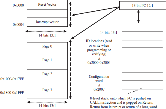
Figure 13.5 Program Memory Addresses for Reset, Interrupt Vectors and Pages 0, 1, 2 and 3
13.3.4 SFR Addresses in data memory
The lowest 32 B addresses in banks 0 and 1 and 16 B addresses in banks 2 and 3 are the SFRs addresses for the peripheral and IO control. 16 addresses between 0x70 and 0x7F are the same in all four banks. Figure 13.6 shows the distribution of space for the SFRs. Certain SFRs mirror in other bank-pair or in other banks.
Table 13.4 gives the meaning of symbols for the SFRs in bank 0. The table also specifies full form and 9-bit addresses of bytes at the SFRs (for IO control and peripherals). Direct addresses of 7-bit or indirect 8-bit addresses are used in PIC instructions.
TABLE 13.4 Special Function Registers at Bank 0
| Symbol | Full Form | 9-bit Address and Mirror Address (If Any) |
|---|---|---|
IndirectAddr (INDF) |
Invisible (not physical) Register 0a |
0x000 |
TMR0 |
Timer 0 time/count holding register |
0x001/0x081/0x101/0x181 |
PCL |
program counter lower byte |
0x002/0x082/0x102/0x182 |
STATUS |
status register |
0x003/0x083/0x103/0x183 |
FSR |
file select register |
0x004/0x084/0x104/0x184 |
PORTA |
6-bit PORTA input/output bits |
0x005 |
PORTB |
8-bit PORTB input/output bits |
0x006 and 0x106 |
PORTC, D |
8-bit PORTC, D input/output bits |
0x007,0x008 |
PORTE |
3-bit PORTA input/output bits |
0x009 |
PCLATH (PC address translation higher bits) |
PC higher 5-bits [bits b4-b3 corresponds to page number 0, 1, or 2 or 3] |
0x00A, 0x08A, 0x10A, 0x18A |
INTCON |
Interrupt control register |
0x00B, 0x08B, 0x10B, 0x18B. |
PIR1, PIR2 |
Peripheral Interrupt flags register 1, 2 |
0x00C, 0x00D |
TMR1L, TMR1H and T1CON |
Timer 1 time/count holding register lower and higher) and T1 control |
0x00E, 0x00F and 0x010 |
TMR2, T2CON |
Timer 2 time/count holding register, T2 control |
0x011 and 0x012 |
SSPBUF, SSPCON |
SSP Buffer and SSP control |
0x013-0x014 |
CCPR1L-CCPR1H |
CCP Register 1 lower and higher |
0x015-0x016 |
CCP1CON |
CCP1 control |
0x017 |
RCSTA |
Receiver status and control register bits for modes of serial port |
0x018 |
TxREG |
USART transmit data register |
0x019 |
RCREG |
USART receive data register |
0x01A |
CCPR2L-CCPR1H |
CCP Register 2 lower and higher |
0x01B-0x01C |
CCP1CON |
CCP2 control |
0x01D |
ADRESH |
AD result higher 2-bit |
0x011 |
ADCON0 |
AD control register 0 |
0x01F |
a When INDF is addressed the content of the FSR is used to address data memory (Example 13.25 will clarify it).

Example 13.11
Registers for CCP2 captured value from timer or CCP2 value for compare with timer or for PWM output are at registers CCPR2L-CCPR1H at address 0x01B and 0x01C.
Table 13.5 gives the SFRs that appear distinct for processor read and write at bank 1.
TABLE 13.5 Addresses for Read-cum-write PIC Special Function Registers at Bank 1
| Symbol | Full Form | 9-bit Address |
|---|---|---|
IndirectAddr(INDF) |
Invisible (not physical) Register 0 |
0x080 |
OPTION_REG |
Option register |
0x081, 0x181 |
PCL |
program counter lower byte |
0x02/0x82/0x102/0x182 |
STATUS |
status register |
0x03/0x83/0x103/0x183 |
FSR |
file select register |
0x04/0x84/0x104/0x184 |
TRISA |
6-bit transmit-receive input select register for PORTA input/output bits |
0x085 |
TRISB |
8-bit transmit-receive input select register for PORTB input/output bits |
0x086/0x186 |
TRISA C, D |
8-bit TRISC, D for input/output bits |
0x087 , 0x088 |
TRISE |
3-bit TRISE for input/output bits |
0x089 |
PCLATH |
PC higher 5-bits |
0x0A/0x8A/0x10A/0x18A |
INTCON |
Interrupt control register |
0x0B/0x8B/0x10B/0x18B. |
PIE1, PIE2 |
Peripheral Interrupt enable register 1, 2 |
0x08C, 0x08D |
PCON |
Power control register |
0x08E |
SSPCON2 |
SSP control2 |
0x091 |
PR2 |
Period register for timer 2 post scaling |
0x092 |
SSPADD-SSPSTAT, CCP1CON |
SSP address and SSP status register |
0x093-094 |
USART transmitter status register |
0x098 |
|
SPBRG |
SCI baud rate select register |
0x099 |
ADRESL |
AD result lower byte |
0x09E |
ADCON1 |
AD control register 1 |
0x09F |
Not used |
|
0x08F, 0x090, 0x095, 0x096, 0x097, 0x09A, 0x09B, 0x09C, 0x09D |
Example 13.12
- Assume that a byte is written at FSR. The FSR address is 0x84 in bank 1. It will also be accessible from bank 0, bank 2 and 3.
- AD lower byte is accessible from Bank 1 address 0x9E using 7-bit direct address 0x1E when RP1:RP0 are 01.
Table 13.6 gives the SFRs that appear at bank 2
TABLE 13.6 Special Function Registers at Bank 2
| Symbol | Full Form | 9-bit Address |
|---|---|---|
IndirectAddr(INDF) |
Invisible (not physical) Register 0 |
0x100 |
TMR0 |
Timer T0 |
0x101, 0x181 |
PCL |
program counter lower byte |
0x002/0x082/0x102/0x182 |
STATUS |
status register |
0x003/0x083/0x103/0x183 |
FSR |
file select register |
0x04/0x084/0x104/0x184 |
PORTB |
Port B input/output bits RB0 to RB7 |
0x105 |
PCLATH |
PC higher 5-bits |
0x00A/0x08A/0x10A/0x18A |
INTCON |
Interrupt control register |
0x00B/0x08B/0x10B/0x18B. |
EEDATA |
EE data lower byte |
0x10C |
EEADDR |
EE address lower byte |
0x10D |
EEDATH |
EE data higher bits |
0x10E |
EEADRH |
EE Address higher bits |
0x10F |
Not used |
Read as 0 |
0x105, 0x107, 0x108, 0x109 |
Table 13.7 gives the SFRs that appear at bank 3.
TABLE 13.7 Special Function Registers at Bank 3
| Symbol | Full Form | 9-bit Address |
|---|---|---|
IndirectAddr(INDF) |
Invisible (not physical) Register 0 |
0x080 |
OPTION_REG |
Option register |
0x081/0x181 |
PCL |
program counter lower byte |
0x002/0x82/0x102/0x182 |
STATUS |
status register |
0x003/0x083/0x103/0x183 |
FSR |
file select register |
0x004/0x084/0x104/0x184 |
8-bit transmit-receive input select register for PORTB input/output bits |
0x086/0x186 |
|
PCLATH |
PC higher 5-bits |
0x00A/0x08A/0x10A/0x18A |
INTCON |
Interrupt control register |
0x00B/0x08B/0x10B/0x18B. |
EECON1, EECON2 |
EEPROM control registers 1 and 2 |
0x18C, 0x18D |
Reserved |
Reserved Maintained as 0 |
0x18E and 0x18F |
Not used |
|
0x185, 0x187,0x188, 0x189 |
13.4 IO PORTS
PIC 16F877 has following IO features: There are five ports. PORTD also functions as Parallel Slave Port. Table 13.8 gives the meanings of the symbols used for the ports A to E, their data direction registers and PSP present in PIC family MCU version 16F877. It also gives the use of each one.
TABLE 13.8 The PORTs and Data Direction Registers in the Hardware Architecture and the Pins Used
| Symbol | Full Form | Use |
|---|---|---|
PORTA |
Bi-direction Port A RA0, RA1, RA2, RA3, RA4 and RA5 (All TTL except RA4). Data direction register sets I/O |
6-bit port for the inputs/outputs. PORTA also multiplexes with the multi-channel analog inputs, AN0, AN1, AN2, AN3, clock-input to timer TMR0 when counting and AN4. Analog inputs connect the internal ADC (Analog to Digital Converter). |
PORTB |
Bi-direction Port B RB0, RB1, RB2, RB3, RB4, RB5, RB6 and RB7 (All TTL ) and RB1, RB6 and RB7 (also ST). Data direction register sets data bits direction (I or O) |
8-bit port for the inputs/outputs, |
PORTC |
Bi-direction Port C RC0, RC1, RC2, RC3, RC4, RC5, RC6 and RC7 (All ST). I or O sets as data direction register |
8-bit port for the inputs/outputs, and peripherals when they are programmed for use. |
Bi-direction Port D RD0, RD1, RD2, RD3, RD4, RD5, RD6 and RD7 (Each TTL or ST) |
8-bit port for the inputs/outputs. PORTD also multiplexes with the PSP when a microprocessor bus is interfaced to the MCU. |
|
PORTE (or control signals |
Bi-direction Port E RE0, RE1, RE2, (Each TTL or ST) |
3-bit port for the inputs/outputs. PORTE also controls the PSP when a microprocessor bus is interfaced to the MCU. |
TRISA |
Data -direction Register for Port A RA0, RA1, RA2, RA3, RA4 and RA5 pins |
• RA0 is input when bit b0 of TRISA is 1 and is output when 0. |
TRISB |
Data direction register for Port B |
• RB0 is input when bit b0 of TRISB is 1 and is output when 0. |
TRISC |
Bi-direction Port C |
• RC0 is input when bit b0 of TRISC is 1 and is output when 0. |
TRISD |
Bi-direction Port D RD0, RD1, RD2, RD3, RD4, RD5, RD6 and RD7 |
• RD0 is input when bit b0 of TRISD is 1 and is output when 0. |
TRISE /PSP status/ control bits |
Bi-direction Port E RE0, RE1, RE2 pins control and Parallel Slave Port SP status/ control bits |
• RE0 is input when bit b0 of TRISE is 1 and is output when 0. |
a ST stands for Schmitt trigger input. It means when input voltage is rising then the 1 is latched when that is 0.66 of VDD and when input voltage is falling then the 0 is latched when that 0.33 of VDD. ST enables edge triggering (sharp transitions to 1 or 0 at the threshold + or −).
PORTA Address 0x05H in bank 0 has 6 bits (RA0 to RA5). RA0 to RA5 pins also function as four analog input channels AN0 to AN4. Pins RA3 and RA2 also used to provide V+ref and V−ref . When AD is not used, RA pins accept digital input bits and send digital output also. TRISA bits 0 to 5 decides the direction input or output at an RA pin. Pin RA4 is also used as T0CKI (timer 0 clock input).
PORTE Address 0x09 in bank 0 has 3 bits (RE0 to RE2). RE0 to RE2 pins also function as three analog input channels AN5 to AN7. Pins RE0, RE1 and RE2 also provide ![]() ,
, ![]() and
and ![]() control signals when PSP is used. When AD or PSP is not used, RE pins accept digital input bits and send digital output also. TRISE bits 0 to 2 (address 0x89) decide the direction input or output at an RE pin.
control signals when PSP is used. When AD or PSP is not used, RE pins accept digital input bits and send digital output also. TRISE bits 0 to 2 (address 0x89) decide the direction input or output at an RE pin.
PORTB Address 0x06/0x106 in bank 0/2 has 8 bits (RB0 to RB7). RB0, RB3, RB6 and RB7 also provide the INT (external interrupt), PGM, PGC and PGD (programming serial clock and data) signals when these functions are enabled. RB pins accept the digital input bits and send digital output also. TRISB bits 0 to 7 (address 0x86/0x186) decide the direction input or output at an RB pin.
PORTC Address is 0x07 in bank 0 and has 8 bits (RC0 to RC7). RC0 to RC7 pins also function as timer 1, SPI and USART (SCI) signals. Pins RC6, RC7 are also used as SCI synchronous/asynchronous in/out. RC5, RC4, RC3 provide SDO, SDI/SDA, SCK/SCL signals for the SPI/I2C mode communication. RC0 and RC1 are used by T1 and CCP2 signals. RC pins accept digital input bits and send digital output also. TRISC bits 0 to 7 (address 0x87) decide the direction input or output at an RC pin.
PORTD/PSP Address 0x08 in bank 0 has 8 bits (RD0 to RD7). RD0 to RD7 pins also function for the parallel slave port (PSP) pins PSP0 to PSP7. When PSP function disabled, the RD pins accept digital input bits and send digital output also. TRISD bits 0 to 7 (address 0x88) decide the direction input or output at individual RD pins. When PSP is used, the read or write function at RD0 to RD7 pins is controlled by ![]() (RE0) or
(RE0) or ![]() (RE1) signals provided
(RE1) signals provided ![]() (RE2) is active.
(RE2) is active.
13.4.1 Serial Ports— MSSP and USART
MSSP (Master synchronous serial port) has two functions: SPI and I2C. Figure 13.7 shows the MSSP ports. USART has two functions: synchronous-communication and asynchronous-communication using the SCI. Figure 13.8 shows the USART port signals in SCI. When using a serial communication interface (SCI), then RC7 and RC8 interface as the data and clock during the serial synchronous-communication. When using serial communication interface (SCI), the RC7 and RC8 interface as the TxD and RxD during the asynchronous communication.


Figure 13.8 USART Ports for synchronous and asynchronous communication in PIC16F877
Table 13.9 gives the meanings of the symbols used for the SCI (USART) and SPI/I2C serial communication in PIC family MCU version 16F877. It also gives the use of each one.
TABLE 13.9 SCI (USART) and SPI/I2C Serial Communication in PIC Family MCU Version 16F877
| Symbol | Full Form | Use |
|---|---|---|
MSSP [Two modes: SPI (serial peripheral interface) and I2C] |
Master Synchronous Serial Interface Port for communicating with other peripheral (serial EEPROMs, shift registers, display drivers, AD etc) or MCU |
• SPI mode has 8-bit serial data synchronously out and simultaneously synchronously in at pins SDO and SDI. Serial clock SCK pin gives synchronising clock output. An optional 4th pin is used as SS (Slave select, when 0 then functions SPI functions as slave). SCK is input in slave mode. |
USART (Addressable universal synchronous/ asynchronous receiver transmitter) using Serial Communication Interface (SCI) [Associates SPBRG, RCSTA and TXSTA] |
• Full duplex for serial asynchronous communication to CRT terminal or personal computer. |
13.5 TIMERS AND CCP DEVICES
PIC MCU has two 8-bit timers—timer TMR2 and timer TMR0, and has one 16-bit timer TMR1. TMR1 [16-bit timer/ counter] can be used for the compare outputs and input captures in conjunction with two CCP devices, CCP1 and CCP2. PIC MCU has the OST, PWRT and WDT timers also.
Table 13.10 gives the meanings of the symbols used in the Figure 13.2 and Tables 13.4, 13.5 and 13.6 for the timer subunits, devices and SFRs in 16F877. It also gives the use of each one.
TABLE 13.10 The Subunits in the Hardware Timers, CCPs, OST, PWRT and WDT and the Uses
| Symbol | Full Form | Use |
|---|---|---|
Timer0 |
Timer TMR0 [Associates with TMR0, INTCON (interrupt control) and OPTION_REG (option register) registers] |
• 8-bit internal timing/counting device, which can be loaded (written) or read. It has programmable prescaler for CLKOUT inputs to it. |
Timer1 |
Timer TMR1 [Associates with TMR1L (holding register lower byte), TMR1H (holding register higher byte), INTCON (interrupt control), T1CON (TMR1 control), PIR1 (peripheral interrupt flags register!) and PIE1 (peripheral interrupt enable register1) |
• 16-bit internal timing/counting device, which can be loaded (written) or read. The clock inputs are at fOSC/4 (Oscillator frequency divided by 4). It has programmable prescaler (1 or 2 or 4 or 8) for timer inputs to it. |
Timer TMR2 [Associates with TMR2 (T2 holding register), INTCON (interrupt control), T2CON (TMR2 control), PR2 (T1 period register) PIR1 (peripheral interrupt fl ags register) and PIE1 (peripheral interrupt enable register1) |
• 8-bit internal timing/counting device, which can be loaded (written) or read. The clock inputs are at fOSC/4 (Oscillator frequency divided by 4). It has programmable prescaler (1 or 4 or 16) for timer inputs to it. |
|
CCP1, 2 |
Capture/Compare/ PWM devices 1 and 2. [Identical except special event trigger.] (Six combinations of CCP1, 2 are Capture, capture or Capture, Compare, Compare/ Compare, Compare/ Compare, PWM/PWM, PWM/Capture, PWM/ Compare) |
• Two 16-bit internal devices (each device has 16-bit register, which can function as either 16-bit capture register or 16-bit compare register or PWM Master or Slave duty cycle register) using the timers. |
Watchdog timer |
• CONFIG_REG (WDTE watchdog timer enables by bit b2 = 1). |
|
OST |
Oscillator Start-up Timer |
• It provides 1024 oscillation cycles delay after PWRT time-out. It is for let oscillator stabilise after the oscillations start. |
PWRT |
o Power-up timer |
• There is a 72 ms time-out on power-up and power-on reset. 72 ms is internally set by internal oscillator circuit with internal RC. |
13.5.1 Timers 0, 1 and 2
(a) Timer TMR0 We can select internal or external clock (through RA4 pin) for incrementing counts in the TMR0 holding register. When using a 20 MHz crystal, the counter inputs are at the periodic intervals of 0.2 μs (200 ns) = 1 instruction cycle time.
Prescaling can be done on selecting the PS2:PS0 bits in OPTION_REG option register at address 0x81/0x181. PS2-PS0 can have values 0 (000) to 7 (111). The prescaling factor can be set as 20 or 21, …or 27. Prescaling can be used either by TMR0 or WDT at an instance. Figure 13.9 shows TMR0 inputs and functioning.
TMR0 holding register is read or written from address 0x01 or 0x101.
Example 13.13
- TMR0 SFR at an instance is read and is equal to 0x7F. Assume that it is read again after 32 periodic clock inputs of intervals of 200 ns and prescaling factor is set at 16. What will be the value in TMR0?
0d127 + 32 ÷ 16 = 0d129 = 0x81.
- After how much time will it generate the overflow interrupt, and the interrupt flag will set if at the beginning TMR0 = 0x80.
The overflow will occur after (0xFF− 0x80) increments of the TMR0. Then 128 × 16 × 200 ns = 409.6 μs will be the time after which overflow interrupt will occur and the overflow flag will set.
(b) Timer TMR2 We can select the internal clock for incrementing counts in the TMR2 holding register. When using a 20 MHz crystal, the counter inputs are at periodic intervals of 0.2 μs (200 ns) = 1 instruction cycle time. TMR2 holding register is read or written using address 0x11.

Figure 13.9 Timer TMR0 Inputs and Functioning in PIC16F877
Prescaling can be done on selecting the T2CKPS1:T2CKPS0 bits in T2CON register at address 0x12. The bits when = 00 the prescaler factor p = 1, when = 01 then p is 4 and when = 10 or 11, p is 16.
TMR2 has post scaling features also. Four TOUTPS4:TOUTPS0 bits in T2CON register can take values from 0000 to 1111 ( 0 to 15), then the post scaling factor can be set from 1 to 16 (one plus the value of 4 bits). Figure 13.10 shows TMR2 inputs and functioning.
There is a register PR2 at address 0x92. The contents of PR2 and TMR2 when becomes equal then the TMR2 interrupt flag is set on first such instance if post scaling factor q = 1 and set on 8th such instance if q = 8. The interrupt will also be generated if TMR2 interrupt is enabled. TMR2 can be used as time base for PWM mode of the CCP1, 2.
Example 13.14
- TMR2 SFR at an instance is read and is equal to 0x7F. Assume that it is read again after 32 periodic clock inputs of intervals of 200 ns and the prescaling factor is set at 8. What will be the value in TMR0?
0d127 + 32 ÷ 8 = 0d131 = 0x83.
- Assume prescaling factor is set at 4. Assume post scaling factor = 8 and PR2 is written 0x3F. After how much time will it generate overflow interrupt and the interrupt flag will set if at the beginning TMR2 = 0x00.
The overflow will occur on 8th time compare and match of the TMR2 with PR2. The TMR2 increments from 0x00 to 0x3F and then increments to 0x40 in 64 × 4 × 200 ns and the TMR2 resets if post scaling factor = 1. When post scaling factor = 8, then 8th match will occur in 64 × 4 × 200 × 8 ns. Therefore, the overflow interrupt will occur and overflow flag will set in 64 × 4 × 200 × 8 ns = 0.409600 ms.
(c) Timer TMR1 We can select internal clock or external for incrementing counts in the 16-bit TMR1 holding registers TMR1H-TMR1L at addresses 0x0F-0x0E. When using a 20 MHz crystal, the counter internal clock inputs are at the periodic intervals of 0.2 ms (200 ns) = 1 instruction cycle time. TMR1 holding register higher and lower bytes are read or written from addresses 0x0F-0x0E.
We can also select the oscillator input for TMR1. The oscillator is built-in. It is a low-power oscillator. It can oscillate up t0 200 kHz.
Prescaling can be done on selecting the T1CKPS1:T1CKPS0 bits in T1CON register at address 0x10. The bits 00 makes prescaler factor = 1, 01 then factor is 2 and when 10 then factor is 4 or when 11 the factor is 8. Figure 13.11 shows TMR1 inputs and functioning.
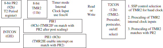
Figure 13.10 Timer TMR2 Inputs and Functioning in PIC16F877

TMR1 has an internal rest feature. It can be generated by one of the two CCP1, 2. A CCP can generate special event trigger when CCP1M3:CCP1M0 = 1011, then the comparison match will generate the signal and special event trigger.
Example 13.15
TMR1H-TMR1L SFRs at an instance are read and the 16-bits are equal to 0xFFE0. Assume that it is read again after 32 periodic clock inputs of intervals of 200 ns and the prescaling factor is set at 1. What will be actions after 32 periodic clock inputs?
The holding register bits = 0xFF80 + 0x20 ÷ 0x01 = 0x0000 as TMR1H-TMR1L can hold only 16-bits. There will be overflow interrupt TMR2I. The TMR2IF flag will be set.
13.5.2 Compare Outputs and Interrupts Using CCP1 and CCP2
One of the modes is the compare mode of CCP1 (compare/Capture/PWM peripheral device 1) and CCP2 (compare/Capture/PWM peripheral device 2).
Figure 13.12 shows compare mode functioning in PCI16F877.
CCP1 Compare Mode
16-bit in compare mode of CCP1 are CCPR1H: CCPR1L, written and read using address 0x16 and 0x15 (bank 0 SFRs). CCP1 control register is CCP1CON. It is written or read using 0x17H [Table 13.4].

Figure 13.12 CCP1 Compare Mode Functioning in PIC16F877
Consider 16-bit timer TMR1. The time/counts at the holding register of TMR1 are 16-bits at TMR1H:TMR1L. They are at address 0x0F-0x0E. The bits are used for comparing and matching the 16-bits at CCPR1L:CCPR1H by the CCP1 device when CCP1 compare mode is enabled.
CCP1CON bits at 0x17 are used as follows:
Bit b7-b6 are always 0 (not implemented in 16F877) and Bit b5-b4 are not used in compare mode.
Bit b3-b2-b1-b0 = 1111 then compare/capture/PWM mode is disabled. Where = 1000 then on compare output set mode is activated. CCP1 device sets an output on match (means TMR1H:TMR1L counts have become equal to CCPR1L:CCPR1H). A flag CCP1IF (CCP1 interrupt flag) is also set. The output is at pin CCP1 (pin RC2 of PORTC).
If bits = 1001 then on compare output clear mode is activated. CCP1 device clears the output on match (means TMR1H:TMR1L counts have become equal to CCPR1L:CCPR1H). A flag CCP1IF (CCP1 interrupt flag) is also set. The output is at pin CCP1 (pin RC2 of PORTC).
If bits = 1010 then the compare mode software timer mode is activated. CCP1 device generates software interrupt match (means TMR1H:TMR1L counts have become equal to CCPR1L:CCPR1H). A flag CCP1IF (CCP1 interrupt flag) is also set. The output at pin CCP1 (pin RC2 of PORTC) is not changed.
If bits = 1011 then the compare mode special event trigger mode is activated. CCP1 device generates reset for TMR1 on match (means TMR1H:TMR1L counts have become equal to CCPR1L:CCPR1H). A flag CCP1IF (CCP1 interrupt flag) is also set. The output at pin CCP1 (pin RC2 of PORTC) is not changed.
CCP1IF (CCP1 interrupt flag) is in SFR PIR1 (peripheral interrupt register 1) bit b2. PIR1 address is 0x0C. When CCP1IF (CCP1 interrupt flag) is set, the interrupt service routine executes if interrupt is enabled in SFR PIE1 (peripheral interrupt enable register 1) bit b2 and INTCON PEIE (peripheral-enable interrupts enable) bit b6. PIE1 address is 0x8C. INTCON address is 0x0B/0x8B/0x10B/0x18B.
CCP2 Compare Mode
16-bit in compare mode of CCP2 are CCPR2H:CCPR2L, written and read at address 0x1C and 0x1B (bank 0 SFRs). CCP2 control register is CCP1CON. It is written or read using 0x17H [Table 13.4].
The time/counts at the holding register of TMR1 are 16-bits at TMR1H:TMR1L. They are at address 0x0F-0x0E. The bits are also used for comparing and matching the 16-bits at CCPR2L:CCPR2H by the CCP2 device when CCP2 compare mode is enabled.
CCP2CON bits at 0x1D are used as follows:
Bit b7-b6 are always 0 (not implemented in 16F877), Bit b5-b4 are not used in the compare mode. Bit b3-b2-b1-b0 = 1111 then compare/capture/PWM mode disabled. If = 1000 then on compare set output mode is activated. CCP2 device sets an output on match (means TMR1H:TMR1L counts have become equal to CCPR2L:CCPR2H). A flag CCP2IF (CCP2 interrupt flag) is also set. The output is at pin CCP2 (pin RC1 of PORTC).
If bits = 1001 then on compare clear output mode is activated. CCP2 device clears the output on match (means TMR1H:TMR1L counts have become equal to CCPR2L:CCPR2H). A flag CCP2IF (CCP2 interrupt flag) is also set. The output is at pin CCP2 (pin RC1 of PORTC).
If bits = 1010 then the software timer mode of compare option is activated. CCP2 device generates software interrupt match (means TMR1H:TMR1L counts have become equal to CCPR2L:CCPR2H). A flag CCP2IF (CCP2 interrupt flag) is also set. The output at pin CCP2 (pin RC1 of PORTC) is not changed.
If bits = 1011 then on compare the special event trigger mode is activated. CCP2 device starts AD conversion if ADC device is activated. CCP2 device generates reset for TMR1 on match (means TMR1H:TMR1L counts have become equal to CCPR2L:CCPR2H). A flag CCP2IF (CCP2 interrupt flag) is also set. The output at pin CCP2 (pin RC1 of PORTC) is not changed.
CCP2F (CCP1 interrupt flag) is in SFR PIR2 (peripheral interrupt register 2 bit b0. PIR2 address is 0x0D. When CCP2IF (CCP2 interrupt flag) is set, the interrupt service routine executes if interrupt is enabled by in SFR PIE2 (peripheral interrupt enable register 2) bit b0 and INTCON PEIE (peripheral-enable interrupts enable) bit b6. PIE2 address is 0x8D. INTCON address is 0x0B/0x8B/0x10B/0x18B.
Consider the following example as to why we need output comparison unit.
Example 13.16
Assume that a running counter TMR1 is running and incrementing after every 0.2 μs (200 ns) instruction cycle time. Assume that four actions are to be initiated when its contents are 0x1000, 0x2000, 0x4000 and 0x8000 so that actions takes place at time values T = 4096 × 0.2 μs, 8192 × 0.2 μs, 16384 × 0.2 μs and 32768 x 0.2 μs. Assume that action 1 requires RC2 pin output become = 0 and action 2 requires AD conversion start. Action 3 requires that RC1 pin out put = 0. Action 4 requires the RC2 pin output to become 1. One method can be used to read the TMR1 SFR values continuously.
- when (T ≡ 4096) Action 1 by running ISR1
- when (T ≡ 8192) Action 2 by running ISR2
- when (T ≡ 16384) Action 3 by running ISR3
- when (T ≡ 32768) Action 4 by running ISR2
However, suppose AD conversion is over and the MCU is executing ISR_AD after end of conversion. TMR1 counts become equal to 16384 at that instance. Then action 3 will be delayed till there is return for from ISR_AD.
CCP1 and CCP2 of PIC compare mode functions give a way to solve the problem of actions with least delays in the presence of the interrupt service latencies. [Interrupt service latency means time delay between occurrence of interrupt (setting of the interrupt flag) and start of the ISR for the interrupt. The latency is due to context switching time and due to presently executing service routine of higher priorities than the present interrupt.]
The programming is done as follows:
Step 1: Write CCP1H:CCP1L = 4096 and CCP2H:CCP2L = 8192 (because CCP2 special event trigger mode initiates the AD conversion also and that is required for action 2 when TMR1 = 8192).
Step 2: Program CCP1CON control bits = 1001 because action 1 is to clear the pin RC2 output. Enable CCP1 device. When CCP1H:CCP1L = TMR1H:TMR1L = 4096 then action 1 takes place and RC2 = 0.
Step 3: Program CCP2CON control bits = 1011 because action 2 is to start the AD conversion. Enable CCP2 device.
Step 3: Since, action 2 also resets the TMR1 to 0x0000. Therefore, the ISR which executes on CCP2 compare interrupt writes the CCP2 = 16384 − 8192= 8192, as 8192 × 0.2 μs is already over till action 2. CCP2 is written because action 3 is to be on RC1 CCP2 pin. Enable CCP2 device. Program CCP2CON control bits = 1000 because action 3 is to set the RC1 CCP2 pin output.
Step 4: Since, the action 3 also does not reset the TMR1 to 0x0000, therefore the ISR which executes on CCP2 compare interrupt for action 2, also writes the CCP1 = 32768 − 8192 as 8192 × 0.2 μs is already over till action 2. CCP1 is written because action 4 is to be on RC2 CCP1 pin. Enable CCP1 device. Program CCP1CON control bits = 1000 because action 3 is to set the RC2 CCP1 pin output =1.
13.5.3 Software Timer Interrupts Using CCP1 and CCP2
Two software timers are programmable by CCP1CON and CCP2CON (lower 4-bits in each of them are programmed). Software timer interrupts do not generate a pin output on successful comparison. It generates a software timer interrupt when CCP1 control bits b3-b2-b1-b0 are set at 1010 and another interrupt when CCP2 control bits b3-b2-b1-b0 are set at 1010.
13.5.4 Input Captures Using CCP1 and CCP2
On an event, a signal may be generated (1 or 0). As soon as the input signal occurs, the timing instance needs to be captured in some register. When an event occurs, we have to find the instance of time at which the event occurred. Time is noted from the TMR1 running counter. Additional feature in PIC is that there are two CCP devices, CCP1 and CCP2. They can be programmed to function in capture modes. Figure 13.13 shows capture mode functioning.
There is 16-bit timer TMR1. The time/counts at the holding register of TMR1 are 16-bits at TMR1H:TMR1L. They are at address 0x0F-0x0E. The bits are used for capturing into the CCPR1L:CCPR1H by the CCP1 device when CCP1 capture mode is enabled and CCP1pin (RC2) receives the input edge.
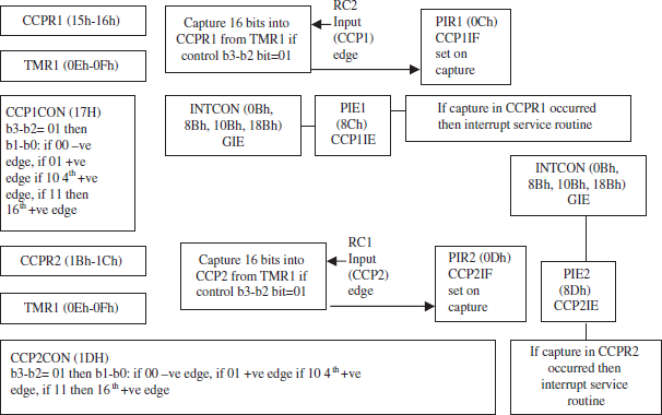
Figure 13.13 CCP1 Capture Mode Functioning in PIC16F877
The time/counts at the holding register of TMR1 are 16-bits at TMR1H:TMR1L. They are at address 0x0F-0x0E. The bits are used for capturing into the CCPR2L:CCPR2H by the CCP2 device when CCP2 capture mode is enabled and CCP2 pin (RC1) receives the input edge.
CCP1 Capture Mode
One of the modes is capture mode for CCP1 (compare/Capture/PWM peripheral device 1) as well as CCP2 (compare/Capture/PWM peripheral device 2).
16-bit in capture mode of CCP1 are CCPR1H: CCPR1L, written and read using address 0x16 and 0x15 (bank 0 SFRs). CCP1 control register is CCP1CON. It is written or read using 0x17H [Table 13.4]. CCP1CON bits at 0x17 are used as follows:
Bit b7-b6 are always 0 (not implemented in 16F877), Bit b5-b4 are not used in capture mode.
Bit b3-b2-b1-b0 = 1111 then compare/capture/PWM mode disabled. If = 0100 then the capture mode is activated. CCP1 device captures a falling edge input (1 to 0 transition) at RC2 CCP1 pin and writes on capture (means 16-bits for the TMR1H:TMR1L counts are written at CCPR1L:CCPR1H). A flag CCP1IF (CCP1 interrupt flag) is also set. The capture is at pin CCP1 (pin RC2 of PORTC).
If bits = 0101 then the capture mode is activated. CCP1 device captures a rising edge input (1 to 0 transition)at RC2 CCP1 pin and writes on capture (means 16-bits for the TMR1H:TMR1L counts are written at CCPR1L:CCPR1H). A flag CCP1IF (CCP1 interrupt flag) is also set. The capture is at pin CCP1 (pin RC2 of PORTC).
If bits = 0110 then the capture mode is activated. CCP1 device captures a every 4th rising edge (0 to 1 transition) input at RC2 CCP1 pin and writes on capture (means 16-bits for the TMR1H:TMR1L counts are written at CCPR1L:CCPR1H). A flag CCP1IF (CCP1 interrupt flag) is also set. The capture is at pin CCP1 (pin RC2 of PORTC).
If bits = 0111 then the capture mode is activated. CCP1 device captures a every 16th rising edge (0 to 1 transition) input at RC2 CCP1 pin and writes on capture (means 16-bits for the TMR1H:TMR1L counts are written at CCPR1L:CCPR1H). A flag CCP1IF (CCP1 interrupt flag) is also set. The capture is at pin CCP1 (pin RC2 of PORTC).
CCP1IF (CCP1 interrupt flag) is in SFR PIR1 (peripheral interrupt register 1) bit b2. PIR1 address is 0x0C. When CCP1IF (CCP1 interrupt flag) is set, the interrupt service routine executes if interrupt is enabled by in SFR PIE1 (peripheral interrupt enable register 1) bit b2 and INTCON PEIE (peripheral-enable interrupts enable) bit b6. PIE1 address is 0x8C. INTCON address is 0x0B/0x8B/0x10B/0x18B.
CCP2 Capture Mode
16-bit in capture mode of CCP2 are CCPR2H:CCPR2L, written and read at address 0x1C and 0x1B (bank 0 SFRs). CCP2 control register is CCP1CON. It is written or read using 0x17H [Table 13.4].
CCP2CON bits at 0x1D are used as follows:
Bit b7-b6 are always 0 (not implemented in 16F877), Bit b5-b4 are not used in capture mode.
Bit b3-b2-b1-b0 = 1111 then compare/capture/PWM mode disabled. If t = 0100 then the capture mode is activated. CCP2 device captures a falling edge input (1 to 0 transition)at RC1 CCP2 pin and writes on capture (means 16-bits for the TMR1H:TMR1L counts are written at CCPR2L:CCPR2H). A flag CCP2IF (CCP2 interrupt flag) is also set. The capture is at pin CCP1 (pin RC2 of PORTC).
If bits = 0101 then the capture mode is activated. CCP2 device captures a rising edge input (1 to 0 transition)at RC1 CCP1 pin and writes on capture (means 16-bits for the TMR1H:TMR1L counts are written at CCPR2L:CCPR2H). A flag CCP2IF (CCP2 interrupt flag) is also set. The capture is at pin CCP2 (pin RC1 of PORTC).
If bits = 0110 then the capture mode is activated. CCP2 device captures a every 4th rising edge (0 to 1 transition) input at RC21 CCP2 pin and writes on capture (means 16-bits for the TMR1H:TMR1L counts are written at CCPR1L:CCPR1H). A flag CCP2IF (CCP2 interrupt flag) is also set. The capture is at pin CCP2 (pin RC1 of PORTC).
If bits = 0111 then the capture mode is activated. CCP2 device captures a every 16th rising edge (0 to 1 transition) input at RC2 CCP2 pin and writes on capture (means 16-bits for the TMR1H:TMR1L counts are written at CCPR2L:CCPR2H). A flag CCP2IF (CCP2 interrupt flag) is also set. The capture is at pin CCP2 (pin RC1 of PORTC).
CCP2F (CCP1 interrupt flag) is in SFR PIR2 (peripheral interrupt register 2 bit b0. PIR2 address is 0x0D. When CCP2IF (CCP2 interrupt flag) is set, the interrupt service routine executes if interrupt is enabled by in SFR PIE2 (peripheral interrupt enable register 2) bit b0 and INTCON PEIE (peripheral-enable interrupts enable) bit b6. PIE2 address is 0x8D. INTCON address is 0x0B/0x8B/0x10B/0x18B.
Consider Example 13.17 to determine why an output comparison device is done.
Example 13.17
Assume that a running counter TMR1 is running and incrementing after every 0.2 μs (200 ns) instruction cycle time. Assume that three timing instances are to be found out for the 4th rising edge from source 1 and 1st and 16th falling edge from source 2. One method can be to read continuously the TMR1 SFR and the input edges generate the external interrupts at the port.
- When external interrupt 1 on 1st falling edge occurs then run ISR1 and read TMR1H:TMR1L.
- When external interrupt 2 on 4th rising edge occurs then run ISR2 and read TMR1H:TMR1L.
- When external interrupt 3 on 16th falling edge occurs then run ISR3 and read TMR1H:TMR1L.
However, suppose some service routine is executing when the 1st falling edge occurs. The timer reading will be delayed unless that all other interrupts are disabled when falling edge is to be detected and timing instance is to be noted.
CCP1 and CCP2 of MCU PIC capture mode functions give a way of solving the problem of actions with least delays in the presence of the interrupt service latencies. [Interrupt service latency means time delay between occurrence of interrupt (setting of the interrupt flag) and start of the ISR for the interrupt. The latency is due to context switching time and due to presently executing service routine of higher priorities than the present interrupt.]
The programming is done as follows:
Step 1: Give input from source 1 to RC2 CCP1. Program CCP1 for capture mode. Program CCP-1CON control bits = 0110 because the action 1 is to get the timing instance for the 4th rising edge from source 1. Enable CCP1 device. When 4th edge appears, the CCP1H:CCP1L captures 16-bits from = TMR1H:TMR1L. An ISR is run on the interrupt, the timing instance of action1 source 1 is saved at 0x71-0x72 by MOV instruction for register 0x15 (CCP1RH) to RAM 0x71 and register 0x16 (CCP1RH) to 0x72.
Step 2: Defined number of falling edge counts at 0x70 internal RAM. This is because there is no control bit to capture on 16th falling edge. (There are control bits to capture on 16th rising edge not on 16th falling edge.)
Step 3: Give input from source 2 to RC1 CCP2. Program CCP2 for capture mode. Program CCP-2CON control bits = 0100 because action 2 is to get the timing instance for the 1st falling edge from source 2.
Step 4: Enable CCP2 device and enable CCP interrupts. When 1st falling edge appears, the CCP2H:CCP2L captures 16-bits from = TMR1H:TMR1L. CCP2IF flag sets. CCP2I interrupt occurs and an ISR is executed to increment by 0x01 the edge-count parameter at the RAM 0x70. The ISR then saves the timing instance of action 2 source 2 is saved at 0x73-0x74 by MOV instruction for register 0x1B (CCP2RH) to RAM 0x73 and register 0x1C (CCP2RH) to 0x74 if 0x70 = 0x1.
Step 5: Repeat step 4 till falling edge counts 0x70 are less or equal to 0x0F. When 0x70 contents are 0x10 (=16), then the ISR then saves the timing instance of action 3 source 3 is saved at 0x75-0x76 by MOV instruction for register 0x1B (CCP2RH) to RAM 0x75and register 0x1C (CCP2RH) to 0x76.
13.5.5 Pulse Width Modulated Output
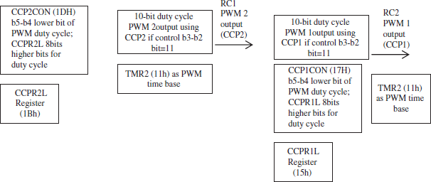
CCP1 and CCP2 can also control the PWM outputs. A PWM output enables at RC1/CCP2 pin and another at RC2/CCP1 pin. PWM resolution is 10 bit. One of the modes is PWM for CCP1 (compare/Capture/ PWM peripheral device 1) as well as CCP2 (compare/Capture/PWM peripheral device 2). PWM output means the pulses of period proportional to the bits in a register used for generating the PWM outputs. Figure 13.14 shows PWM functions of CCP1. Following example explains PWM action:
Example 13.18
- Assume that a running timer T is running and incrementing every 200 ns. A register is written 10 bits 10 0000 0000 [= 512]. When the T resets and starts then counts in T are x = 0. At that instance let an output = 1 and when x = 10 0000 0000, then that output becomes 0 and remains 0 till the timer overflows. It means that output = 1 for 512 × 200 ns and 0 for (1024 − 512) × 200 ns. The duty cycle of the output pulse = 512/1024 × 100% = 50%. Duty cycle period = 512 × 200 ns. Pulse period = 1024 × 200 ns.
- Now the register is written ten bits 01 0000 0000 [=256]. When the T resets and starts then counts x = 0000000000. At that instance let the output = 1 and when x = 01 0000 0000.then that output becomes 0 and remains 0 till the timer overflows. It means that output = 1 for 256 × 200 ns and 0 for (1024 − 512) × 200 ns. The duty cycle of the output pulse = 256/1024 × 100% = 25%. Duty cycle period = 256 × 200 ns. Pulse period = 1024 × 200 ns.
- If register is written value = pw, then output pulse duty cycle = (pw/1024) × 100%.
- The output is called PWM output. The output pulse is modulated as per the p bits. PWM output can be integrated by an external circuit to get the analog output proportional to pw. Duty cycle period = pw × 200 ns. Pulse period = 1024 × 200 ns.
8-bits out of 10-bits for the PWM mode of CCP1 are at CCPR1L and that copies to CCPR1H on reset. CCPR1L is written and read using address 0x15 (bank 0 SFR). CCPR1H is read only in PWM mode. The address is 0x16 (bank 0 SFR). CCP1 control register is CCP1CON. It is written or read using 0x17H [Table 13.4].
8-bits out of 10-bits for the PWM mode of CCP2 are at CCPR2L and that copies to CCPR2H on reset. CCPR2L is written and read using address 0x1B (bank 0 SFR). CCPR2H is read only in PWM mode. The address is 0x1C (bank 0 SFR). CCP2 control register is CCP2CON. It is written or read using 0x1DH [Table 13.4].
A PWM output has a time-base period (pulse-period) and PWM pulse frequency = 1/pulse-frequency.
There is 8-bit timer TMR2. The time/counts at the holding register of TMR2 are 8-bits at TMR2. PWM mode makes the TMR2 effectively function as 10-bit timer because 8-bit timer is concatenated with 2-bit internal prescaler (Q-clock). There is internal Q clock and RS latch for the PWM output from TMR2. TMR2 holding register is at address 0x11 and TMR2CON control register for TMR2 is at address 0x12. The bits are used for PWM period are the bits at PR2. PR2 address is 92H. Let PR2 be written as y. Let prescale factor = p. Tosc is the period of the oscillator.
The PWM period = [y + 1] × 4 × Tosc × p.
CCP1 PWM Mode
- PWM duty cycle 8 bits are written at CCPR1L and 2 bits are written at CCP1CON bits b5-b4. CCPR1H is internally loaded from CCPR1L at the reset of TMR2. There is thus double buffering of PWM duty cycle 8-bits. PWM mode makes CCPR1H as read only register.
- PWM period is written in PR2 register and TMR2 prescale value.
- Enable TMR2 by writing T2CON.
- CCP1 Pin is made output by clearing bit b2 of TRISC (data direction register for port C).
CP1CON is address 0x17 CCP1CON bits at 0x17 are used as follows:
Bit b7-b6 are always 0 (not implemented in 16F877) Bit b5-b4 are not used in PWM mode.
Bit b3-b2-b1-b0 = 11xx then compare/capture mode disabled. and PWM mode enabled Bit b5-b4 are lower two bits for the 10-bit PWM duty cycle.
PWM duty cycle period = (10-bits b5-b4 in CCP1CON-CCPR1L) × Tosc × TMR2 prescaler factor.
The bits are used for PWM period are the bits at PR2. PR2 address is 92H. Let PR2 be written as y. Let prescale factor = p. Tosc is the period of the oscillator.
The PWM time-base period = [y + 1] × 4 × Tosc × p.
When TMR2 = PR2, then on next increment oosfc TMR2 (i) TMR2 resets, (ii) CCP1 pin at RC2 = 1. If PWM duty cycle = 0%, then CCP1 pin is not set. (iii) 8-bits of PWM duty cycle value are latched into CCPR1H from CCPR1L. The time/counts at the holding register of TMR2 are 10-bits at TMR2 + internal prescaler bits. TMR2 8-bits are at address 0x11H. The bits are used for comparing and matching the 10-bits at 2-bits at b5-b4 in CCP1CON and 8-bits in CCPR1H by the CCP1 device when CCP1 PWM mode is enabled.
The interrupt service routine executes if interrupt is enabled by in SFR PIE1 (peripheral interrupt enable register 1) bit b2 CCP1IE and INTCON PEIE (peripheral-enable interrupts enable) bit b6. PIE1 address is 0x8C. INTCON address is 0x0B/0x8B/0x10B/0x18B. There is no interrupt flag in PWM mode.
CCP2 PWM Mode
- PWM duty cycle 8 bits are written at CCPR2L and 2 bits are written at CCP2CON bits b5-b4. CCPR2H is internally loaded from CCPR2L at the reset of TMR2. There is thus double buffering of PWM duty cycle 8-bits. PWM mode makes CCPR2H as read only register.
- PWM period is written in PR2 register and TMR2 prescale value.
- Enable TMR2 by writing T2CON.
- CCP2 Pin is made output by clearing bit b1 of TRISC (data direction register for port C).
CCP2CON is address 0x1D. CCP2CON bits at 0x1D are used as follows:
Bit b7-b6 are always 0 (not implemented in 16F877).
Bit b3-b2-b1-b0 = 11xx then compare/capture mode disabled and PWM mode is enabled.
Bit b5-b4 are lower two bits for the 10-bit PWM duty cycle.
When TMR2 = PR2, then on next increment of TMR2 (i) TMR2 resets, (ii) CCP2 pin at RC1 = 1. If PWM duty cycle = 0%, then CCP2 pin is not set. (iii) 8-bits of PWM duty cycle value are latched into CCPR2H from CCPR2L. The time/counts at the holding register of TMR2 are 10-bits at TMR2 + internal prescaler bits. TMR2 8-bits are at address 0x11H. The bits are used for comparing and matching the 10-bits at 2-bits at b5-b4 in CCP2CON and 8-bits in CCPR2H by the CCP2 device when CCP2 PWM mode is enabled.
PWM duty cycle = (10-bits b5-b4 in CCP2CON-CCPR2L) × Tosc × TMR2 prescale factor.
The bits are used for PWM period are the bits at PR2. PR2 address is 92H. Let PR2 be written as y. Let prescale factor = p. Tosc is the period of the oscillator.
The PWM period = [y + 1] × 4 × Tosc × p.
Interrupt service routine executes if interrupt is enabled by in SFR PIE2 (peripheral interrupt enable register 2) bit b0 and INTCON PEIE (peripheral-enable interrupts enable) bit b6. PIE2 address is 0x8D. INTCON address is 0x0B/0x8B/0x10B/0x18B.
Consider Example 13.19 for using CCP1 as PWM.
Example 13.19
Assume that a running counter TMR2 is running with prescale factor = 4 and thus incrementing after every 0.8 μs (800 ns) [200 ns instruction cycle time.] Assume that PWM is initiated; PR2 contents are written 0x40. Assume that CCP1L = 0x04 and b5-b4 in CCP1CON = 00. Find the PWM duty cycle. Find the PWM period and PWM pulse frequency.
10-bits b5-b4 in CCPR2L-CCP2CON = 0000010000. PWM duty cycle = (10-bits b5-b4 in CCPR2L-CCP2CON) × Tosc × TMR2 prescaler factor = 16 × 200ns × 4 = 12800 ns. Let PR2 be written as y. Let the prescale factor = p. Tosc is the period of the oscillator. The PWM period = [y + 1] × 4 × Tosc × p = 64 × 4 × 200 ns × 4 = 204800 ns= 0.2048 ms. Frequency = 1/0.2048 = 4.88 kHZ.
13.6 ADC
ADC (analog to digital converter) functions as follows:
- Assume that there is 10-bit AD. There are two reference inputs, V+ref and V-ref. Analog voltage input AN ground potential = V-ref.
The 10-bit output digital binary bits for AN = (AN − V-ref) × (210 − 1)/ (V+ref − V-ref.)
The formula can be understood by following examples. If analog input AN = V-ref then output converted bits = (V-ref − V-ref) × (210 − 1)/ (V+ref − V-ref = 0d0= 00 0000 0000.
If analog input AN= (V+ref − V+ref) then output converted bits = (V+ref − V+ref) × (210 − 1)/ (V+ref − V-ref) = (210 − 1) = 11 1111 1111.
If analog input AN= (V+ref − V-ref) /2 then output converted bits = (V+ref − V-ref)/2 × (210 − 1)/ (V+ref − V-ref ) = (210 − 1)/2 = 01 1111 1111.
If analog input AN= (V+ref − V-ref) /4 then output converted bits = (V+ref − V-ref)/4 × (210 − 1)/ (V+ref − V-ref ) = (210 − 1)/4 = 00 11111l 111.
Assume V+ref = 2 V and V-ref = 0, then 2 V input at AN pin will generate converted bits after conversion = 11 1111 1111. 1 V input will give 01 1111 1111. 0.5 V input will give 00 1111 1111, and 0.0 V will give 00 0000 0000, . - An ADC can have multiple channels. PIC16F877 can be programmed for none to 8 channels at the input. The ADC can use VDD as V+ref and VSS as V-ref . The VDD and VSS are the supply inputs to the PIC. The ADC can be programmed to use RA3 pin input as V+ref and RA2 pin input or VSS as V-ref (RA2). ADC has high and low voltage reference V+ref (RA3) and V-ref (RA2) inputs. It is selectable by software from a combination of VDD, VSS, RA2 or RA3.
- The PIC 10-bit ADC has 5 inputs AN0, AN1, AN2, AN3, AN4 in 28-pin version and 8 inputs AN0 to AN7 in 40-pin version. There is an internal sample and hold capacitor. AD also functions in SLEEP mode when the AD clock is derived using an internal oscillator with the AD device. A start of AD conversion is also programmable. Analog source should have less than 10 kOhm impedance.
Figure 13.15 shows AD functioning in PIC16F877.
AD conversion time is minimum 12 × TAD for 10-bit conversion. TAD is defined by one of the four options. Option 1: 2 × TOSC. Option 2: 8 × Tosc. Option 3: 32 × TOSC Option 4: AD clock is derived using an internal oscillator. TAD minimum must be 1.6 μs.

Figure 13.15 AD Channels in PIC16F877
Table 13.11 gives the SFR registers for ADC and the bits at these registers.
TABLE 13.11 ADC Control and ADC Result Registers
| Bits | Meaning | Action |
|---|---|---|
ADCONO |
AD control register O at address 0x1F |
ADON bO: 1 means ADC device operating, 0 means off b1: not used GO/ DONE b2: 1 means AD conversion continuing, 0 over or not started CHS2:CHS0 b5-b4-b3 (Channel select): 000 means Ch0/AN0/RA0; 001 means Ch1/AN1/RA1; 010 means Ch2/AN2/RA2/ V-ref (RA2); 011 means Ch3/AN3/RA3/ V+ref; 100 means Ch4/AN4/RA5; 101 means Ch5/AN5/RE0; 110 means Ch6/ANl6/RE1; 111 means Ch7/AN7/RE2; ADCS1:ADCS0 b7-b6 (ADC clock select): 00 = fosc/2; 01 = fosc/8; 10= fosc/32; fRC [AD clock is derived using an internal oscillator] |
ADCON1 |
AD control register 1 at address 0x9F |
PGFG3:PCFG0 (port configuration control) b3-b2-b1-b0: |
SOC |
Start of conversion |
Turn ADC ON by ADON bit in ADCON0 b0, reset ADIF flag and set GO/DONE bit in ADCON0 to start the conversion, holding capacitor is internally disconnected to the analog input for about 100 ns and then conversion starts after time in maximum time = TAD. |
End of conversion takes minimum 12×TAD for 10-bit conversion |
Wait for conversion over-either by AD interrupt or by polling the GO/DONE bit for 0. [Holding capacitor is internally connected to the analog input.] ADIF(AD Interrupt flag) bit in PIR1 sets for interrupt on end of conversion flag. |
|
AD interrupt |
Interrupt on end of conversion |
Enable GIE global interrupt and PEIE peripheral enable interrupts enable in INTCON SFR. ADIE (AD Interrupt enable) bit in PIE1 for enabling end of conversion interrupt. |
ADRESH at and ADRESL |
AD result |
AD result High byte register at 0x1E |
ADC Steps
- Step 1: Configure ADCON1 and ADCON0, select AD clock at ADCON0
- Step 2: Interrupt: Reset ADIF flag, set GIE, PEIE and ADIE.
- Step 3: Turn ADC ON by ADON bit in ADCON0 b0.
- Step 4: Start conversion set GO/DONE in ADCON0
- Step 5: Wait for conversion over— either by AD interrupt or by GO/DONE bit = 1
13.7 INTERRUPTS
PIC has 14 sources of interrupts. Table 13.12 gives the INTCON SFR register bits and their uses. Three sources enable bits and flags are at the INTCON.
TABLE 13.12 INTCON Bits and their Use
| SFR | USe | Bits |
|---|---|---|
INTCON |
Interrupt Control-Status bits Register [for global, peripheral, interrupt enable bits for three interrupts (TMR0, external interrupt and RB port change and three flag bits for TMR0, INT external at RB0 pin and RB port change interrupt) |
• GIE bit b7: 1 enable global interrupts for interrupts which are unmasked, disable all interrupts when 0. |
13.7.1 Maskable Sources of Interrupts
External Interrupt INT
There is a pin RB0/INT. The external interrupt is edge triggered. Rising edge (0 to 1 transition) causes the interrupt when OPTIO_REG (option register) bit b6 is set. Falling edge (1 to 0 transition) causes the interrupt when OPTIO_REG (option register) bit b6 is reset. INTF sets on interrupt. It is bit 4 in INTCON register. INTF must be reset before enabling the interrupt.
INT wakes up the MCU from SLEEP. IF GIE is set, then the processor branches to interrupt vector address and executes service routine from the PC value fetched from that address.
Interrupts from Change at PORTB
Input change at PORTB RB7, RB6, RB5 and RB4 sets the flag bit RBIF (bit 0 at INTCON. The interrupt is enabled or masked by bit 4 of INTCON.
Peripheral Interrupts
Masking or enabling of interrupt service is done by the bits at the PIE1 and PIE2 registers. GIE and PEIE bits must also be set when interrupt service for any of the sources is to be enabled. Peripherals SSP, USART, ADC, TMR0, 1 and 2 overflows, CCP1, CCP2 and bus-collision in SSP during I2C transfers are the sources of interrupt.
The flags are at PIR1 and PIR2 registers. The flags are set, whether interrupt from a peripheral is masked or not. When an interrupt is masked or GIE and PEIE bits not set, then the interrupt service is disabled, even though interrupt flag sets on occurrence of an interrupt from a source. When not masked and interrupt service is enabled then enable/mask bit = 0, else 0. A flag = 1 when interrupt has occurred from a source and flag = 0 when interrupt has not occurred or has been reset by a software-instruction. Table 13.13 gives the sources and their mask and flag bits.
TABLE 13.13 Sources and Their Mask and Flag Bits

13.7.2 Servicing of Interrupts
When an ISR starts, the GIE bit is reset. This disables the further interrupt by any source during execution of the ISR. The 13-bit return address is pushed onto stack. The PC bits are loaded from interrupt vector address 0x0004. The ISR finds the flags, which are set and executes the service routine for one of interrupt source. The flag is rest by the software. This prevents repeated service for the same interrupt event and also prepares the source for the next interrupt.
Return from interrupt instruction (RETFIE) is executed in an ISR when there is return from the ISR. The GIE bit is also set on return. This re-enables interrupts.
Context Save for Interrupt Service
There is no PUSH or POP instruction in the instruction set. PC value is the only one saved onto the stack by the hardware (Figure 13.5). If interrupt service is not masked for an interrupt source, the ISR executes on interrupt. W-register and STATUS and some other registers of presently running program are often saved by software instructions in the ISR. This is because W-register or STATUS might be required during the run of ISR. The process of executing instructions that enables the retrieval of the registers and other variables on return from the ISR is called context save.
A context save method is as follows: The temporary registers are defined in the bank 0 as well as 1 at the same offset address. For example, W_TEMP is defined at 0x40 in bank 0, then W_TEMP is defined at address 0xC0 in bank 1. The 16-locations 0x70-0x7F, 0xF0-0xFF, 0x170-0x17F, 0x1F0-0x1FF are common and mirror each other. Hence, the context save and context retrieval is easy if context is saved at these locations. We need not define the bank before the save and redefine the bank before retrieval. The ISR may be executing instructions for bank 1 and the interrupted program may be executing instructions on registers/RAM in bank 0.
Example 13.20
Assume that W register is required in an ISR. Write instructions for saving the W in the ISR and retrieving W on return from ISR. Assume W_Temp variable saves at 0x70F.
MOVWF W_TEMP ; Move W into W_TEMP. W_TEMP is defined as 0x70.
ISR codes, which may use the W in arithmetic instruction and also use different bank than the interrupted routine.
SWAPF W_TEMP, W ; Swap WTEMP with W to retrieve W from W_TEMP
13.8 INSTRUCTIONS AND INSTRUCTION SET
PIC instructions in 16F877 have 14-bit length and are saved in program memory with 8 k addresses and 14-bit at each address. Each instruction has two parts: opcode and one or two operands. An opcode specifies instruction type. The operands specify the operations further.
Operation Types
- Byte-oriented operations: The operations are on the bytes, for example,
WTEMP eq 0x70
MOVWF W_TEMP
It means move (copy) W into W_TEMP. W_TEMP is defined an operand at address 0x70.
- Bit-oriented operations: The operations are on the bits, for example, bit clear or bit set.
- Literal-oriented operations: The operations are on the literal. An instruction can have 8-bit immediate value (operand) for the operation, for example, ADDLW 0x7D will add 0x7D into W-register and it affects Z, C and DC in STATUS register.
- Control operations: The operation for control of the program or branch or call, for example, CLRWDT. It clears watchdog timer and effects TO and PD flags in STATUS register.
Execution Time
Most instructions execute in one instruction cycle. If XTAL frequency = 20 MHz, then instruction cycle time is 0.2 μs or 200 ns (= 4/20 MHz). When a test for a condition is true or PC changes in the operation for branching or call, then it takes two instruction cycles (440 ns for 20 MHz Xtal).
13.8.1 Instruction Formats
Table 13.14 gives the instruction formats. Instruction bits are b0 to b13
Total 14 bits opcode bits and operand bits are between b0 to b13.
TABLE 13.14 14 bit Instruction formats for four types of operations

13.8.2 Addressing Modes
Register/memory addresses are contiguous in PIC in a register file and divides in 4 banks (or two bank-pairs. There is one dedicated register for arithmetic and logic operations, called W-register. The W is destination operand when d-bit = 1, else destination is the register in file (bank). The source is W in case d = 0 and the file register when d = 0.
A file register points by 7-bit operand f (direct address). Immediate value points by 8-bit k and immediate address points by 11-bit k′. One of the five addressing modes can be used in an instruction set. Five modes are as follows:
1. Implicit, W is implicit in certain data transfer and arithmetic and logic instructions
Example 13.21
MOVF PCL, 0 moves one byte from PCL to W as d = 0 means destination is W register.immediate,
2. Direct, (also called register direct 7-bit address in a bank).
Example 13.22
MOVF PCL, 0 moves one byte from PCL to W as d = 0 means destination is W register. PCL is 7-bit direct address.
3. Literal or immediate, The 8 bits in the instructions points to data value.
Example 13.23
ADDLW 0x2B instruction adds 0x2B in W and flags Z, C and DC are affected in STATUS.
4. Literal immediate, The 11 bits in the instructions points to address bits.
Example 13.24
CALL 101 0000 0000 means Call subroutine at 11-bit address k after pushing return address (PC+1) onto the stack, the upper 2 bits of PC are loaded from PCLATH (PC lower address translation higher bits b4-b3) [bits b4-b3 corresponds to page number 0, 1, or 2 or 3]
5. Indirect addressing, There are two registers INDF and FSR. INDF is not a physical register (Table 13.4). Addressing indirect INDF will result in indirect addressing using the FSR. Any instruction using the INDF, actually accesses data from the address specified in File Select Register FSR. Writing INDF is treated as NOP. (although STATUS is affected.) An effective 9-bit indirect address of Register-file/RAM is obtained from FSR.
Example 13.25
Consider the following program.
MOVLW 0x7F; initialize a pointer 0x7F into W
CLRF INDF ; Clear INDF register. It means data at 0x7F is cleared
DECF FSR, 1 ; decrease pointer; The INDF will now point to location 0x7E is pointed now
13.8.3 PIC 16F877 Instruction Set
Table 13.15 gives the instruction-set pf PIC16F87x.
TABLE 13.15 Instruction-set pf PIC16F87x


13.8.4 PIC16F877 Instructions
Data Transfer Instructions Instruction set has no data transfer instructions for load or store. Only move instructions are between W and f (a file register). A byte transfers to a byte address in a data transfer instruction. Flag Z is affected in MOVF, not in MOVWF.
Example 13.26
MOVF f 1 means move f into self and affects Z flag if f is 0.
There are no instructions for the stack (push and pop). Program counter pushes or pops automatically on call and return.
Data and Bit—Manipulation Instructions Instruction set has following data transfer initialization (manipulation) instructions: CLRF f; CLRW; SWAPF f d; RLF f d; RRF f d; BSF f b; BCFf b; BT-FSC f b and BTFSS f b (Table 13.15). C is affected in RRF and RRF.
Example 13.27
- BTFSX PIR2, 000 means if bit b0 of PIR2 (CCP2IE) is clear (=0), then skip next instruction.
- How is the flag cleared for timer TMR0 overflow?
BCF INTCON, 2 ; Clear T0IF flag is bit b2 of INTCON register.
- How does the timer TMR1 written for all bits =0?
CLRF TMR1L; Clear lower byte of TMR11
CLRF TMR1H; Clear higher byte of TMR11
Example 13.28
- What do the following instructions do?
BSF STATUS, 0; Sets C as STATUS register bit b0 is C flag.
BCF STATUS,1; Clears DC as STATUS register bit b1 is DC flag.
BCF STATUS, 2; Clears Z as STATUS register bit b2 is Z flag.
- What do the following set of instructions do?
COMF f, 1; Find 1s complement of f and result in f
INCF f,d; Increment f and result in f It means two’s complement is in f.
Instructions for Arithmetic or Logical Operations Arithmetic and logical instructions operate on the word operands or byte operands at the direct address (destination address or source cum destination address is a bank address in register file after the opcode). The instructions are 14-bit. Second source is the direct or immediate addressing ways described above.
Instructions for arithmetic operations are the following:
- ADDWF f, d and ADDLW k are two instructions for the addition. C = 1 if there is a carry on add or on subtraction. Z = 1 if result is 0. DC/borrow is 1 if there is auxiliary carry from lower nibble to upper nibble.
- SUBWF f, d and SUBLW k are the two instructions for the subtraction. C = 1 if there is no borrow on subtraction. Z = 1 if result is 0. DC/borrow is 1 if there is no-borrow from lower nibble to upper nibble.
- INCF f, d and INCFSZ f, d are two instructions for (i) increment and (ii) increment and skip if result is 1 then execute next instruction, else skip. Z = 1 if result is 0.
- DECF f, d and DECFSZ f, d are two instructions for (i) decrement and (ii) decrement and skip if result is 1 then execute next instruction, else skip. Z = 1 if result is 0.
Z flag is affected in arithmetic instructions.
Instructions for logic operations are the following:
- ANDWF f, d and ANDLW k are the two instructions for the ANDing. Z = 1 if result is 0.
- XORWF f, dand XORLW kare the two instructions for the XORing. Z = 1 if result is 0.
- IORWF f, dand IORLW k are the two instructions for the inclusive ORing. Z = 1 if result is 0.
- COMF f, d is instruction fro complementing and result in W if d = 0 or in F if d =1. Z = 1 if result is 0.
Flag change is in Z only in logical instructions.
Example 13.29
The instruction set in Table 13.15 has no instruction for the add with carry. (i) Write a pseudo instruction ADDCF ‘f’, d to be implemented it in an assembler of PIC instructions, (ii) Write a pseudo instruction SUBCF ‘f’, d to be implemented in an assembler of PIC instructions.
Pseudo instruction is an instruction not provided but implemented by assembler using alternate set of instructions for it. Pseudo instruction enables easy reading. Following is the solution:
- ADDCF ‘f’, d implements by
BTFSC 0x03, 0; Test Bit b0 =0 in the file register at address 0x03 (STATUS) register, if yes then skip the next instruction.
NCF ‘f’, d; Increment file register ‘f’ if C = 1 in STATUS register.
- SUBCF ‘f’, d implements by
BTFSC 0x03, 0; Test Bit b0 = 0 in the file register at address 0x03 (STATUS) register, if yes then skip the next instruction.
DECF ‘f’, d; Decrement file register ‘f’ if C = 1 in STATUS register.
Program Flow Control Instructions Four types of program flow control instructions are follows:
- CLRWDT for resetting the WDT
- CALL k and GOTO k are instructions for call and go to (branch unconditional). The k is 11 bit for new PC for call or branch. Two bits are taken from bit 4 and 3 in PCLATH.
- RETURN (from subroutine), RETFIE (return from interrupt) and RETLW k, return and move k into W.
- NOP
- BTFSS f b and BTFSC f b are bit test and then skip if bit is set or clear.
A Web-link for instruction set in PIC datasheet for PIC16F877 is at the Web site http://ww1.microchip.com/downloads/en/DeviceDoc/30292c.pdf. Many illustrative programs are given in the application notes at the http://www.microchip.com. Code examples are at http://www.microchip.com/stellent/idcplg?IdcService=SS_GET_PAGE&nodeId=2609.
The examples for the instructions and projects are also given in “Microcontroller Programming—The Microchip PIC” by Julio Sanchez and Maria P. Canton, CRC Press (Taylor and Francis Group), 2007.
13.9 DEVELOPMENT TOOLS
MPLAB® is a development environment for PIC MCUs. It is a free source code. Microchip offers free software libraries, commonly available in source code form. Commonly used software is for graphics, TCP/IP, USB, encryption, file systems and digital signal processing. The MPLAB® development environment supports all over 600 MCUs, from lowest cost 8-bit MCU to the highest performing and largest memory PIC32 MCU. Most of the software stacks are compatible across many microcontroller and digital signal processor families from Microchip.
Microchip provides development tools support for MPLAB® IDE (Micorchip PIC Laboratory integrated development environment), MPLAB® C Compiler, MPLAB® REAL ICE™ In-circuit Emulator, MPLAB® ICD 3 In-circuit Debugger, PICkit 3 Programmer and MPLAB PM3 Universal Device Programmer. Microchip provides software resources (Free Source Code) for USB Host and Device stacks, Graphics and audio library, TCP/IP Stack with SSL, 16 and 32-bit File System and CAN software. These are widely used industry tools and software.
Microchip’s MPLAB® supports PIC32 family also.
13.9.1 MPLAB IDE
MPLAB Features
MPLAB® is installed in Windows environment on a personal computer. MPLAB® includes the following software components. MPLAB editor, assembler (MPASM™), library (MPLIB™) linker (MPLINK™), simulator, MPLAB SIM, in-circuit emulators (MPLAB ICE 2000 and ICEPIC™) and in-circuit debugger for specific devices (for example, MPLAB ICD for PIC16F87X). MPLAB® IDE has a full featured editor.
MPLAB Project Building
A project manager is used to build a project. A project has group of files. First a project is created using project manager. There is set of tool suites for developing the project files. Microchip MPASM Toolsuite if selected from MPLAB screen, then file is created in assembly. Assembler integrates MPLAB IDE project files. It provides for user-defined macros. It assembles selected multipurpose project files. It has directives. This gives control over the assembly process.
C Compiler
C Compiler has optimized architecture. It has optional extension for instruction set. Microchip C-language tool-suites are Microchip C17 Tool-suite, Microchip C18 and Microchip C30 Tool-suites. Microchip C18 Tool-suite if selected from screen then file is created in C for the C18 PIC MCU family. PIC17CXXX and PIC18CXXX compliers are ANSI C compilers.
The symbol information is provided in the compiler. The symbols are the ones compatible with MPLAB IDE memory display. The PIC C compilers provide macros, because certain instructions are not possible to develop in C. For example, Reset ( ) function to reset a device. Sleep ( ) to run MCU in power down mode. Clrwdt ( ) to clear WDT. There are extensive precomputed codes for ADC, popular LCD controller interfaced to the PIC. For example, ConvertADC and SetChanADC.
Compilation and Assembling
The files are compiled and assembled with click of button. The MPLAB IDE has software MPASM for assembling and MPLINK for linking the device specific script file device.lkr to the object file. This creates an hex file. A project file in assembly is an asm file. Consider a project to control head lights of a car. For example, projectCarHeadLight.asm. The assembler MPASM creates the object file, projectCarHeadLight.o. The object file and device specific script file device.lkr are then linked by MPLINK. This creates projectCarHeadLight.hex file.
The hex file is burnt using device programmer. Burning means short-circuiting the link so that 1 becomes 0. PROMATE™ and PICSTART™ A are the device programmers. Device programmer is a software-hardware tool, which programs the PIC flash. The programming is done by using serial port programming for the PIC. PIC is connected to the personal computer. The personal computer runs the device programmer software.
Debugging Tools
Debugging tools are MPLAB SIM (simulator), programmer, emulator, in-circuit debugger. [Simulator part is free. Hardware involving part is not free.] Debugging is done using source file, absolute listing file and machine code. MPPLAB IDE supports multiple debugging tools.
SUMMARY
- PIC MCU 16F877 is an 8-bit microcontroller with 8k × 14 program memory. It gives greater performance and speed due to the single cycle instructions, simpler fixed length instructions. It uses 20 MHz XTAL. There is the internal flash starting from program code address 0x0000 to 0x1FFFF (Program memory address space). The codes are accessed by 13-bits. Each instruction is of 14-bit length b0 to b13.
- PIC MCU has an RALU, is a one-address machine and has limited addressing modes. It has two 8-bit interrupt-mask and two interrupt-pending registers.
- The 512 byte addresses (0x000 to 0x1FF) for register file in PIC are divided into 4-banks. Each bank can be directly addressed by 7-bit address. It has RAM of 368 bytes and data EEPROM of256 bytes. Internal RAM of 368 byte is common to 512 B register file with registers divided in banks. 0,1,2 and 3.
- SFR registers space is in four banks, each of 128 bytes. SFR space is 32B in bank 0 and 1 and in bank 2 and 3. Lower bank pair is bank0-bank1. Upper bank pair is bank2-bank3.
- The advantage of having banks is to have the same 7-bit direct address for distinct register or memory bytes. Indirect address instructions use 8-bit address (in file select register) in a bank-pair.
- There is the internal RAM/register file for the SFRs/GPRs(general purpose registers)/RAM) starting from 0x0000 and 0x000 (Data memory). It is accessed by 7-bit direct address or 8-bit indirect address.
- The synchronous serial port can be configured as 3-wire Serial Peripheral Interface (SPI) option 1. The option 2 is 2-wire Inter-Integrated Circuit (I2C) bus and a Universal Asynchronous Receiver Transmitter (USART). Two data communication peripherals are 1-A/E/USART (universal synchronous asynchronous receiver and transmitter) and 1-MSSP (SPI/I2C). [MSSP (master synchronous serial port) operate in master SPI mode or master/ slave mode I2 C.
- There are two 8-bit timers, TMR0 and TMR2 2 × 8-bit.
- There is one 16-bit timer, TMR1 1 × 16-bit.
- There are CCP1 and 2. The CCP 1 and 2 each two capture/compare/PWM peripherals for input capture, out-compare and pulse width modulation functions.
- There is 8-input channel 10-bit ADC.
- MCU operates at 2.0 V to 5.5V and has 40-pins.
- The clock circuit (oscillator circuit) and reset circuits are the internal circuits.
- A XTAL is attached at two pins OSC1 and OSC2. 20 MHz oscillator. It connects the OSC1 and OSC2 pins. OSC circuit has four options (Table 13.2)
- Reset Circuit, which connects to MCLR pin. MCLR = 0 for the reset.
- pin is also used as Vpp (Programming voltage). The Vpp is also applied at this pin when programming the MCU. [Programming means writing the program codes to internal flash memory.]
- One external interrupt is provided. It occurs through PORTB RB0 pin.
- Instruction set has 35 instructions. All instructions are of same length.
- MPLAB is an IDE which is a free download. The software libraries for number of applications are also freely available. Commonly used software is for graphics, TCP/IP, USB, encryption, file systems and digital signal processing.
KEY TERMS
Addressing mode: It is way in which the address of the operand for an operation is defined.
Configuration word: A register in the written bits specify the configuration options for running a CPU. For example, one of PIC bit pair is b1-b0 at 14-bit CONFIGURATION word at program memory address 0x2007. When bit pair =11,10, 01 and 00 then the options RC, HS, XT and LP oscillator are selected. RC means a resistor_capacitor based oscillator.
Bank: A division of internal RAM/register file space into equal sizes of128 B in PIC so that a value can be accessed by the offset with respect to the bank base address.
Base Address: An address which is added with offset or displacement in address space to obtain the addressed byte or word.
Brown-out RESET: On voltage going down below certain threshold, a reset of the processor occurs; it is called brown-out reset. It protects the register files from corrupting data.
Capture: Capturing the value of time in the timer on a falling or rising edge event at the port pin.
CCP: Capture/Compare/PWM device in PIC. There are two devices CCP1 and CCP2 in PIC 16F877.
Compare: Comparing value of time in the timer with the 16-bit in CCP holding register (out-compare register) on a falling or rising edge event at the port pin. Each instance of successful match (after comparison) between the timer TMR1 16-bit count register and previously set time value in CCP1 or CCP2 16-bit register, there is output 0 or 1 or transition sent at a specified port pin on each comparison match, and then an ISR on each successful match also executes if CCP interrupt is enabled.
Data memory map: A set of blocks specifying the internal RAM/register file memory areas allocated for the SFRs and data. At each memory area, the start address and size or last address are also specified.
Direct address: Address used in instruction to specify by fewer bits the address of the byte in memory or register. 7-bit direct address specifies a byte address in a bank in the register file.
Duty cycle period: Period for which output = 1 in a pulse of 1 for an interval and 0 for another interval.
File select register: A register used for indirect addressing of a register/RAM in register file at the PIC. It holds a pointer for an address in a bank-pair. The pair is defined by IRP bit in Status register.
I2C: Inter Integrated Circuits bus for synchronous serial communication. I2C interfaces with two signals, SCL (serial clock) and SDA (serial data). The clock is from the master.
INTCON: A register to define the interrupt sourcegroups that are masked and thus disabled for service routine execution.
MSSP: Master synchronous serial port. It is used for communication in SPI and I2C modes.
Page 0: Page 0 is program memory area between 0x0005 and 0x07FF (2 k) in PIC and a byte on a page can be accessed by 11-bit address by literal (immediate value) in the instruction. A page divides the 8192 × 14 (8 k × 14) memory space into pages of 2 k each.
Power-up RESET: On voltage going above certain threshold, a reset of the processor occurs; it is called power-up reset. It protects the register files from corrupting of data. It initialises the SFRs and PC to initial values.
Program memory map: A set of blocks specifying the program memory areas allocated for the constant data, vectors and program. At each memory area, the start address and size or last address are also specified.
Pseduo Instruction: An instruction not present in instruction set but is used by assembler and is implemented after converting to the given instructions in the set.
Pulse period: Sum of the intervals for which output is 1 and then 0. Same sequence repeats after each pulse period.
PWM: Pulse width modulation, an output pulse the duty cycle period for which is controlled by the PWM register bits and pulse period is controlled by a timer.
RALU: An ALU, which can perform an arithmetic or logic operation on any of the different registers as source-cum-destined operand in place of accumulator only as source-cum-destined operand.
Register file : A memory RAM area space, a byte at which can be accessed like a memory but can be used as the registers also. Register file is always internal and is usable in specific instructions as the registers also. A file is used to save a large set of variables or values.
Reset: It initializes the SFRs and PC to initial values. It can occur due to brown-out, power-up or watchdog timer timeout or external input at ![]() pin in PIC.
pin in PIC.
Rx: Receiver for data in SCI interface.
Status register: A register to give the status after ALU operation or power down or give WDT status.
Software timer interrupt: An ISR, which initiates on each instance of successful match (after comparison) between the timer TMR1 16-bit count register and previously set time value in CCP1 or CCP2 16-bit register. Software timer thus executes an ISR on each successful match, which can occurs at regular intervals. There is no output given on comparison match.
SPI: Serial peripheral interface with three signals, SCK(serial clock), SDI (serial data in) and SDO (serial data out). The clock is from the master. A device can be selected as slave using fourth signals SS (slave select).
Tx: Transmitter for data in SCI interface.
USART: Universal Synchronous Asynchronous Receiver Transmitter device like the 8051 SI interface. Device is internal in MCU. It is for serial synchronous and/or UART communication.
Vector: An address from where processor fetches the next instruction address.
REVIEW QUESTIONS
- Describe PIC16F877 architecture. List the innovative features with respect to the 8051 architecture. How do the push and pops occur without using SP in PIC? How do the call and return instructions execute in the PIC MCU?
- List the SFRs in PIC. How do the 32 B + 32B + 16 B + 16 B SFR addresses accommodate in banks in PIC MCU? How are they accessed?
- Draw PIC16F877 register file/internal memory map. What are the uses of partitioning into the banks and pages?
- Draw a program memory map. List innovative map features with respect to the classic 8051 architecture.
- Explain the PSP and five ports. How do you use the ports for different peripherals in PIC16F877?
- Describe functioning of CCP1 and CCP2 units for the capture mode.
- Describe functioning of CCP1 and CCP2 units for the compare mode.
- Describe functioning of CCP1 and CCP2 units for the PWM mode
- Explain PIC family timers TMR0, TMR1 and TMR2.
- List and explain the maskable interrupts in PIC.
- List the addressing modes used in a PIC MCU instruction-set. Give examples of uses of each mode.
- Describe instruction formats in instruction set of PIC16F877.
- Explain instruction set of PIC16F877.
- How is EEPROM programmed in PIC16F877?
PRACTICE EXERCISES
- Prepare a list to show how the PIC16F877 differs from 8051.
- Prepare a list to show how the PIC register file differs from 8051 register bank and SFR space.
- Prepare a list of interrupt flags, which can set in IN-TCON, PIR1 and PIR2 registers on the interrupts.
- Compare the interrupt source flags provided in PIC with that in 8051.
- Compare the interrupt mask (enable) bits provided in PIC with that in 8051.
- Compare the timer T0 of 8051 with timer TMR0 in PIC.
- List the most used sources for the development tools for PIC.
- Write a program for saving W, INTCON, PCL, PCLATH and status register at the start of an ISR.
- Write a program for retrieving W, INTCON, PCL, PCLATH and status register from 0x70-0x7F register file space.
- List the registers and memory addresses which are mirrored in two banks. List the registers and memory addresses which are mirrored in all four banks.
- Write a program for capturing TMR1L and TMR1H at two instances of an input, when an oven is started and when the oven is switched off and thus finding the time interval between two events.
- Write a program for switch on an LED on an external interrupt at RB0 pin and switch off the LED after 4 s by output to another port pin.
MULTIPLE CHOICE QUESTIONS
It is implied below that questions pertain to PIC family MCU.
- There _____.
- is separate file select registers for internal RAM banks and program memory pages
- is file select register for address in internal RAM banks
- are registers for pointing to the data memory and program memory accesses
- are same memory or register addresses that can be used for pointing to the codes and data
- Which of the statements is correct?
- SP is of 16 bits and pushes 2 bytes at an instance and PSW flags are not in an SFR
- SP and PC of 14 bits
- SP of 8 bit and PC of 16-bit and push 1 bytes at an instance
- SP is not present in PIC MCU
- Bank _____.
- has different SFRs and internal RAM addresses, maximum 128 addresses
- has different SFRs and internal RAM addresses, maximum 256 addresses
- has different internal RAM addresses, maximum 128 addresses and SFR addresses are in separate memory
- has different SFRs only addresses, maximum 128 SFRs.
- Program _____.
- page 1, 2 and 3 has 2 k addresses each and there are 8-bits at each address
- page 0, 1, 2 and 3 has 2 k addresses each and there are 8-bits at each address
- page 1, 2 and 3 has 2 k addresses each and there are 14-bits at each address. Page 0 has addresses from 0x0005 to 0x07FF
- page 0, 1, 2 and 3 has 2 k addresses each and there are 8-bits at each address
- Direct address _____.
- is a 7 bit address for branching instruction.
- is a 7-bit address for a bank in register file/internal RAM
- is a 8 bit address for branching instruction.
- is a 11-bit address for program memory address bits
- Literal value _____.
- of 11-bit is used in a logic instruction and operation is using W register..
- of 11-bit is used in a call instruction and call is to a 13-bit address in program memory
- of 8-bit is used in a condition test instruction and branch is to a 11-bit address in program memory
- of 8-bit is used in a bit oriented instruction
- Which of the statement is correct?
- Bit address of a bit in an SFR is specified by 3-bits.
- An SFR address is specified by 8-bits in a direct address instruction.
- A file select register is used for direct addressing
- Internal-RAM in PIC 16F877 is accessed by 10-bits
- PWM duty cycle period = _____.
- (10-bits b5-b4 in CCP1CON-CCPR1L) × TMR2 prescaler factor.
- PWM duty cycle period = (10-bits b5-b4 in CCP1CON-CCPR1L) × 4 × Tosc × TMR2 prescaler factor.
- PWM duty cycle period = (10-bits b5-b4 in CCP1CON-CCPR1L) × 4 × Tosc × TMR2 prescaler factor.
- PWM duty cycle period = (8-bits b5-b4 in CCP1CON-CCPR1L) × Tosc × TMR2 prescaler factor.
- Which of the statements is correct?
- Both TMR1 and TMR2 are free-running counters
- TMR1 is free-running counter and TMR2 can also made to function as free-running counters
- There is no free-running counter in PIC 16F877
- CCP1 can be programmed to run as free-running counter.
- Which of the statements is correct?
- There are separate two interrupt vectors for SPI and two for TMR2 overflow and TMR1 overflow
- There are separate one interrupt vector for Rx and Tx, and two for TMR2 overflow and TMR1 overflow
- There are separate three reset vectors for WDT, BOR and POR time-outs
- There is common interrupt vector for the interrupts in PIC 16F877.
FILL IN THE BLANKS TYPE QUESTIONS
- PIC is a _____ microcontroller and has _____ architecture for memory accesses.
- PIC instruction types are _____, _____ and _____.
- File select register is used for _____.
- A _____ is a set of memory or registers and the advantage of having a bank is to have the _____.
- Bank SFR has address between (0x _____ to 0x _____) in register file/internal RAM in PIC 16F877.
- MCU has multiple _____ and _____ that enables the outputs at _____ and input captures at _____.
- Watchdog timer _____ is a timer for _____.
- Instruction to add carry bit after an add instruction are as follows:
BTFSC _____, 0; Test Bit b0 =0 in the file register at address _____ (_____) register, if yes then skip the next instruction
INCF ‘f’, d; Increment file register ‘f’ if C = 1 in STATUS register.
-
- BSF _____, 0; Sets C as _____ register bit b0 is C flag.
- BCF _____,1; Clears DC as _____ register bit b1 is DC flag.
- _____ STATUS, 2; Clears _____ as STATUS register bit b2 is Z flag.
- _____ is a pin to reset the MCU.
- Read and write are through _____ SFRs. [ _____ and _____, EEADRH-EEADRL and EETATH-_____ ]
- Bank 0 starts from _____ and is up to the address _____ in PIC internal RAM/register file.
- Page 0 starts from _____ and is up to the address _____ in PIC internal flash memory.
- Configuration word is used for _____.
- MSSP in PIC is for _____ serial _____ and/or _____ communication.
- CCP2 special feature is _____ for start of conversion when _____.
- Literal addressing mode is a way in which operand is _____.
- There are _____ types of oscillators for PIC 16F877 and these types are _____, _____, _____ and _____ oscillator.
- Brown-Out RESET is when the _____ certain threshold, a _____ of the processor occurs.
- CCP has three _____/ _____/ _____ options for functioning.