
14
16-Bit Microcontrollers: 8096/80196 Family
Chapter Outline
- Study basic features in 80196 architecture
- Study internal devices in 80196 family MCU
- Learn interrupt sources, IC ports, timers and instruction-set of 80x96
We learnt in detail these resources in the 8-bit microcontrollers—8051/8031 family. We have also learnt PIC family MCUs.
The 16-bit internal operations at ALU show greater performance (better speed and precision) in a CPU when compared to the 8-bit operations in ALU. Therefore, the applications requiring greater performance need 16-bit microcontrollers.
8096/80196 is a 16-bit microcontroller. This chapter describes the architecture, memory, ports, serial IO (input and output), timers, other resources and interrupt-sources of the Intel 80196 family MCUs. The basic features of 80196 instruction set are also described.
14.1 HARDWARE
14.1.1 Overview of the 80196 CPU and Internal Address and Data Buses
80196 is a 16-bit microcontroller. Figure 14.1 shows a simple overview of the internal CPU hardware.
Following are the features:
- MCU supports both 16- and 8-bit operations.
- Internal bus is AD0-AD15 for the address and data of 16-bit word.
- ROM/RAM addresses are from 0x2000. Internal ROM is between 0x0200 to 0x1FFF. SFRs, SPH, SPL, internal RAM and registers are between 0x0000 and 0x01FF (512 B). 16-bit word lower byte saves at even address and higher byte at old address.
- 80196 family ALU operations are the register-based arithmetic and logic operations in place of the A register—(Accumulator) based arithmetic and logic. ALU is thus also called RALU (Register Arithmetic Logic Unit).
- Stack pointer (SP) is the 16-bit SPL and SPH. These two bytes are at even and odd addresses. SP is a special function register (SFR).
- There are internal devices-timers, ADC, serial ports, PWMs and other.
- There is queue of 4B for fetched instructions. Four-byte queue fastens the fetches of the opcode and operand from external memory.
- There are 5 ports, P0, P1, P2, P3 and P4.
- MUX (multiplexer) and BIU (bus interface unit) use: six control signals to control external-bus activity. The control signals are
 , Buswidth,
  ,
,  ,
,  and
and  .
.
Table 14.1 gives meanings of the symbols and signals.

Figure 14.1 Simple Overview of the Internal CPU 80196 Family
TABLE 14.1 The Meaning and Uses of the Signals and Structural Units Shown in overview of 80196 CPU
| Symbol | Full Form | Use |
|---|---|---|
ALU |
Arithmetic Logic Unit |
A unit to perform register arithmetic or logic unit (RALU) operation on the operands in Temp 1 and Temp 2 from the registers/memory at an instance as per the instruction to be executed and give the result(s) in operand source 1 |
PC |
Program Counter |
16-bit register to hold the program-memory address of the instruction being currently fetched; Increments continuously to point to the next instruction, unless there is change in path of program flow |
MAR |
Memory Address Register |
For buffering an address from PCL and PCH or Internal Bus for the External Bus |
PCL |
|
Program Counter Lower Program Counter Lower Byte |
PCH |
Program Counter Higher |
Program Counter Higher Byte |
Bus Buffer A0-A7 |
Buffer A0-A7 in MAR for external bus |
For sending the A0-A7 at Port pins P3.0-P3.7 when |
Bus Buffer D0-D7 |
Buffer D0-D7 in MDR for or from external bus |
For the read or write by accessing the D0-A7 at Port P3 pins when ADV = 1 and either |
Bus Buffer A8-A15 |
Buffering in MAR A8-A15 from PCH or internal bus for external bus |
For sending the A8-A15 at Port P4 pins when |
Bus Buffer D8-D15 |
Buffering in MDR D8-D15 from or for external bus |
For placing the D8-D15 at Port P4 pins when |
MDR |
Memory Data Register |
For buffering to and from data between internal Bus and external Bus |
MUX and BIU |
Multiplexer and Bus Interface Unit, both controlled by controller and Sequencer circuit |
Multiplexer for P3 and P4 and D0-D7 or D0-D15 Data and A0-A7 or A0-A15 Address bytes [ |
IR |
Instruction Register |
Instruction Register to hold the current instruction opcode from four byte queue |
ID |
Instruction Decoder |
|
PSW |
|
Processor Status Word a 16-bitword a |
Condition Test Branch Logic |
Condition Test and Branch Logic |
An additional circuit to test the flags, and initiate appropriate branch for program flow |
SP (SPL-SPH) |
16-bit Stack pointer |
Stack is the 16-bit internal stack of the program. SP is 16-bit stack pointer, which points to it SPL and SPH at the 0x18 and 0x19 internal register addresses for SP lower byte and higher byte, respectively |
Address Valid |
Active ‘0’ when reading the external address on the bus through ports P3 and P4 |
|
|
Read |
Active ‘0’ when reading the byte from external data memory |
|
Write the lower byte of word of 16-bit |
Active ‘0’ when writing the byte to external data memory |
|
Write the higher byte of a 16-bit word |
Active ‘0’ when writing the byte to external data memory |
BUSWIDTH |
Bus width control |
To set external data-bus for 8-bit or 16-bit, when 16-then the |
|
External ALL Enable! |
Active 0; when 0, then ports P3 and P4 are used as external bus signals for all memory addresses from 0x0000 in 80196 expanded mode.b |
a PSW saves the flag bits Z, N, V, VT, C and ST, interrupt mask bits (primary and secondary level) for multiple interrupt source groups and peripheral server enable (PSE) bit to support DMA operations(Section 7.3.1(3)).
b Enables use of external memory addresses to external ROM in place of the one inside and for the use in during development phase of the codes for the internal program cum data memory. If PC exceeds the value for an on-chip address, then external memory used irrespective of ![]() . We should never leave
. We should never leave ![]() floating. Connect to VDD if internal program memory addresses are to be used, else to VSS.
floating. Connect to VDD if internal program memory addresses are to be used, else to VSS.
14.1.2 Architecture of 80196
Figure 14.2 shows a block diagram for the Intel MCS-96 architecture. The CPU has the control and sequencing logic with signals like in a microprocessor and the register ALU (RALU). With RALU, there are ‘Temp 1’, ‘Temp 2’ and circuits for condition-based branch logic and decimal adjustor. There are flags for the processor status. There is a queue of fetched bytes. IR, ID and control and sequencer circuit control all the CPU, bus and internal circuit operations (Section 14.1.1). The clock circuit (oscillator circuit) and reset circuit are the external circuits. A crystal is attached at two pins.
Table 14.2 gives the meanings of the symbols used in the Fig.14.2. It gives use of architectural subunits and devices that are present in 80196 family MCU version 80C196KC.
TABLE 14.2 The Subunits devices in the Architecture of 80x96 MUC family
| Symbol | Full Form | Use |
|---|---|---|
P0 |
Port P0 |
An 8-bit port for the inputs in single chip mode. Port P0 multiplexes with the multi-channel analog inputs to S/ H (Sample and Hold) circuit and ADC (Analog to Digital Converter). |
P1 |
Port P1 |
An 8-bit port for the IOs in single chip mode. Port P1 multiplexes with the peripheral transactions server (PTS)-signals and pulse-width-modulator (PWMs) output-signals. Peripheral transactions server is for direct memory access (DMA) operations of the external peripherals. |
P2 |
Port P2 |
An 8-bit port for the IOs in single chip mode. Port P2 multiplexes with the internal device (Serial Port/Timer) signals. |
Ports P3 and P4 |
Two 8-bit ports for the IOs in single chip mode. Port P3 and P4 are multiplexed with address and data bus signals. [Refer Figure 14.2, Section 14.1.1.] |
|
T1 and T2 |
Timer1 and Timer2 |
Two 16-bit internal timing devices (timers T1 and T2) with timer capture to capture time values at specific instances of free running counter. |
PWM |
Pulse Width Modulators |
Three PWMs (one in 80196KB) for enabling the DAC outputs and motor (dc or servo) controls. |
SI |
Serial Interface device |
Serial interface (SI) for serial port operations and a baud-rate select control-circuit. Serial device for the full duplex (input as well as output at an instance) UART serial IO operations through the set of two pins of P2 for RxD and TxD and for the half duplex (input or output at an instance) synchronous communication of the bits through the same set of pins for DATA and CLOCK. |
HSO |
High-speed output (HSO) control circuit |
High-speed comparisons of the set instances of time with the actual time at free running counter/timer T2, and give the output signals at the HSO pins. |
HSI |
High-speed inputs (HSI) control circuit |
High speed captures of the time values at free running counter/timer T2 on specific instances at the HSI pins. |
SFRs |
Special Function Registers |
SP, IO control and status registers in Tables 14.3, 14.4 and 14.5 are SFRs. These are at direct as well as indirect addressable memory area for the register file. |
Internal RAM/ Register file |
Internal Random Access memory of 232 byte |
For the read and write. The 232 B memory is indirectly and directly addressable in address space 0x20 and 0xFF. It is also called register file, because these address bytes can also be used as the registers by RALU. |
ROM/RAM |
Read Only Program cum Data Memory |
Masked ROM, EPROM or flash EEPROM or RAM internal or external (controlled by |
XTAL1 and XTAL2 |
Pins to the crystal |
Pins to the crystal in the oscillator circuit, 16 MHz in 80196KC. |
|
Reset pin |
Reset Circuit input and also Reset output to the external peripheral devices to let processor-reset synchronize with the devices. |
EXINT, EXINT1 and NMI |
Interrupt Pins |
Two external interrupt (maskable) and one NMI (non-maskable) external interrupt like in 8086. |
V and V (GND) |
Voltage Supply Pin and Ground |
For 5 V supply and ground connections, respectively. |
Analog GND |
Analog GND as well as V-ref |
Common pins for analog grounds of inputs and of −ve reference voltage. |
V+ref |
V+ref, Positive voltage reference |
Reference input to reference the maximum analog input after scaling, which is measurable. [Kept at about 1 or 2 V.] Scaling means signal conditioning of analog input so that its variations are within the GND and V+ref. |

Select features are as follows:
- CPU of 80196 processes the instructions using Princeton architecture for memory. A 16-bit word aligns the lower and higher bytes. The lower byte is at even address. Higher byte is at odd addresses. Addresses for the SFRs, SP, 232 Byte internal RAM (called register file), RAM, P3, P4, interrupt vectors, PTS vectors and Internal/External ROM are between 0x0000 and 0x01FF and are contiguous.
- Program Counter starts from 0x2080 at internal or external memory address.
- 80196 has internal devices; Five ports P0 to P1, PTS, Two 16-bits each timer/event counters, T1 and T2, baud-rate selector, serial interface, PWMs, multi channel ADC, HSO and HSI units and watchdog timer.
- Port P3 and Port P4 are at 16-bit addresses and are multiplexed with A0–A15 and D0–D15.
- 16 or 12 MHz Oscillator. It connects the XTAL1 and XTAL2 pins.
- Reset Circuit, which connects to RST pin.
- Three external interrupts (one non-maskable) through EXINT0, EXINT1 and NMI pins.
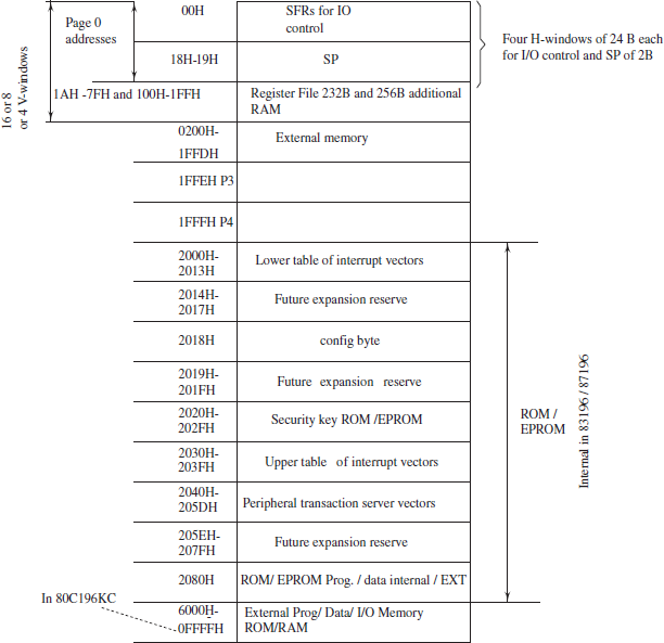
14.2 MEMORY MAP IN INTEL 80196 FAMILY MCU SYSTEM
Figure 14.3 shows the memory structure.
14.2.1 On-Chip RAM
An address, called direct address is used for accessing 8-bits. Page 0 is the address space between 0x0000 and 0x00FF. Page 0 addresses can be addressed by 8-bit direct address also. The 80196 SFRs are directly addressable as well as indirect addressable by programmer. Figure 14.4 shows the addresses at page 0 frame. Figure 14.5 shows complete memory map (addresses/address ranges) in 80196KC (16 kB on-chip ROM version) and 64 kB contiguous address space. When there are many SFRs and features, how to save them at page 0 frame itself. 80196 has solution in form of providing multiple windows for write and read.

Figure 14.3 Memory Structure
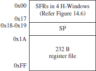
Figure 14.4 Page 0 frame in memory
Example 14.1
A byte at an address 0x25 can be accessed directly by using direct address 0x25 in the instruction. It is considered at page 0 frame.
Those addresses that are not needed for stack can be used as the assumed registers or memory. (A word is of 16-bit and a double word is of 32-bits. Stack is pointed by 16-bit SP. Stacking is of 16-bit words and therefore a stack must start from the even addresses.)
- A register or memory address is of 16-bits. Registers can be addressed by a direct address of 8-bit, indicating offset value on page 0 or a window.
- The 26 B SFR space has four H-windows. 24 Bytes at a window are for I/O control and 2 for SP.
- An H-window selects using WSR.
- Internal 512 RAM space (that includes SFRs) can be divided into 32 or 16 or 8 V-Windows using WSR. Using a V-Window enables use of direct address (offset value) within the window in an instruction.
Four H-windows in SFR Space
Four windows are horizontal window 0 (write), 0 (read), 1 (read/write) and 15. Horizontal windows 0-read and 0-write are identical in 80196 and 8096 MCUs. When reading from an address and when writing to an address, the different SFRs may be referred. This is like the existence of two windows, one when CPU reads and other when CPU writes. Window means at an address when using first window, CPU refer to one register and when using second window then refer to another register. The same address can be used for two purposes by the CPU. Windows in 80196 are used as follows:
(a) Internal SFRs Space in Memory
The lowest 24 B addresses in four windows (two in 8096) are SFRs addresses for the IO control. The two additional windows in 80196, horizontal windows 1 and 15 are for control and status bits of peripheral transaction server (PTS), additional PWMs, and additional ADC functions. Nine addresses between 0x00 and 0x19 are the same in all four windows. These nine are for the lower and upper bytes for zero register, two bytes for interrupt-mask registers, two bytes for interrupt-pending registers, one byte for window select register and two bytes for SPL-SPH.
Table 14.3 gives the meaning of symbols for the SFRs. The table also specifies full form and direct addresses of the 26 addresses of bytes at the SFRs (24 for IO control and 2 for SP). All addresses are 16-bit addresses in 80196. Table 14.3 also mentions the facts about the registers not present in 8096 version of 80196.
TABLE 14.3 Special Function Registers at Horizontal Window 0 (Read) and Window 0 (Write)
| Symbol | Full Form | Direct Address |
|---|---|---|
R0 |
Register 0-(Register 16 bits always 0s) |
0x00 and 0x01 |
AD_Command |
ADC command (when written) for the channel number and start |
0x02 |
AD_Result_LO |
ADC result lower byte (when read) |
0x02a |
HSI_Mode |
HSI mode command (when written) |
0x03 |
AD_Result_HO |
ADC result higher byte (when read) |
0x03a |
HSO_Time |
HSO unit time values for comparison at (registers of 16 bits each) (when written) |
0x04 and 0x05a |
HSI_Time |
HSI FIFO (first in first out) unit captured time values (when read) (at registers of 16 bits each) |
0x04 and 0x05a |
HSO_Command |
HSO unit Command values to CAMc (when written) |
0x06 |
HSO_Stat |
HSO unit status bits (when read) |
0x06a |
SBUF |
Serial receive buffer when read and transmit buffer when written |
0x07 |
INT_Mask |
Interrupt mask at PSW lower byted |
0x08 |
Interrupt pending register (same as 8096) to give which of the interrupt is pending |
0x09 |
|
Watchdog |
Watchdog Timer-16-bit Registere (when written) |
0x0A |
IOC2 |
IO control register 2 (when written) |
0x0B |
Timer 1 |
Timer 1-16-bit Registerf (when read) |
0x0A-0x0Ba |
Timer 2 |
Timer 2-16-bit Registerf (when read) |
0x0C-0x0D |
Baud_Rate |
Baud_Rate define 16-bit Registere (lower 14 bits baud rate and two msbs for clock source select (write Only) |
0x0E |
P0 |
Input Port P0 (read Only) |
0x0Ea |
P1 |
Port P1 (read and write) |
0x0F |
P2 |
Port P2 (read and write)g |
0x10 |
SP_Control |
Serial Port Control bits (write Only) |
0x11 |
SP_Stat |
Serial Port Status bits (read Only) |
0x11a |
INT_Pend1 |
Interrupt pending register 1 (not in 8096) to give which of the interrupt is pending |
0x12 |
INT_Mask1 |
Interrupt mask1 register (not in 8096) at PSW lower byted |
0x13 |
WSR |
Window Select register (not in 8096) b |
0x14 |
IOC0 |
HSO enable bits at four out-compare outputs (write only) |
0x15 |
IOS0 |
HSO status bits (read only) |
0x15a |
IOC1 |
IO control bits (write only) |
0x16 |
IOS1 |
IO status bits (read only) |
0x16a |
IOS2 |
IO Status register 2 (not in 8096) |
0x17 |
SP |
Stack Pointer 16-bitsh 0x18-0x19 |
|
a Same as above and appears distinctly at window 0 - read. Actually, there are two registers at the same address (es), one can be written and corresponds to window 0-write and the other can be read and corresponds to window 0-read.
b Writing b0 to b6 selects (changes) the window which is used later in the instruction. The b7 (msb) shows the hold pin status when read and is control bit for hold acknowledge when written. b6, b5 and b4 are written 0s when changing a horizontal window. The b3, b2, b1 and b0 then select the horizontal window. b3-b2-b1-b0 = 0000 means H-Window 0, 0001 means H-Window 1 (Table 14.4) and 1111 means H-Window 15 (Table 14.5)
c Content addressable memory.
d PSW lower bits are interrupt mask bits. PSW lower byte has an address assigned to it. PSW upper 8 bits are not addressable. However, PSW 16-bits can be pushed on stack and popped from RAM to find the upper 8-bits.
e Written with 8-bits twice by the byte transfer instruction for 0x0A.
f Read with 16-bits by word transfer instruction.
g Multiplexed with PWM(s), Sl-interface, INT and T2 control signals.
h Increments by 0x0001 and then push lower byte onto new pointed address (SP) and further increments SP by 0x0001 and then push higher byte. Pops the higher byte from new pointed address (SP), decrements the SP by 0x0001, further pops lower byte from new pointed address (SP) and decrements SP by 0x0001.
Figure 14.6 shows four H-windows in 80x96.
Example 14.2
Assume that a word at an address 0x0C-0D is accessed using 16-bit addressing instruction when-WSR register is set for window 0. The word will correspond to the 16-bit count in timer T2 of 80196 (Table 14.3).

Figure 14.6 Four Horizontal Windows in 80196 when WSR 3 Three Bits b6b50b4 = 000 (two in 8096); the Horizontal Windows is as per Bits at b3-b2-b1-b0
Table 14.4 gives the new SFRs that appear distinct at the read and write at window 1, which is called 1 because the last four bits in WSR (when selecting a horizontal window) are 0001.
TABLE 14.4 80196 New Special Function Registers at Horizontal Window 1 Read-cum-write
| Symbol | Full Form | Direct Addressa |
|---|---|---|
– |
Reserved for expansion |
0x02, 0x0A, 0x0B, 0x0D to 0x11, 0x15 |
AD_Time |
ADC time |
0x03 |
PTSSEL_LO |
Peripheral Transaction Server Service Channel Enable bits lower byte enable (Selects channel numbers enabled, which disabled) |
0x04 |
PTSSEL_HO |
Peripheral Transaction Server Service Channel Enable bits Higher byte (Selects channel numbers enabled, which disabled) |
0x05 |
PTSSRV_LO |
Peripheral Transaction Server End of Service Pending Flags lower byte |
0x06 |
PTSSRV_HO |
Peripheral Transaction Server End of Service Pending Flags higher byte |
0x07 |
IOC3 |
IO Control register 3 (T2 Internal Clock and PWMs) |
0x0C |
PWM2Control |
PWM 2 control register |
0x16 |
PWM1Control |
PWM 1 control register |
0x17 |
The remaining 9 addresses between 0x00 to 0x19H for the lower and upper bytes for zero register, two bytes for interrupt-mask registers, two bytes for interrupt-pending registers, one byte for window select register and two bytes for SPL-SPH are same as previous Window 0.
Example 14.3
Assume that a byte is written at an address 0x03. When WSR register is set for window 0, the byte will write at the HSI_Mode and will set the mode of HSI unit in 80196 (Table 14.3). When WSR register is set for window 1, the byte will write at the AD_Time and will set the time for ADC conversions at ADC unit in 80196 (Table 14.4).
Table 14.5 gives the new SFRs that appear distinct at the window 15 (called 15 because of the last four bits in WSR when selecting a horizontal window are 1111).
TABLE 14.5 New Special Function Registers at Horizontal Window 15
| Symbol | Full Form | Direct Addressa |
|---|---|---|
– |
Reserved for expansion |
0x0E to 0x10 |
– |
Not used |
0x02 to 0x07, 0x0A, 0x0B, 0x11H, 0x15H to 0x17H |
T2Capture_LO |
T2 Capture Lower Byte |
0x0C |
T2Capture_HO |
T2 Capture Higher Byte |
0x16 |
The remaining 9 addresses between 0x00 to 0x19H for the lower and upper bytes for zero register, two bytes for interrupt-mask registers, two bytes for interrupt-pending registers, one byte for window select register and two bytes for SPL-SPH are same as previous Window 1.
(b) Internal RAM/register File and Additional RAM Figure 14.1 showed that there is no accumulator. Figure 14.5 showed internal RAM/Register file at the third block from the top at page 0 addresses 1AH to FFH (232 B/116 words/58 double words) and additional RAM between 100H and 1FFH addresses. Pages 0 addresses can be addressed by an 8-bit direct address also.
V-windows in SFR and Internal RAM/register File Space
Concept of V-windows is similar to one of register banks in 8051. 8051 register bank consists of fixed number of banks = 4 and each bank has 8-registers. Banks are between addresses 0x00 to 0x1F.
V-windows in 80196 are between 0x0000 and 0x1FF, there are 512 bytes. Figure 14.7 shows the division of these addresses in sixteen or 8 or 4 vertical windows These can be divided into 32-bytes × 16 windows (Window 0, 1, 2,…. 15) or 64-bytes × 8 windows (Window 0, 1, 2,…. 7) or 128-bytes × 4 windows (Window read 0, write 0, read/write 1 and read/write 1…. 15). The write to b3-b2-b5-b4 bits of WSR register (Table 14.3) are used for switching between the horizontal windows (H-windows).
How can 512B address space be used and addressed by fewer bits than 9-bit address, which is otherwise required? 80196 has solution in terms of V-windows.
- The write to b6, b5 and b4 of WSR register (Table 14.3) are used for switching between the vertical windows (V-windows). b6-b5-b4 = 100, means division of512 bytes into 16 V-windows, which of the 16 windows, it is as per b3-b2-b1-b0 bits written/sent at WSR. b3-b2-b1-b0 = 0 means direct address referred is between 0x00 and 0x1F in each V-window. b3-b2-b1-b0 = 1111 means address between 0x01E0 and 0x01FF with direct address within the window between 0x00 and 0x1F. Figure 14.7(a) shows the 16 vertical windows.
- b6-b5-b4 =010 and b3 = 0 means into 8 V-Windows, which of the eight windows, it is as per b2-b1-b0 bits written/sent at WSR. b2-b1-b0 = 000 means direct address referred is between 0x00 and 0x3F. b2-b1-b0 = 111 means address between 0x01C0 and 0x01FF with direct address within the window between 0x00 and 0x3F. Figure 14.7(b) shows the eight vertical windows V0 to V!
- b6-b5-b4 =001 and b3-b2 = 00 means division of 512 bytes into four V-Windows, which of the four windows, it is as per b1-b0 bits written/sent at WSR b1-b0 = 00 means direct address referred is between 0x0000H and 0x007F. b1-b0 = 11 means address between 0x0180 and 0x01FF with direct address within the window between 0x00 and 0x7F. Figure 14.7(c) shows the four vertical windows V0 – V3.
- b6-b5-b4 = 000 means select a horizontal window as per b3-b2-b1-b0. Direct address bytes can then be between 0x00 and 0xFF.
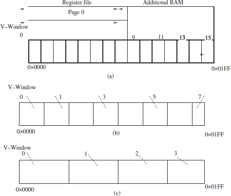
Figure 14.7 Vertical Division of Address Space Between 0x000 and 0x1FF in the Memory map: (a) Sixteen V Windows Each of 32B, (b) Eight V Windows, Each of 64B and (c) Four V Windows, Each of 128B
Example 14.4
Assume that WSR register bits b6-b5-b4 =001 and b3-b2 = 00. It means vertical division of 512 bytes into 4 V-Windows. Four V-windows are between 0x00 to 0x7F, 0x80 to 0xFF, 0x100 to 0x17F and 0x180 to 0x1FF [Fig. 14.7(c)].
When b1-b0 = 10, it means V-window is between 0x100 and 0x17F. A register file register at address 0x124 can be assessed by offset address 0x24 using direct address instruction.
14.2.2 On-Chip ROM/EPROM
(a) Interrupt and PTS Vectors Figure 14.5 showed that seventh and twelfth blocks are for two sets of the addresses (lower table and upper table). These are for the interrupt vectors. PTS vectors are 2040H to 205DH. These point to the addresses for DMA service and peripheral routines. The routines are associated with the peripherals. A peripheral does the IO transactions with the system.
(b) Configuration and Security-key Figure 14.5 showed that at 2018H there is a configuration register of 1 byte. It is for enabling or disabling power-down feature, bus-width select 16 or 8, write mode select (whether ![]() and
and ![]() signals or
signals or ![]() and
and ![]() signals), using ALE or
signals), using ALE or ![]() , control bits for internal ready control mode and program lock mode.
, control bits for internal ready control mode and program lock mode. ![]() means byte high enable when active. This means odd address enable when writing a byte to memory. ALE means address latch enable when signal = 1 like in 8051 and
means byte high enable when active. This means odd address enable when writing a byte to memory. ALE means address latch enable when signal = 1 like in 8051 and ![]() means address valid and latching of address when 0. Security key has 128 bits between 2020H and 202FH.
means address valid and latching of address when 0. Security key has 128 bits between 2020H and 202FH.
(c) Internal Program-cum-data ROM/EPROM The program starts from 2080H on reset. Internal program as well as data stores at ROM in 83196 and at EPROM in 87196 up to the address 0x5FFF. These address are accessed from the off-chip memory if EA is 0. During development phase before the codes are burned, an external PROM can be used.
14.2.3 External Program/Data Memory (PROM/RAM) Space
Figure 14.5 showed in lowest block address for the external PROM /RAM/IO of peripherals. These are between 0x6000 and 0xFFFF in 80196KC family.
14.3 IO PORTS
80196 has the following IO features:
- Use of PTS facilitates DMA. PTS is a special feature in the select version of 80196 family.
- There are five ports in single chip mode. Port P0 is input port only and also functions for the multi-channel analog inputs. Ports P1 and P2 are used for PTS IO signals, PWM outputs, serial IO and T2 clock and reset signals in expanded chip mode.
Large number of IO peripherals (ports) can be interfaced in the expanded mode. This is because there is memory mapped IOs (IOs peripherals accessed like a memory address).
A large program memory can be interfaced. An instruction fetch valid signal, INST helps in finding when there are codes at the bus from external program memory codes. Ports P0 to P4 uses are as follows:
Input Port P0 P0 (address 0x0EH in Window-0 read) has 4 bits (P0.4 to P0.7) in 48-pin version and 8 bits (P0.0 to P0.7) in 52-pin version. There can be analog inputs when using AD. Separate pins are used for V+ref and analog ground. When ADC is not used, P0 pins accept digital input bits also. When using an external device P0.7 is used for external interrupt, EXINT1.
IO Port P1 P1 (address 0x0FH in Window-0 read, Window-0 write) has eight IO bits, P1.0 to P1.7. P1 is quasi bi-directional port. It means for a short period it can interface a 74LS TTL latch else it is open drain port. Port pins P1.7–P1.6 and P1.5 are used for PTS HOLD/HLDA signals. When using three PWMs, the Port pins P1.4–P1.3 are used for PWM 1 and PWM 2 output bits.
IO Port P2-cum-devices Port P2 (address 0x10 in Window-0 read, Window-0 write) has eight IO bits, P2.0 to P2.7 and is bi-directional. Any unused port pin P2.x has the same loading and driving capability as P1.x. When using the PWM0, P2.5 is PWM output. When using timer T2, P2.4 and P2.3 pins are used as inputs T2CLK (timer 2 clock) and T2RST (timer 2 reset) for the timer. When using an external device P2.2 is used for external interrupt, EXINT.
Serial Port When using serial interface (SI) similar to 8051 SI, the P2.0 and P2.1 are interfaced to carry the data and clock or TxD and RxD during the serial synchronous communication or UART communication, respectively.
Ports P3 and P4 P3 and P4 (addresses 0x1FFE and 0x1FFFH) has eight IO bits, P3.0 to P3.7 and P4.0–P4.7 are quasi bi-directional that means for a short period, it can interface 74LS TTL latch else it is an open drain port. These carry address and data bits (Fig. 14.2).
14.4 TIMERS
80196 MCU has two timers—timer 2 and timer 1. Both Timer T1 [16-bit free- running counter (FRC)] and T2 [16-bit event counter] can be used for the high-speed outputs (HSO) and high-speed input (HSI) captures.
(a) Timer T1 Assume using a 16 MHz crystal. The counter inputs are internal and are at the periodic intervals of 1.66 μs (Section 6.1). Timer 1 functions as a 16-bit free- running counter (FRC) (Section 6.2). Word address for the SFR for T1 is 0x0A-0x0B window 0(read). H-Window for the SFR for count word for T1 is window 0(read). After a read from window0-read, T1 word can be used to save. The save can be after the increment or decrement or complement or shift operations, or arithmetic or logic operation. T1 is used for the real-time control. T1 features are similar to ones described in Section 6.2.
Example 14.5
SFR for T1 word at an instance is read and is equal to 0x7FFF. Assume that it is read again after 10 periodic intervals of 1.66 μs. What will be the value in T1?
0x7FFF + 0x000A = 0x8009.
(b) Timer T2 T2 is 16-bit event counter. T2 can be reset internally or externally. T2 can be reset internally or by an external input or by an out-comparison using T1. T2 can be clocked externally in 80196KB and internally also in 80196KC. When T2 is used as counter, it counts the transitions at the input T2CLK (at P2.4). The minimum time between two successive edges (+ve followed by −ve or −ve followed by +ve) can be 1.66 μs for 16-MHz crystal.
T2 can be reset by input at P2.3 pin T2RST (timer 2 reset). Timer T2 can also be reset by an HSI input capture. The count can be read at Timer 2 SFR. T2 SFR word address and window are 16-bit word 0x0C-0x0D and window 0 (read).
Example 14.6
T2 is reset by input at T2RST pin. If T2 SFR is read at that instance, what will be value? If it is read after 20 input edges at T2CLK pin, then what will be the value?
Just after reset, the counts will be 0x0000 at T2 SFR at window 0 0x0C-0x0D. After 20 (= 0x14) input edges, the T2 counts = 0x0000 + 0x0014 = 0x0014.
Refer Table 14.3. The control and status registers for timer 2 and timer 1 are IOC0, IOC1, IOS1 and IOS2. The table save the addresses and windows. IOS1 has the T1OV and T2OV overflow flags. The flags are used to indicate timeouts of timers 1 and 2. IOC1 has the T1OVIE and T2OVIE. These are interrupt on overflow enable bits. These unmask the interrupts on timeouts of timers 1 and 2. IOC0 has control bit which enables the HSI captures of time. The captured time saves into a FIFO. There is a control bit to enable clear of T2 when there is external input at T2RST (Port P2.3 pin). The control bit can be used reset T2 internally also.
- T1 and T2 can be used for comparing the preset instances with timer values and generation HSO outputs or software timer interrupts or A/D start. These instances for comparison are written into an HSO_CAM. Each CAM entry can be in any order. It has 16 bits for a timing instance to be compared with either T1 or T2 and 7 bits for command and action control.
- There are three PWM outputs PWM0, PWM1 and PWM2.
- There is watchdog timer.
14.5 HIGH-SPEED OUTPUTS
HSOs, and HSO CAM are special features in 80196 family MCU.
Consider Example 14.7 to explain why we need a high-speed timer-output comparison unit.
Example 14.7
Assume that a free- running counter T1 is running and incrementing after every 1.66 μs. We wish to initiate the actions when its contents are 0x1000, 0x2000, 0x4000 and 0x8000 so that actions takes place at time values = 4096 × 1.66 μs, 8192 × 1.66 μs, 16384 × 1.66 μs and 32768 × 1.66 μs. One method can be to read the T1 SFR values continuously.
- when (T1 = = 4096) Action 1 by running ISR1
- when (T1 = = 8192) Action 2 by running ISR2
- when (T = = 16384) Action 3 by running ISR3
- when (T = = 32768) Action 4 by running ISR2
However, suppose AD conversion is over and the MCU is executing ISR_AD after end of conversion and at that instance the T1 counts become equal to 16384. Action 3 will be delayed till there is return for the ISR_AD.
MCU 80196 high-speed output (HSOs) functions give an elegant way of solving the problem of actions with least delays.
An additional feature in 80196 is that there are high-speed output (HSOs) functions. The highspeed outputs (to external pins) are generated by high-speed comparison (with a resolution of 1.66 ^s for a pin) by comparing the timer T1 or T2 values using the preset values in CAM (content addressable memory). A CAM (content addressable memory) holds entries. A CAM entry can be written in any order unlike the entries pushed into a stack or entries inserted into a queue. CAM can be understood by Example 14.8.
Example 14.8
Assume that an account number AC1= 10235 is having amount AMT1 = 20000, AC2 = 10236 is having amount AMT2 = 20500, AC3= 10237 is having amount AMT3 = 10000, AC4= 10239 is having amount AMT1 = 40500.
When we write in content addressable memory (CAM), we can write first entry = 10237, 10000, second entry = 10239, 40500, third entry as 10235, 20000 and fourth entry as 10236, 20500.
We can alternatively enter AC4 entry first and AC1 next or any way we like. Irrespective of the order in which entries are made the contents are equivalent. The AMT3 value is found by using AC3 from the CAM, the AMT2 value is found by using AC2. The key and its value define each entry. Hardware on sending the key, if the key matches with set of keys saved at CAM, then generate the value corresponding to the key.
14.5.1 HSOs
A high-speed output means the activation of a pin called HSO.x pin. x can be 0, or 1 or 2 or 3 or or 5. Any of six HSO.x pin can be program to obtain any of the six independent programmable (‘1’ or ‘0’) output. HSO.0 and HSO.1 pins can be jointly used to get outputs. HSO.2 and HSO.3 pins can be jointly used to get outputs. 8 type of HSO output at the pins are are programmable by command bits in HSO_CAM as described below. The CAM entries are as per Table 14.6. A program instruction makes a CAM entry by first writing 24 bits to HSO_COMMAND register at 0x0006 (write).
An HSO output generates, when comparison of the 16-bit time value entered in an HSO entry is successful with respect to the count C(T1) at T1 (frre-running counter) or count C(T2) at T2 (event counter) value at an instance.
A CAM entry is as shown in Table 14.6. CAM entries are made using 23-bit HSO Holding register. The register has two parts HSO_Timer and HSO_Command. At each entry, there is a timer identity, timer instance is programmed set for comparison. The command-bits are programmed for HSO output at a specific pin or any other action to be taken. HSO_CAM can have a maximum of eight entries, each of 23 bits. The 23 bits in one single entry in HSO_CAM have lower 16 bits that are used for comparison with timer 1 or timer 2 value on SFR read. Upper b16-b22 bits of an entry are the channel bits, timer identity bit and command bits as shown in Table 14.6.
TABLE 14.6 A CAM Entry in HSO CAM (Maximum Number of Entries can be 8 and can be made in any Order)
| Bits | Meaning | Action |
|---|---|---|
Time value (b15-b0) |
16-bit to define the value, c which needs to be compared with counts C(T1) or C(T2) continuously |
When T1 or T2 counts C(T1) or C(T2) becomes equal to the b15-b0 16 bits in the entry, then take action at the channel defined by HSO_Command bits b3-b2-b1-b0 |
HSO_Command bits b2-b1-b0.a [ means b18-b17-b16] and b3=0 [b19] |
Defines channel for action: 0000 means HSO.0 pin, 0001 means HSO.1 pin, and so on; 0101 means HSO.5 pin; 0110 means pair of pins HSO.0 and HSO.1; 0111 means pair of pins HSO.2 and HSO.3 |
Programmable output takes place at pin HSO.0 or HSO.1 or …. or HSO.5 or at pair HSO.1 and HSO.0 or pair HSO.2 and HSO.3 as per defined channel 0, 1, 2, 3, 4, 5, 6 or 7 for the action |
HSO_Command bits b3-b2-b1-b0 [ means b19-b18-b17-b16] |
1110 reset T2 |
Timer T2 resets to 0 when b15-b0 value = 0 counts |
HSO_Command bit b4 [b20] |
When = 1 for generating interrupt |
Generate HSO interrupt also |
Command bit b5 [b21] |
When = 1 HSO.x pin = 1 when = 0 HSO.x pin = 0 |
Programs the output pin after the b15-b0 value = on counts |
Command bit b6 [b22] |
When = 1 Use timer 2 when = 0 Use timer 1 |
Programs to use which of the timer T1 or T2 for comparison |
Command bit b7 [b23] |
Not used |
not used |
a When x is between 000 and 101 where x=b2 -b1-b0, it means generate the output at pin HSO.x on a successful comparison.
The control and status bits are set or reset. Table 14.7 lists the meanings and actions.
TABLE 14.7 Control Bits at IOC1 (IO Control Register 1 at 0x0016 (Write) and Status Bits at IOS0 at 0x0015(Read)
| Bits | Meaning | Action |
|---|---|---|
IOC1.6 |
IO control 1 register bit 6 |
1. Enable HSO.5 for the HSO output when set = 1 |
IOC1.4 |
IO control 1 register bit 4 |
1. Enable HSO.4 for the HSO output when IOC1.4 = 1 |
IOS0.0 to IOS0.5 |
IOS0 register bits 0 to 5 |
Status of HSO.0, …., HSO.5 |
IOS0.6 |
IOS0 bit 6 |
HSO holding register full or CAM full |
IOS0.7 |
IOS0 bit 7 |
HSO holding register full |
All the high-speed outputs or A/D or start of software-timer related ISR execution or A/D conversion start can take place independently at high speeds but resolution will be 1.66 μs for 16 MHz XTAL.
14.5.2 Software Timers
Software timer interrupt does not generate a pin output on successful match of C with C(T1) or C(T2). The match is after comparison is between C(T1) or C(T2) with the preset time value C in the CAM for the corressponding command bits in that entry. It generates software timer interrupt when status flag IOC1.y = 1, where y − 0 or 1 or 2 or 3. When the channel bits b3-b2-b1-b1 in the command register are set or reset such that they are in between 1000 and 1011, then set the corresponding status flag and start a software timer 0 or 1 or 2 or 3 interrupt (if enabled) service routine when comparison shows the match of c and C.
Four software timers are programmable by command bits in HSO_CAM as described below. The CAM entries are as per Table 14.8. Instruction is used to we make a CAM entry by first writing to HSO_COMMAND register at 0x0006 (write). Then we write to HSO_Time at 0x0004-0x0005 (lower and upper bytes). Bits b20 to b23 are as per Table 14.7. Bits b0 to b15 are as per HSO_Time bits.
TABLE 14.8 A CAM Entry in HSO CAM (Maximum Number of Entries can be 8 and can be Made in any Order) for use of SWTs
| Bits | Meaning | Action |
|---|---|---|
HSO_Command bits b3-b2-b1-b0. [b19-b18-b17-b16] |
Defines channel for action: 1000 |
Programmable SWT0, SWT1, SWT2 or SWT3. as per defined channel 8, 9, A or B for the action. Set status flag and start |
Flags for interrupts of software timer 0, software timer 1, software timer 2, and software timer 3, are the bits at IOS1.0, IOS1.1, ISO.2 and ISO.3, respectively (Table 14.9). The interrupt occurs if primary level I bit of PSW is also set. Software timers are alternatives to real time interrupts in 68HC11.
All the high-speed outputs or A/D or start of software-timer related execution of an interrupt service routine or A/D conversion start can start independently at high speeds but resolution will be 1.66 μs for16 MHz XTAL.
The status bits are set or reset as given in Table 14.9.
TABLE 14.9 Control Bits at IOC1 (IO Control Register 1 at 0x0016 (Write) and Status Bits at IOS1 at 0x0016(Read)
| Bits | Meaning | Action |
|---|---|---|
IOS1.0 to IOS0.3 |
IOS1 register bits 0 to 3 |
Status of Software timer 0, 1, 2 and 3 |
14.5.3 Start of ADC Using T1 or T2
Channel bits in the command register HSO_Command are 1111, the A/D conversion starts when comparison with HSO_Time bits (means time value c) shows that C(T1) or C(T2) becomes equal to c.
ADC start time is programmable by command bits in HSO_CAM as described below. The CAM entries are as per Table 14.10. Bits b20 to b22 are written in the entries as per Table 14.7. A CAM entry is written by instruction by first writing to HSO_COMMAND register at 0x0006 (write) and then write using instruction to HSO_Time at 0x0004-0x0005 (lower and upper bytes).
TABLE 14.10 A CAM Entry in HSO CAM (Maximum Number of Entries can be 8 and can be Made in any Order) for ADC and HSO_Time
| Bits | Meaning | Action |
|---|---|---|
Time value c in b15-b0 in HSO_Time |
16-bit to define the time value, which needs to be compared with counts C(T1) or C(T2) continuously |
When T1 or T2 counts C(T1) or C(T2) becomes equal to the c in the entry, then take action at the channel defined by HSO_Command bits b3-b2-b1-b0 |
HSO_Command bits b3-b2-b1-b0. [b19-b18-b17-b16] |
Defines channel for action: 1111b ADC start |
Programmable Start of AD conversion when defined channel = 0xF for the action |
14.6 HIGH-SPEED INPUTS AND INPUT CAPTURES
HSI and use of HSI FIFO are special features in 80196 family MCUs. When an event occurs, a signal may be generated (1 or 0). It is required to find the instance of time at which the input signal occurred. As soon as the signal occurs, the timing instance at T1 needs to be captured in some register. T1 can be used for capturing instances of inputs occurring at high speed. There is FIFO of total eight maximum possible entries and each entry of 20 bits, 16 for timing instance and four to identify the input source. On the occurrences at the high-speed inputs (at specific external pins), Timer 1 values at those instances are captured. High speed means capture is instaneous and next instance can be captured with the internal clock resolution, 1.66 μs and put in the HSI_holding register. Assume that the next capture occurs fast, before the action is taken on that. The captured entries save at a FIFO, which can have a maximum of eight entries. Presence of FIFO enables the fast capture of next instance.
HSI capture can be on accurance of any of the four independent programmable edge transitions at the 4 input pins, HSI.0 to HSI.3.
Table 14.11 shows the HSI_mode bits for programming of HSI.z pins (z = 0, 1, 2 or 3).
TABLE 14.11 HSI_Mode Bits for the Programming HSI Input Instances for the Capture of Time from T1
| Bits | Meaning | Action |
|---|---|---|
HSI Mode bits b7-b6, b5-b4, b3-b2 and b1-b0 at 0x0006 (write) for HSI.3, HSI.2, HSI.1 and HSI.0, respectively |
Pair of bits each for HSI.3, HSI.2, HSI.1 and HSI.0 modes |
b7-b6 = 00 means every eight +ve edge sensed at HSI.3. When 01, sense every +ve edge, when 10 sense every −ve edge and when 11 sense +ve as well as −ve edge at HSI.3. Similarly the modes of HSI.2, HSI.1and HSI.0 by 3 pair of bits. |
The control bits are given in Table 14.12.
TABLE 14.12 IOC0 Control Bits for the HSI.z Captures
| Bits | Meaning | Action |
|---|---|---|
IOC0 control bits b6-b4-b2-b0 at 0x0015 (write) |
Defines input for action: 0001 means HSI.0 pin, 0010 means HSI.1 pin, 0100 means HSI.2 pin, 1000 means HSI.3 pin |
Programmable input takes place at pin HSI.0 or HSI.1 or HSI.2 or HSI.3 as per defined pin for input. b6-b4-b2-b0 = 1111 means enable all 4 inputs at HSI, 0000 means none. |
Capture values (HSI_Time) of C(T1) along with the identity of input (HSI status) that is captured, is saved in a holding register then to a FIFO. The register or FIFO can be read later. The read must be before the next capture after the instance of FIFO full interrupt. This ensures that no time is taken in first saving the captured result then readying for the next capture that is the case when FIFO is not provided in the MCU like 68HC11.
HSI_Time is a SFR word and when read gives the input capture time value. A maximum of seven entries can wait after the first capture in the FIFO before it becomes compulsory to read captured values from FIFO (otherwise the next captured time cannot be saved). FIFO has 20 bits for each entry. The 16 entries are the HSI_Time indicating a timer 1 instantaneous value C(T1) when the capture occurred. Four bits b7-b5-b3-b1 at HSI_Stat SFR indicate which HSI.z caused the capture at the FIFO (z = 3, 2 or 1 or 0). Table 14.12 shows the HSI_Time, HSI_Status and IOS1 status bits for the FIFO status.
Table 14.13 shows the HSI_Status and IOS1 status bits for the FIFO status.
TABLE 14.13 HSI_Time Captured on Input, HSI_Status and IOS1 Status Bits for the FIFO Status
14.7 PULSE WIDTH MODULATED OUTPUT
A SFR is for PWM_CONTROL. It controls the PWM output. PWM output enables at P2.5 when a control bit at IOC1.0 SFR is programmed as 1. There is an internal 8-bit free- running counter that is internally clocked every 0.1875 (=3/16) μs clock inputs (for 16 MHz XTAL).
Table 14.14 shows the PWM_Counter bits which are used for using PWM.
TABLE 14.14 PWM_Counter (No Address Exists to Read or Write it)
| Bits | Meaning | Action |
|---|---|---|
PWM_Counter b7-b6-b5-b4-b3-b2-b1-b0 |
Count the clock inputs every 0.1875 (=3/16) us for 16 MHz XTAL |
Time out every 48 μs |
The control bits are given in Table 14.15.
TABLE 14.15 IOC1 Control Bits and PWM _Control Bits for the PWM Output
| Bits | Meaning | Action |
|---|---|---|
PWM_Control 1 b7-b6-b5-b4-b3-b2-b1-b0at 0x0017 (write) |
Count the clock inputs every 0.1875 (=3/16) μs for 16 MHz XTAL |
Output = 1 (if enabled) at P2.5 when PWM_Counter = 0 and output=0 when PWM_ Control 1 = PWM_Counter counts |
PWM_Control 2 b7-b6-b5-b4-b3-b2-b1-b0at 0x0016 (write) in 80196KC |
Count the clock inputs every 0.1875 (=3/16) μs for 16 MHz XTAL |
Output = 1 (if enabled) when PWM_Counter = 0 and output=0 when PWM_Control 2= PWM_Counter counts |
IOC1 control bit b0 at 0x0016 (write) |
b0 = 1 enable PWM output at pin P2.5 |
Enable or disable PWM output |
When using PWMs, the Port pins P1.4–P1.3 are used for PWM 1 and PWM 2 output bits.
Additional PWM Output
HSO outputs can be used for additional PWM outputs. On the overflow, we can set the HSO.x pin and enter a new entry in the CAM with HSO_Time. When the comparison is successful we can reset the HSO.x pin.
Additional PWM Output at Pair of Pins HSO.0-HSO.1 or HSO.2-HSO.3
On the overflow, we can set = 1 two HSO.x pin pairs 0 and 1 or 2 and 3. Enter a new entry in the CAM with HSO_Time2 and HSO_Time 3. When the comparisons are successful, we can set the HSO.x pin 0 or 1 or 2 or 3 = 0.
Let use the CAM entries in the following method. At the overflow of T2, the HSO_Time is set at 0x0080 for HSO.2 output and at 0x0100 for HSO.3 output. Then the HSO.2 and HSO.3 outputs are made = 1. Now when C(T2) becomes 0x0080 and then the HSO.2 output (PWM output 1) is made = 0 and when C(T2) = 0x0100 the HSO.3 is made 0. Now, T2 is reset at C(T2) = 0x0200 and the HSO.3 and HSO.2 are both set to 1.
- We get 1 for duration of T2 counts between 0x0000 and 0x080 at HSO.2 and 0 for duration of T2 counts between 0x080 to 0x0200. The duty cycle = 25% at HSO.2. HSO 2 output is PWM output 2.
- We get 1 for duration of T2 counts between 0x0000 and 0x100 at HSO.2 and 0 for duration of T2 counts between 0x0100 to 0x0200. The duty cycle = 50% at HSO.3. HSO 3 output is PWM output 3.
14.8 INTERRUPTS
14.8.1 Non-maskable and Maskable Sources of Interrupts
NMI pin, unimplemented opcode, and trap instruction interrupts are the non-maskable sources of interrupts. All interrupt sources can be grouped according to their group priority when servicing them using ISRs. There is an ISR and an interrupt vector for each group. Processor vectors to the interrupt vector address to execute the ISR. The ISR executes in case the interrupt is non-maskable interrupt or is or un-masked by writing into INT_Mask and INT_Mask 1. Masking is done by bits at the INT_Mask (in 80196 and 8096) and INT_Mask 1 (not in 8096). Primary-level mask is I bit at PSW.9 in the PSW. Table 14.6 gives the groups and sources and flags in each group.
TABLE 14.16 Priority-wise Groups and their Sources and Flags in Each Group
| Group | Meaning | Interrupt Instance |
|---|---|---|
NMI Group 0 |
Interrupt at NMI Pin (Highest Priority) |
|
INT_Mask1 Group 1 |
Interrupt at HSI unit |
FIFO full |
INT_Mask1 Group 2 |
EXINT1 P0.7 pin Interrupt |
EXINT1 |
INT_Mask1 Group 3 |
T2 Overflow |
Flag T2OVF |
INT_Mask1 Group 4 |
T2 Capture when internal clocking |
T2CAP |
INT_Mask1 Group 5 |
HSI FIFO half-full interrupt |
FIFO 4th Entry |
INT_Mask1 Group 6 |
Serial Receiver RI set |
Flag RI |
INT_Mask1 Group 7 |
Serial Transmitter Empty TI set |
Flag TI |
Group 8 |
Unimplemented opcodea |
Watchdog timer timeout |
Group 9 |
Instruction Trapb |
– |
INT_Mask Group 10 |
External Interrupts, EXINT |
Port P2.2 pin for interrupt |
INT_Mask Group 11 |
SI interface Interrupts. Any or both TI (transmitter interrupt) and RI (receiver Interrupt) |
TI and RI flags |
Software Timers Interrupts, ADC start, and T2 reset |
Status of Software Timers 0, 1, 2 and 3, ADC and T2 reset started by the HSO unit comparisons of preset instances with T1 or T2 |
|
INT_Mask Group 13 |
HSI pin 0 input instance Interrupt |
Status of HSI.0 pin |
INT_Mask Group 14 |
HSO Interrupts HSO.0 to HSO.5 |
Status of HSO output pins |
INT_Mask Group 15 |
Interrupts from the HSI capture data ready and FIFO full |
Flags for HSI captured an input, FIFO fourth entry received and HSI FIFO full |
INT_Mask Group 16 |
A/D conversion over interrupts |
Status ADC over |
INT_Mask Group 17 |
Interrupts from Any or both T1 and T2 (lowest priority) |
Flags for T1 (IOS1.5) and T2 overflows |
a When there is watchdog timer timeout there are unimplemented instructions. Unimplemented means yet to be executed.
b It is an instruction; it enables interrupt vectoring for an ISR. The ISR is then usually used to debug or pause a program for finding status of variables, registers and ports.
14.8.2 Servicing of Interrupts
Sixteen bits, at interrupt pending registers, INT_Pend and INT_Pend 1 indicate the pending sources. INT_Mask and INT_Mask 1 registers indicate the un-masked sources. PSW. 9 indicates whether all maskable sources masked. Service initiates by vectoring to the vector address for that group according to the group priority (group 0 highest, 17 lowest (Table 14.6); Group 17 down to 0 interrupts have vector addresses in 80196 from 0x2000−0x2001 to 0x203E−0x203F).
14.9 INSTRUCTIONS AND INSTRUCTION SET
Initial Conditions
When there is power up reset or other reset for example when RST instruction executes, IOs Control SFRs, PC, flags in PSW acquire the same value as acquired on CPU power up, and all six flags Z, N, V, C, VT and ST get reset. (ii) a pulse is sent at reset pin to enable reset of other interfaced programmable peripherals.
Addressing Modes
Register/memory addresses are contiguous in 80196 and there are no registers (other than the SFRs) that are dedicated specifically for arithmetic and logic operations and indirect address pointers. Therefore, conventionally it is assumed that there are registers at the register file. Registers chosen in analogy to the 8086 are AL, AH, BL, BH, CL, CH, DL, DH, SI (LO), SI (HO), DI (LO), and DI (HO) to memory page 0 addresses from 001CH to 0024H, respectively. SI (LO) and SI (HO) are lower and higher bytes of 16-bit SI (Source Index) register. DI (LO) and DI (HO) are lower and higher bytes of 16-bit DI (Destination Index) register. One of the four addressing modes can be used in an instruction set.
- Implicit, Examples are as follows (i) SETC, set C in PSW. (ii) POPF and PUSHF pop and push PSW, respectively. (Pop instruction transfers PSW from stack to destined operand and decrements SP by 2.)
- Direct (also called register direct or page 0 address direct).
Three-byte instruction, LD BD, BS to load a byte from direct address (or register) to another destination address (register) BD. Another example is ADD WD, WS1, WS2 to add word from direct addresses (of 8-bit each from WS1 and WS2 and places the result at the direct address WD. WD can be AX or BX or CX.
3. Immediate
Example 14.11
Three-byte instruction, LD WD, #3000H to load a word 0x3000 at a word destination address WD. Another example is ADD WD, WS1, #data16 that adds the word from direct address WS1 with immediate-word data16 in the instruction as immediate operand and places the result at direct address WD. ADD WD, #data16 is another example in source-cum destination operand is WD and data16 is added and result saved there. WS and WD can be assumed AX or BX or CX.
4. (i) Indirect without auto post increment of the pointer, (ii) indirect with auto post increment of pointer, (iii) indexed short (displacement is 1 byte two’s complement number defined within the instruction to the pointed address by the index defined within the instruction) and (iv) indexed long (offset of 2 bytes unsigned number defined within the instruction from a pointed address by the index defined within the instruction).
Example 14.12
(a) ADD WD, WS1, [WS2] adds 16-bits word at operand from direct address WS1 with a address pointed by WS2, (b) ADD WD, WS1, [WS2]+ adds operand from direct address WS1 with address pointed by WS2 and then increment the WS pointer (by 2 because it is a word pointer), (c) ADD WD, WS1, WS2 [offset] operand from direct address WS1 with a direct address pointed by WS2 after adding it by offset (WS2 does not change) and (d) ADD WD, WS1, disp [WS2] to add operand from direct address WS1 with address pointed by WS2 after adding it by two’s complement 8-bit displacement (WS2 does not change and the pointed displacement is negative or positive between –128 and 127). [WS2] can be an assumed to be a SI (source index register).
Data Transfer Instructions Instruction set has the following data transfer instructions for load: LD, LDB, LDBZE, LDBSE, for load word, byte, word with byte and integer with short integer, respectively. ST and STB are for store into memory from register a word or byte, respectively. BMOVE instruction for block move is available at 80196KB.
A byte transfers to a byte address or a word address in a data transfer instruction or a word transfers to a word address in a data transfer instruction.
Example 14.13
ST XD, YS instruction. It stores from a direct page 0 address source-operand YS to destination-operant XD. The source operand may be addressed by any of the six ways, direct, immediate, indirect, indirect with pointer auto increment, or indirect short or indirect long. Similarly, there are the instructions, LD (load), PUSH and POP instruction each with six ways for specifying a source operand.
Stack (Push and Pop) Instructions Instruction set has the following stack (push and pop) instructions for Push: PUSH, PUSHF and PUSHA for pushing the word, flags and all (in 80196KB) and for Pop: POP, POPF and POPA for pushing a word, flags and all (in 80196KB).
Data and Bit—Manipulation Instructions Instruction set has the following data transfer initialization (manipulation) instructions: SETC to set carry, CLRVT to set overflow trap, CLRC to clear carry, CLRB and CLR to clear at byte and word, respectively.
Example 14.14
- At a destined operand, a byte or word or long word (32 bits) can be made 0s by CLRB XD or CLRW XD or CLRLD XD instruction.
- At a destined operand, a byte or word can be extended to a word or a long word by sign bit extension by EXTB XD or EXTW XD instruction. Similarly, normalization of (i) a byte into a word or long word or (ii) a word into a long word can also be done. Normalization is simply putting 0s at the higher bytes.
- At a destined operand, a byte or word or long word (32 bits) can be complemented by NOTB XD or NOTW XD or NOTLD XD instruction. At a source an operand byte or a word or long word (32 bits) can be made to either arithmetic shift-left or shift-right or logical shift left or right. Number of times the shifts is needed, can be specified at the instruction.
- Certain instructions affect a specific bit. For example, EI and DI affect the PSW.9 (I bit) to enable or disable interrupts of maskable sources at primary level. CLRC and SETC make C = 1 and 0, respectively. CLRVT makes VT = 0.
Instructions for Arithmetic or Logical Operations Arithmetic and logical instructions operate on the word operands or byte operands at the direct address (destination address or source cum destination address is a direct page 0 address after the opcode). The instructions are three to seven bytes long. Second source can be the direct or indirect addressing ways described above.
Instructions for arithmetic operations are the following:
- (i) ADD for add words, (ii) ADDB for add bytes, (iii) add with carry and word and (iv) ADDCB add with byte and carry.
- SUB for subtract of word, SUBB for subtract byte, SUBC subtract word and borrow, and SUBCB for subtract byte and borrow (C’s complement).
- MUL, MULB, MULU and MULUB for (i) multiply with word (ii) multiply with byte (signed numbers) and (iii) multiply with word (unsigned numbers) and (iv) multiply with byte (unsigned numbers), respectively.
- DIV, DIVB, DIVU and DIVUB for (i) dividing word (ii) divide byte (signed numbers) (iii) divide unsigned numbers and (iv) divide byte (unsigned numbers), respectively.
- INC and INCB for incrementing word and byte, and DEC and DECB for decrementing word and byte [two byte instructions are for increment and decrement at a source-cum-destination direct address.].
- NEG and NEGB for two’s complementing word and byte [instructions are for negation (two’s complementation) at a source-cum-destination direct address].
- EXT and EXTB for sign extension of integer to long integer and short integer to integer.
- NORML for normalizing the long-integer.
Instructions for logic operations are as follows:
- AND, OR and XOR instructions are for logical operations on words and ANDB, ORB, and XORB instructions are for logical operations on bytes
- CMP, CMPB and CMPL for comparison (by hypothetical subtraction) of word, bytes and long-words (in 80196KB).
Flag changes are as follows—C = 1 if there is a carry on add or increment or a no borrow on subtraction or decrement or negation, else will be 0. Z = 1 if in all bits there are zeros on increment or decrement or negation, else it will be 0. V = 1 if there is an overflow during two’s complement operation, else will be 0. N (negative flag) = 1 on result maximum significant b15 or b7 = ‘1’, for word or byte operations, respectively, as set 1, else will be 0. VT flag may be 1 on overflow if 0 earlier but not vice versa as VT can only be reset to 0 by CLRVT instruction.
Instructions for Shift Operations
Instructions for shift operations are as follows:
- SHL, SHLB and SHLL for shift left of word, bytes and double-words (in 80196KB).
- SHR, SHRA, SHRB and SHRAB for shift logical right of word, shift arithmetic right of word shift logical right of byte, shift arithmetic right of byte, respectively. SHRL and SHRAL for shift logical right of double word and shift arithmetic right of double word, respectively.
Program Flow Control Instructions Four types of program flow control instructions are as follows:
- RST to reset CPU.
- EI and DI enable and disable interrupts.
- An unconditional branch to a destination address indirect (address is pointed out by a word at page 0 direct address). Another unconditional branch can be by instructions.
- An unconditional branch relative (to PC). Relative value is in the instruction. NOP (means (PC) = (PC) + 0x0001), SKIP means (PC) = (PC) + 0x0002, SJMP Label (short jump) and LJMP Label (long jump). A short jump means PC+ Rel 11 bits signed. Label is then between −1024 and +1023. A long jump is independent of the PC is at PC+ Label 17 bits signed. Label is between −65536 and +65535.
- DJNZ and DJNZW instruction decrements the byte and word and if the result is not zero then it branches. JBS and JBC are instructions for the branch if the bit is set and clear, respectively.
- BR instruction is branch indirect. A branch conditional is after a condition test whether after a decrement of a number at source-cum-destination address, all bits 0s result or not or by flag test C, Z, N, V, VT and/or ST = 1 or 0 or, whether a selected bit of the contents from a source address = 1 or 0 or depending on result of compare of two unsigned or signed numbers.
Four types of program flow control are as follows.
- Call to routine (branch after pushing next instruction PC on stack). There are two ways of call: (a) SCALL label at next immediate address there is a byte, label following the opcode in SCALL instruction. Three last bits of the opcode field plus this byte holds a two’s complement number, PC changes by −1024 and +1023 and (b) LCALL label PC changes by −65536 and +65535.
- RET: Return from routine (return to foreground program after popping PC from stack).
- Trap stacks the PC and the loads it with an interrupt vector. Trap is a software instruction used for debugging. TRAP is instruction for software trap.
- IDLPD is instruction for idle or power down in 80196KB.
A Web-link for instruction set of 80196 is http://tic01.tic.ec-lyon.fr/~muller/trotek/cours/80c196/control.html.en. The instruction set of 8096 is also given in Design with Microcontrollers by John B. Peatman (McGraw-Hill,1988).
SUMMARY
- 80196 MCU is a 16-bit microcontroller. It gives greater performance and speed than an 8-bit MCU.
- 80916 MCU has a RALU and has many addressing modes. It has two 8-bit interrupt-mask and two interrupt-pending registers.
- SFR registers space between 0x0000 and 0x0019 is extended in 80196 by using the concept of horizontal Windows.
- A horizontal window is a set of memory or register values.
- The advantage of having a horizontal window is to have the same address for distinct register or memory bytes.
- Vertical Window is a concept, which divides the 512 byte addresses (0x0000 to 0x1FFF) for register file and additional RAM in 80196 into either 16 or 8 or 4 subsets. Each subset can be directly addressed.
- Vertical window is a set of memory or register values that is said to be in present a vertical window when each set has the same offset address bits but distinct upper address bits for the start and end addresses and is of the same size.
- MCU has multiple PWMs that enable multiple number of DAC outputs, DC and servo motor controls. MCU has HSO and HSI units. There is PTS in specific versions of 80196.
KEY TERMS
Addressing mode: It is the way in which the address of the operand for an operation is defined.
BIU: Bus interface unit facilitates multiplexing of the port pins in expanded mode and interfaces the internal buses with external buses.
Branch conditional: Jump if a certain specified condition test is successful else execute the next instruction.
CAM: Content addressable memory, which saves at each entry the address (and command bits) as well as corresponding data. A CAM outputs the data after matching the address (and command bits) at each entry. CAM stores like the entries in a result-sheet, in which the subject-name and student grade are entered in each line. The advantage of a CAM is that entries can be in any sequence.
CCR: Conditional code register holds the flags and conditional test bits like a PSW does.
Configuration register: A register in the written bits specifies the configuration options for running a CPU. For example, one of 80196 options is external data bus 16 bits or 8 bits to transfer data of 16 bits in one or two fetch cycles.
Direct address: Address used in instruction to specify the byte(s) for address of a memory or register. In 80196, direct address specifying address of byte in a register file (at page 0 of 256 bytes) or in a vertical window.
DMA : Direct memory access when a processor is holding the use of external buses on each acknowledgement of hold request from an IO peripheral. Direct Memory Access facilitates IOs between peripheral and RAM using the processor external buses whenever the processor grants the access.
FIFO: First-in First out data values which form a queue. Queue has new entry at the tail address and an entry is read from the head address.
HSO CAM: A content addressable memory holding the entries. Each entry is for the command bits along with an out-compare value to initiate an HSO action or event.
HSI FIFO: FIFO associate holding register. It has the queue of the captured instances of HSI events.
High-speed input: An input event or action, which causes capture of current timer instance in holding register of so the capturing of time of input events can occur at same or different pins in high-speed succession (high-speed means at clock speed). Without high-speed input facility, the next action or next input event capture will be only after starting of the ISR and some action like saving the captured value at RAM before the next capture.
High-speed output: An output or action on equality on comparison of a preset timer instance with the current timer instance and the outputs at same or different pins can occur in high-speed succession (high-speed means at clock speed). Without high-speed output facility, the next action or next output event will be only after starting of the ISR.
Horizontal window: A set of memory or register values is said to be in present in a horizontal window when each set has same 16-bit address. Direct 8-bit address can be used between start and end addresses in the window. Windows are of the same size. Window-select bits select a horizontal window. Using a direct address an instruction accesses a horizontal-window byte.
Interrupt mask register: A register to define the interrupt source-groups that are masked and thus disabled and that are unmasked thus enabled for service routine execution.
Interrupt pending register: A register to show the interrupt sources, which are pending and waiting for start of the ISR execution.
Long jump: A branching instruction in which all the bits are specified for a branch or branch relative to the next instruction address in program counter.
Memory map: A set of blocks specifying the memory areas allocated for the registers, data, ports and program. At each memory area, the start address and size or last address are also specified.
Page: A division of memory space into equal sizes so that a byte or word or long word can be accessed by the offset with respect to the page base address.
Page 0: Page 0 is the memory area between 0x0000 and 0x00FF in 80196, and a byte on a page can be accessed by 8-bit address called direct address (or offset address). Just as vertical windows divide the 512 B memory space, a page divides the 65536 bytes memory space into 256 parts.
Peripheral transaction server (PTS): A facility to service the peripherals using the ISR for DMA or other actions.
RALU: An ALU, which can perform an arithmetic or logic operation on any of the different registers as source-cum-destined operand or source operands.
Register file: A memory RAM area space from where, a byte or a word or a double word can be accessed like a memory but can be used as the register also. Register file is always internal and is usable in specific instructions as the registers also. A file is used to save a large number of variables or values.
Security key: A multi-bit sequence of bits used to protect the illegal access of the MCU programs and data. The key is first matched then if match successful then the external buses can activate for fetching the program and data areas of the memory.
Serial interface: An interface device like the 8051 SI interface. Device is internal in MCU. It is for serial synchronous and/or UART communication.
Short jump: A branching instruction in which the fewer bits are specified for a branch relative to the next instruction address in the program counter.
Software timer: An ISR, which initiates on each instance of successful match (after comparison) between the free-running timer and previously set time value. Software timer thus executes an ISR on each successful match, which can occur at regular intervals.
Vertical window: A set of memory or register values is said to be in present in a vertical window when each set has same direct offset address bits but distinct upper address bits for the start and end addresses and is of same size. Window-select bits select a vertical window.
WSR: Window select register present at each horizontal window and can be used to switch from one horizontal window to another and from one vertical window to another like RS0 and RS1 in 8051 PSW are used to switch to a register bank.
Zero register: A 16 or 8 register, the contents of which are always zero. It is used as a dummy operand in arithmetic operations or logical operations. It can be used in a program as a NULL pointer. Load into a register or memory from zero register will make all bits at destined address as 0s.
REVIEW QUESTIONS
- Describe 80196KC architecture. List the innovative features with respect to the 8051 architecture. How do the push and pops occur using SP?
- List the SFRs in 80196. How do the 26 B addresses accommodate more than 26 SFR bytes?
- Draw 80196KC horizontal windows and vertical windows. What are the uses of horizontal windows? What are the uses of vertical windows? What is the advantage of provision of adjustable vertical window sizes?
- Draw a memory map. List innovative map features with respect to the 8051 architecture.
- Explain I/O ports in single chip mode and the port multiplexing signals in expanded mode.
- Describe functioning of HSO and HSI units in 80196.
- Explain 80196 family software-timer. How does its software differ from a real-time clock ISR?
- List non-maskable and maskable interrupts in 80196. Draw a table of interrupt vectors according to hardware priority of each source group.
- List the addressing modes used in an 80196 MCU instruction-set. Give five exemplary uses of each mode.
- Describe branch, conditional branch, call and return instructions in 80196.
- Explain Trap and RST instructions.
PRACTICE EXERCISES
- Prepare a list to show how 80196KC differs from 8096.
- Prepare a list to show how the 80196KC register file differs from the 8051 register bank.
- Prepare a list of interrupt flags, which can set in interrupt pending register on the interrupts.
- Compare the interrupt source flags provided in 80196 with that in 8096.
- Compare the interrupt mask bits provided in 80196 with that in 8096.
- Compare the interrupt source flags provided in 80196 with that in 8051/52.
- Compare the interrupt mask bits provided in 80196 with that in 8051/52.
- Search the Web and find the most used sources for the development tools for 80196.
MULTIPLE CHOICE QUESTIONS
It is implied below that questions pertain to 80196 family MCU.
- There _____.
- is a separate data pointer and program counter for data memory and program memory accesses
- is a program counter only for data memory and program memory accesses
- are registers for the data memory and program memory accesses
- are same memory or register addresses that can be used for pointing to the codes and data
- Which of the statements is correct?
- SP and PSW of 16 bits and push 2 bytes at an instance and PSW flags are not in an SFR
- SP and PSW of 16 bits and push 2 bytes at an instance and PSW flags are in an SFR
- SP of 8 bit and PC of 16-bit and push 1 bytes at an instance
- SP of 8-bit and PC of 16-bit and push 2 bytes at an instance
- Horizontal Window has different _____.
- SFRs and register WSR to switch to a horizontal window
- SFRs and register WSR to switch to either a horizontal or vertical window
- registers and a register WSR to switch to a horizontal and vertical window simultaneously and
- registers and a register WSR to switch to a horizontal or vertical window
- Vertical windows are _____.
- 32 or 16 or 8 in number and each is of size 32 or 64 or 128 bytes each
- 16 or 8 or 4 in number and each is of size 32 or 64 or 128 bytes each
- 16 or 8 or 4 in number and each is of size 16 or 32 or 64 bytes each
- 16 in number and each is of size 32 bytes each
- Direct address is _____.
- a 16-bit address for branching in LJMP
- a short address for relative branching in SJMP
- of 8-bit and is used to direct addressing to an SFR
- of 8-bit and is used to refer the SFR and register file on page 0 and to offset address at vertical window
- HSI unit is to _____.
- save the input bits at high speed
- capture timing instances on the input events
- save the results and instances of the events at FIFO
- give high-speed inputs to the timer
- Which of the statement is correct?
- A table of course code, subject name and grade table stores like a CAM. Cache also stores as CAM
- A table of course code, subject name and grade table stores like a CAM but a cache does not store as CAM
- A telephone diary stores the name and phone number like a CAM
- A roll list stores like a CAM
- HSO unit is for HSO pin outs _____.
- only
- and A/D start, and timer 2 reset
- and A/D start, and timer 2 JSR start
- and A/D start, timer 2 reset and software timer ISRs start.
- Which of the statements is correct?
- Both T1 and T2 are free- running counters
- T1 is free- running counter and T2 can also be made to function as free- running counters
- T1 is free- running counter and T2 can as counter/timer externally clocked and externally reset
- None of T1 and T2 are free- running counters
- Which of the statements is correct? There are _____.
- separate two interrupt vectors for RI, TI and two for T2 overflow and T1 overflow
- separate one interrupt vector for RI and TI, and two for T2 overflow and T1 overflow
- separate three interrupt vectors for RI, TI and RI-TI, and two for T2 overflow and T1 or T2 overflow
- separate three interrupt vectors for RI, TI and RI or TI, and two for T2 overflow and either T1 or T2 overflow
FILL IN THE BLANKS TYPE QUESTIONS
- 80196 is a _____ microcontroller. It has _____ addressing modes.
- It has two 8-bit interrupt-_____ and two interrupt-_____ registers.
- SFRs space between _____ and 0x _____ is extended in 80196 by using the concept of horizontal Windows.
- A _____ is a set of memory or register values and the advantage of having a horizontal window is to have the _____
- _____ Window is a concept, which divides the _____ byte addresses (0x _____ to 0x _____ ) for register file and additional RAM in 80196.
- MCU has multiple _____ and _____ that enables the outputs at _____ and input captures at _____
- Timer _____ is a _____ and timer _____ is a _____
- MCU 80196KC has _____, which enables direct memory _____
- Window-select bits in _____ register select a horizontal window. Using a direct address accesses a _____
- _____ is a register that defines the interrupt source-groups that are _____ and thus _____ for execution of service routine.
- A register to show the interrupt source, which is pending and waiting for start of the ISR execution is called _____
- Long jump is a _____ instruction in which all the bits are specified for a _____ or _____ to the next instruction address in program counter.
- Memory map in 8096 for the program codes starts from the address _____
- Page 0 starts from _____ and is up to the address _____ in 80196.
- A memory RAM area space, a byte or a word or a double word at which can be accessed like a memory but can be used as the registers also is called _____. A _____ file is used to save a large number of _____ or values.
- Security key is _____ of bits used to protect the _____ access of the MCU programs and data.
- Serial interface in 80196 is for serial _____ and/or _____ communication.
- Short jump means _____ instruction in which the _____ are specified for a _____ to the next instruction address in program counter.
- Software timer is an ISR, which initiates on each instance of _____ (after _____) between the free- running timer and _____
- _____ is a _____ register, the contents of which are always zero. It is used as a _____ in arithmetic operations or logical operations. It can be used in a program as a _____ pointer. Load into a register or memory from zero register will make all bits at destined address as _____