
15
32-Bit ARM7, ARM9 and ARM MCUs: Architecture, Programming and Development Tools
Chapter Outline
- Learn novel 32-bit ARM processor and ARM based MCUs
- Learn ARM® 32-bit instruction set, Thumb® 16-bit set and inter-working between them
- Learn development tools for the ARM MCUs based application systems
- Learn porting of Linux in ARM
15.1 INTRODUCTION TO 16/32 BIT PROCESSORS
Requirement of High- speed Computations as well as Minimum Power Dissipation at the Same Time
A 32-bit processor with an instruction set facilitating a subset of instructions for 16-bit coding is called a 16/32-bit processor. Many embedded systems need precise computing, 16/32-bit processing, high-speed computations as well as at the same time minimum power dissipation and smaller code-size for a given set of computations. MCUs based on 32-bit ARM architecture and 32-bit ARM and 16-bit Thumb®/ Thumb-2 instruction sets provide these features.
Example of Applications of ARM
ARM is considered important for many applications. ARM finds applications in mobile phones, image processing, video games, robotics and adaptive control systems. Just as most desktop personal computers use the Intel® Pentium microprocessors, most mobile phones (Nokia phones) and pocket PCs use the MCUs based on ARM®. The MCU forms a processing core in the SoC (system-on-chip) used in the mobiles.
15.2 ARM ARCHITECTURE
ARM® stands for Advance RISC Machines (microprocessors), who designed a family of RISC superscalar processor architecture for VLSI implementation. RISC stands for reduced instruction set computer. Figure 15.1(a) shows the basic features of ARM processors.
ARM Instruction set retains the best of CISC (Complex Instruction Set Computer) features. It gives simplicity for programming. The ARM® VLSIs are used widely as core or chip. ARM® is a registered trademark of ARM Limited. These machines offer high computational performance at very low power consumption.
ARM Processor Core
ARM has 32-bit instruction set and supports a 16-bit compact code, called Thumb® instruction set code. The processor functions as a 16/32-bit processor. The ARM7 TDMI ™ embedded processor core is a member of the ARM-7 family of Advanced RISC Machines. The processor uses Thumb™ 16-bit subset extension of ARM7 32-bit instructions.
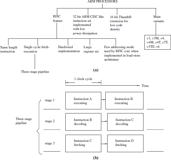
Figure 15.1 (a) ARM Processor Features and Variants of ARM Processor and (b) Features of Pipeline Processing Shown by Three Stage Pipeline in ARM7 Family of Processors
Single Cycle Operations in ARM
ARM performs thirty-two-bit processing for addition, subtraction, multiplication, multiplication with accumulation in the sum in the single cycle in sophisticated precision applications. It performs a single cycle multiplication. It completes division in 2 to 12 clock cycles.
Parallel Pipelines in ARM
ARM is a superscalar processor. It means that it has parallel pipelines. The performance becomes nearly m-times in m-parallel pipelines in the superscalar processor. Instructions are executed in the parallel pipelines. The performance becomes nearly n-times in an n-stage pipeline. Therefore, performance improves nearly n × m times in the superscalar processor.
Pipelining is facilitated when each instruction fetch is in a single cycle, decoding in single cycle and executing in the single cycle. A pipeline is used for processing such that at an instance more than one instruction is the different stages of the pipeline. Figure 15.1(b) shows a three-stage pipeline as in the ARM7 processor. The stages in a three-stage pipeline are (1) fetching an instruction, (2) decoding another instruction and (3) executing another.
Example 15.1
Pipelining gives about n-times greater performance in MIPS (million instructions per second) for the same clock speed and same architecture implementation of sophisticated precision applications. Two pipelines give about two times greater performance than that of a single pipeline.
RISC Architecture in ARM with CISC Features
An RISC has memory accesses by load and store architecture. It means the following:
- Variables and memory addresses first load into the registers by LD instruction, then
- the operations are performed using the registers by an instruction using ALU instruction and then the result is saved first in registers, and then
- stored back in the memory by ST instruction.
RISCs have large number of registers and fixed length instructions. RISC has few addressing modes during implementation (not necessarily during coding). They execute most instructions in single cycle. Instruction decoder (ID) connects to a hardwired implementation of each instruction. RISC gives greater performance in MIPS for the same clock speed than CISC in which instructions execute in variable a number of cycles and use control ROM. [Refer Nicholas P. Carter and Raj Kamal, “Computer Architecture and Organisation”, 2nd Special Indian Edition, Schaum’s Outlines, TMH, 2010 for details.]
Memory Architecture
The memory architecture is Princeton architecture in ARM7 and Harvard in ARM9. Figure 15.2(a) shows an overview of the memory organization in ARM-family MCUs.
- Processor can operate on the words as per initialization for their alignment at memory addresses.
- A word alignment can then be in big endian (least significant byte stored as higher bits (address 3) of a word). Word alignment can be in little endian (least significant byte stored as lower bits (address 0 of a word). Address 0 is an even address and the address 4 means the address of word that is next to next even address. Address 3 means address before the next to next even address (next to next odd address).

Figure 15.2 (a) Overview of the Memory Organization in ARM Family MCUs and (b) Overview of the CPU Architecture and Programming Model of Registers, Address and Data Buses. [Buses for Data and Address Separate in ARM9 and Same in ARM7]
Example 15.2
- 68HC11 has always 16-bit word byte 0 (lower byte) at a higher address and byte 1 (higher byte) at a lower address. [Big-endian mode.]
- The 8051 has always word alignment in the little endian mode—16-bit word byte 0 at a lower address and byte 1 at a higher address and 80196 always has little endian mode for double word (32-bit) and word (16-bit).
- The ARM can be programmed at initialization as little endian or big -endian for long word (64-bit), word (32-bit) and half-word (16-bit).
3. Princeton architecture processor stores program(s) and data in the same memory and makes it easy to reuse an instruction after a modification in the data part at the instructions within a program. ARM 7 has Princeton architecture for program and data memories.
4. Data have to be fetched continuously from successive addresses as a stream of bytes (or words) for an instruction in high- performance computing. For example, an array or matrix elements may have to be stored and fetched from successive addresses. Harvard architecture-based processor can access data and program memories at the same instant by using separate address and data accesses from the program and data memories. ARM 9 has Harvard architecture for program and data memories.
CPU Architecture
Figure 15.2(b) shows the CPU architecture. ARM processor core architecture is 16/32-bit RISC architecture. The processor operates on 32-bit words at an instance and can also operate separately on each byte of a word called byte 0, byte 1, byte 2 and byte 3.
Example 15.3
- 8051 MCU has a programming model that is based on A and B registers and four register banks of eight bytes each. When an ISR executes only program counter register save on the stack and on return pop from the stack automatically. Programmer saves the A and B and the registers of present bank for using registers of present bank in the new ISR using PUSH instruction for each. Alternatively, programmer re-defines the bank for using registers of another bank and are used in the new ISR. The saved registers are popped after the return using POP instructions.
- 68HC11 MCU has a programming model that is based on 8-bit ACCA, 8-bit ACCB, ACCA and ACCB used as 16-bit ACCD, and 16-bit IX and IY index registers in only one set of nine registers. When an ISR executes these nine registers save on the stack and on return pop from the stack automatically.
- A set of registers gives a programming model to a programmer. ARM processor has a distinct programming model. It is characterized by a large set of 16 general-purpose registers. Program counter is as one of the registers (r15) and CPSR and SPSR as two other registers [Fig. 15.2(b)].
Figure 15.2(b) shows registers, address and data buses to show the RALU operations in ARM-family MCUs [RALU means ALU with operations on registers only]. Table 15.1 gives the structural units and their uses in ARM architecture. Following are the model features:
- ARM7 and ARM9 support 300 MIPS when the die size is 0.13 μm. CPU supports sixteen 32-bit registers, r0 to r15. These form a general-purpose register (GPR) set.
- ALU operations are the register-based arithmetic and logic unit (RALU) operations.
- RALU does 32-bit add, subtract, reverse subtract, multiplying and multiplying with accumulate operations. It has a barrel shifter (multi-bits left or right shift or rotate).
- A GPR can function for computations as well as for index register for indirect addressing to memory in an instruction.
- 32/16-bit ARM instruction set feature is CISC with load and store architecture. Implementation is RISC. No RALU operations take place through a direct reference to the memory but through indirect reference. Operand in load and store architecture must first be loaded in CPU registers, operated and then saved to memory.
- 32-bit memory space is continuous with no segments.
- There are two modes of the processor—user mode and supervisory mode. The OS (supervisory SVC) mode is facilitated by the SWI instruction (software interrupt instruction). For supervisory mode functioning there is a separate register set (bank) in ARM7 and 9.
TABLE 15.1 The Meaning and Uses of the Structural Units Shown in Block Diagram
| Term | Full form | Use |
|---|---|---|
RALU |
Register Arithmetic Logic Unit |
CPU is a three-address machine with two source operands and one destination operand.a |
r0 to r14 fifteen registers |
Thirty-two bit fifteen general-purpose registers (GPRs) |
For source and destination operands during RISC implementation of the instruction. (Refer Fig. 15.2(b) right side blocks.) |
r15 (PC) |
Program Counter as GPR |
The register r15 is 32-bit program counter and it can also be used in computations as source. (Refer Fig. 15.2(b) rightmost side.) |
CPSR |
Current Program Status Register for each Process Mode |
CPSR.31, CPSR.30, CPSR.29 and CPSR.28 bits are N, Z, C and V flags (flags set on a negative result, zero result, carry or borrow during operations and overflow on arithmetic result overflow, respectively). |
SPSR |
Saved Program Status Register |
Saves Program Status Register from CPSR on branch and link (routine call) and SPSR can be stacked for each processor mode. |
IR |
Instruction Register |
Instruction Register to hold the current instruction opcode from dour byte queue. |
ID |
Instruction Decoder |
Instruction Decoder register to decode the IR opcode bits and activate the appropriate signals for hardwired implementation of instruction at IR. |
Condition Test Branch Logic |
Condition Test and Branch Logic |
Additional circuit to test the flags and initiate appropriate program flow path by branching. |
32 × 32 and 32 × 32 + 64 MAC |
32-bit multiply and 32-bit multiply and accumulate (MAC) |
Variant M of ARM have these units. (32 × 32 + 64 MAC units are needed for DSP and control applications). |
a A source operand (one RALU input) in RALU operations is first loaded, can also be first operated with rotate or shift instructions, can be either from register or register + memory or an 8-bit immediate operand. [A register indirectly indexes the word at the memory.] Another RALU input is from a source operand from a register. Result of RALU returns to a destination register. [Refer Fig. 15.2(b) middle for RALU and common bus for sources and destination from the general-purpose register set r0 to r15.]
Context Switching
Real-time interrupt response is fast because of provision for fast context switching. The fast context switching is present in ARM because of the sets of large registers. A new set (or bank) is used by called routine. Only the set or subset pointer needs to be used when switching to a routine. ARM has large register sets.
Assume that 8 registers r0–r7 and a status register are being used by a routine. The routine is interrupted and an ISR starts; now if the ISR uses another fresh set (or bank) of r0-r7 and status register, then context switching is fast. This is because there is no need to save previous routine parameters in r0–r7 and status register.
Interrupt Vectors
Interrupt vectors start from memory address 0 in ARM7. Four-byte address of each interrupt vector is stored there. Interrupt vector table starts from address 0 in ARM7 and ARM9. Interrupt vector table can be moved to another address using a control register in Cortex M3.
Interrupt Service
Interrupt servicing by IHR (interrupt handling routine) takes place after saving of return address in a register (r14), SPSR saves the CPSR bits, the CPSR bits to show which interrupt servicing taking place and PC becomes equal to the address at the interrupt vector. IHR restores CPSR from SPSR and clears the interrupt-disable flags and restores PC using instructions when return takes place to the foreground program.
Example 15.5
ARM7 follows banked shadow register exception (interrupt) model. It means that in supervisory mode, a separate bank is allocated for the supervisory mode programs r0–r7, current and saved program status register (CPSR and SPSR), link register (r14) and program counter (r15). The SPSRs are stacked if new ISR calls another routine. The SPSR returns to CPSR when there is return from the ISR.
ARM Variants in architecture
ARM has the following variants of architectures:
- vl – ARM1, v2 – ARM2, v2as – ARM3, and ARM250, v3 – full 32-bit addressing for both data and code ARM6, ARM7, ARM8 and Amulet 1, v3M–ARM6, ARM7 and ARM8, v4–Strong-ARM, ARM9, v5–ARM10, VFP1–ARM10, v6–ARM11 some variants for high floating point performance (single-precision and double-precision floating point arithmetic) on typical algorithms used in graphics and DSP.
- Thumb (T variants), which uses 16-bit Thumb® subset of instructions for high code density. It loses the conditional instruction execution part of the opcode in the instructions. It can address the first eight registers of the processor only. Thumb-2 version gives mixed mode capability. It means CPU can inter-work between Thumb and ARM modes.
- Long multiply instructions (M variants), four extra instructions that perform 32×32: 64 bit multiplication result when multiply instruction executes. 32 × 32 + 64:64 bit instruction means that the result (add multiplication result with 64-bit) when a multiply-accumulate instruction executes.
- Enhanced DSP instructions (E variants). [32×32: 64 operation means a 32-bit register value multiplies with another 32-bit register value to get 64-bit multiplication.]
- Jazelle version ARM architecture executes Java codes fast due to Java accelerator core as internal coprocessor.
- ARM 11 core used in ARM1176JZ(F)-S has an 8-stage pipeline and deploys ARMv6KZ architecture. It has Thumb, Jazelle DBX, (VFP) and Enhanced DSP instructions. It uses a variable amount of caches. It uses MMU and TrustZone memory protection unit. It finds applications in Apple iPhone. Samsung’s ARM11 versions are S3C6410 and S3C6430.
15.3 ARM7
ARM 7 TDMI™ architecture has the following features:
- Uses 0.25-μm and less die-size. Very small die size facilitates low voltage operations, and low power consumption. (A very small power consumption measure is MIPS/Watt.)
- Gives high performance of 300 MIPS at die size = 0.13 μm.
- Uses HCMOS technology. Has fully static operations, which means MCU clock can be reduced to 0 since it is fully complementary MOSFET based.
- There is a large register set consisting of sixteen 32-bit registers.
- There is a three-stage pipeline (pipelining means processing, memory and other systems can operate continuously) (Fig. 15.1(b)). (A Pentium has a five-stage pipeline.)
- There are 232 addresses for 4G bytes linear address space.
- There is a 32/16-bit RISC architecture (called ARM v4T), which has 32-bit ARM instruction set and a 16-bit Thumb instruction subset as extension.
- Thirty two-bit RALU and high-performance multiplier.
- There is a common internal bus for the address and data of thirty-two bit in ARM7. Thirty-two bit Princeton architecture bus and bus interface for the 32-bit data and instructions (ARM9 has Harvard architecture).
- Instructions process data with 8, 16 and 32-bit data types (byte, half-word and word).
- There are two types of requests for interrupts—Fast interrupt request (FIQ) and interrupt request (IRQ). Here, fast means high priority.
- Banked shadow registers are present. When the system interrupts to supervisory mode, a separate bank is allocated for the supervisory mode programs r0–r7, current and saved program status register (CPSR and SPSR), link register (r14) and program counter (r15),
- Coprocessor interface exists to connect coprocessors, like DSP processors and Java accelerators.
- The ARM memory interface has the speed-critical control signals, which are pipelined (control signals implement system control functions with standard low-power logic and facilitate fast local access modes by using the DRAMs).
- Extensive debug facilities [like embedded ICE (in circuit emulator), RT (real-time) debug and on-chip JTAG interface units exist.] JTAG provides direct high-speed access to the MCUs internal units (registers and control unit).
- Interface for direct connection to embedded trace macrocell (ETM).
- It supports Thumb instructions for 16-bit operations and for enhancing code density.
15.4 ARM9
ARM9 has Harvard architecture. ARM9 has the separate instruction and data cache memory. It has separate instruction and data buses. It has a five-stage pipeline compared to three in ARM7. It provides faster load and store due to more stages in pipeline. ARM9 gives higher performance than ARM7.
ARM9 supports the Thumb instructions like ARM7. ARM 9 T, E and J versions support. ARM 920 has 16 kB instruction cache and 16 kB data cache. ARM 940 T has memory protection unit. ARM supports Jazelle DBX (Direct Byte-code execution). The byte code in Java execute directly.
15.5 ARM-BASED MCUS
ARM Core-based MCUs
ARM embedded microcontrollers (MCUs) are single-chip microcomputers with the ARM architecture at CPU. ARM core-based MCUs based on ARM7 and ARM9 are widely accepted for applications needing high speed and performance in MIPS per Watt. The instructions use the byte, half-word (16-bit) and word (32-bit) for operations.
Example 15.6
AT91ASM9263EJ-S™ (E means DSP instructions extended instructions, J mean Jazelle Java accelerator version. It executes ARM/Thumb instructions. It has 16 kB plus 16 kB instruction an data caches. It has MMU (memory management unit). It gives performance of 220 MIPS for 200 MHz clock. It has embedded ICE, embedded trace macro-cell (ETM) and nine 32-bit bus-matrix. 28.8 Gbps is total on-chip bus bandwidth. It has 128 kB internal ROM and 80 kB SRAM. It has single cycle access and maximum bus matrix speed. It has DMAC, LCD controller, system controller, advanced interrupt controller, debug unit, two real-time timers, USB2.0, programmable frame capture, image sensor interface, two graphic accelerators, two synchronous serial control channels and three channel 16-bit timers. It operates at 1.08 V to 1.32 V. The peripherals derive at 2.7 V to 3.6 V. Further details are at Atmel Web site http://www.atmel.com/products/AT91/.
There are a number of ARM-based MCUs. Table 15.2 lists the ARM7TDMI ™ architecture feature MCUs.
Analog Devices ARM-based MCU is ADuC7026. ARM Cortex M3 based MCU is ARM Cortex-M1 from Altera. Atmel (http://www.atmel.com/products/AT91/) manufactures AT91 single chip controller, which has ARM9 as core in AT91RM3400. AT91 industrial controllers are AT91SAM7A11x CAN and AT91SAM7A24x CAN. [CAN stands for standard bus called Controller Area Network bus. The CAN is widely used in industry and in automobiles for networking the embedded controllers.] Refer http://www.e-lab.de/ARM7/AT91SAM7A2.pdf for a description of architecture.
An Atmel MCU is Atmel AT91SAM7S128. AT91RM3400 MCU from Atmel has ARM9 architecture plus SRAM + boot ROM, loads from an external SPI data flash. ARM9 with advanced RTOS compatibility like in STR720 is in AT91RM9200. It has 16 kB SRAM, 128 kB preprogrammed (AT91 boot ROM, SDRAM controller, JTAG interface, debugger, four UARTs, I2C master, SPI Master/Slave, USB Host and USB/Client, Ethernet, 3 x SSC (Synchronous Serial Controller), 6x timers, Compact Flash, Smartmedia MMC Card, SD Card and Burst Flash Controller.
A manufacturer of ARM7TDMI™ based MCUs is ST Microelectronics (referred as ST in the following descriptions in this Chapter). (http://st.com and http://www.arm.com/news/5135.html). ST manufacturers ARM based MCU chips (and cores), it integrates ARM7 TDMI ™ in STR71x (STR710, STR711, STR712) and STR720 derivatives, which are the high- end 32-bit single-VLSI MCUs.
An ARM9-based MCU from ST Microelectronics is ST STR912FW44. STR 10 and STR20 MCUs are also listed. Figure 15.3 shows 16/32-bit ARM-based flash STR710 microcontrollers with USB and CAN.
The ARM-based low cost and high performance Philips MCUs are low power LPC2114 and LPC2124. Philips MCUs are now made by Nexperia. Their architectural features and devices are also listed in Table 15.2. Another MCU is from Nexperia (Philips) LPC2148.
An ARM-based MCU S3C2410X01 is manufactured by Samsung. [http://www.pocketpccentral.net/help/samsung2410.htm]. It is widely used in PocketPC. [PocketPC means a PC that can be kept in a pocket and has mobile applications.] The S3C2410X01 is developed using a low-power, simple, elegant and fully static design. It is particularly suitable for cost-sensitive and power-sensitive applications. Also, S3C2410X01 adopts a new bus architecture. An outstanding feature of the S3C2410X01 is its CPU core, which is a 16/32-bit ARM920T RISC. (The ARM920T implements MMU, AMBA BUS and Harvard cache architecture with separate 16 kB instruction and 16 kB data caches, each with an eight-word line length.) By providing a complete set of common system peripherals, the S3C2410X01 minimizes the overall system costs and eliminates the need to configure additional components. A Samsung S3 based MCU is S3C44B0X. Table 15.2 lists the MCU features.
ARM MCUs are also available from Freescale and Texas Instruments. These are MAC7101 and TI TMS470R1B1M, respectively.
Figure 15.3 STR710 16/32 Bit ARM-based Flash Microcontrollers with USB and CAN

(Source http://www.st.com/stonline/products/support/micro/arm/str7/10-htm.htm with Courtesy and Permission of ST Microelectronics)
TABLE 15.2 ARM7TDMI™ Architecture Features along with Additional Features in STR 10, STR 20, LPC21x4 and S3C2410x01

a ST STR 710 and STR 720 derivatives.
b Harvard Architecture, a memory complier, external I/O microprocessor, AMBA (advanced microcontroller bus architecture) MCU, PLL for clock generation, 1.8 V internal, 1.8 V/2.5 V/3.3 V memory, 3.3 V.
c Highest performance embedded flash memory in 128-bit wide zero wait-state flash.
d MMU (memory management unit) allows running of the RTOS such as Linux, WIN-CE and QNX.
e Combined data and instruction caches and write buffer increase the execution speed and reduces memory bandwidth.
f Combined SDRAM and Cache for higher optimum performance.
g I2C (1-ch multi-master I2C-BU S/1-ch I2S-BUS controller), Touch screen interface, I2C BUS interface, SD 1.0 Host. h Additionally on-chip generator with PLL, watchdog timer and an RTC with calendar function.
i Also the HVQFN64 9 mm × 9 mm packaging.
15.6 ARM CORTEX-M3
Cortex-M3 processor has ARMv7-M architecture in addition to the following:
- It has a small core footprint. [Footprint means number of gates used in the core for similar instruction set of the core.]
- It gives high code density. It thus requires smaller memory for the code. It has small pin count.
- It has low power consumption.
- Harvard memory architecture.
- Excellent integration of the peripherals/SRAM through memory protection unit.
- Three-stage pipeline with branch prediction.
- Single cycle multiply.
- Two to twelve cycle signed/unsigned divide.
- Unaligned data storage programmability.
- Atomic bit manipulation. These instructions are required for wireless networking and serial transmissions of the bits. [Atomic means interrupt only after completing the bit manipulation.]
- Supports sleep mode.
- 1.25 Dhrystone MIPS per MHz clock cycle,
- Thumb®-2 instruction set architecture.
- Debug port configurable by serial wire or JTAG.
- DWT [data watch points (break points) and trace].
- FPB (flash path and break point unit). It has six program breakpoints and two data-fetch break points.
- ETM (embedded trace macrocell) interface. It is used for tracing the real-time instructions.
- Exceptional system response mechanism for the interrupts. This is because it deploys a NVIC (nested vectored interrupt controller). The NVIC supports nesting (stacking) of interrupts. Therefore, an interrupt of low priority can be preempted by exerting higher priority. It also supports dynamic re-priority allocations. Interrupts that are being serviced are blocked from further activation until the interrupt service is completed.
- Interrupt latency is 12 cycles in contrast to ARM 7, which has 24 to 42 cycles of interrupt latency. There is excellent deterministic interrupt behaviour.
- NVIC also integrates with the timer for the system ticks. It is a 24-bit count-down timer. It generates interrupts at regular time intervals. It thus gives system clock to run RTOS and timer for scheduling the tasks.
Details are in data sheets at http://www.arm.com/pdfs/Cortex_M3_DS.pdf. Applications are use as the cores for application microcontrollers, wireless networking, automobile and industrial control systems.
Configurable NVIC (Nested Vectored Interrupt Controller)
ARM 7 has two interrupts FIRQ/IRQ. Cortex M3 controls one NMI (Non-Maskable Interrupt) and 32 general-purpose physical interrupts using NVIC. There can be 8 levels of priority for preempting the low priority tasks by the higher priority tasks. It can be configurable between 1 and 240 physical interrupts with up to 256 levels of priority. Interrupt Vector table (IVT) locates at 0 address at the processor reset. IVT is re-located using a control register to another address. IVT is used to get the ISR address. When an interrupt takes place, r0–r3, r12, r15 (program counter), r14 (link register) and status register (CPSR) are pushed on to the stack automatically using the data bus. When there is return automatically these are retrieved. This is similar to 9 registers push and pop on the stack in 68HC11. The instruction bus retrieves the address from vector table at the same time slot. Thus, interrupt handling is fast. Inter-interrupt latency is six cycles, which are required for instruction fetch for the ISR. The interrupts can be tail-chained in case of back-to-back interrupts from same priority levels.

Cortex-A9 gives performance of 2.5 DMIPS/MHz. A9 has the VFP, Jazelle, DBX, Thumb-2 versions. It issues out-of-order instruction in the superscalar pipelines. [Out-of-order issue means that the instructions which don’t need result of previous instruction are inserted first in the pipeline stages.] ARM Cortex cores support Jazelle RCT (Runtime Compilation Target). RCT gives the efficient just-in-time (JIT) compilation and ahead-of-time (AOT) compilation with Java and other execution environments.
15.7 ARM INSTRUCTION SET
The ARM architecture is such that the 32-bit ARM instruction set and 16-bit Thumb® instruction subset both can be used. The instruction set extends to provide support for Java acceleration (Jazelle™). Instruction set also extends to provide support for security-coding features (TrustZone™).
15.7.1 32/16-bit ARM Instruction Set
The following are considered in an instruction-set:
- Instruction types
- Number of operands in the instruction
- Whether Instructions are of fixed length or variable lengths and
- Addressing modes.
The ARM has a large number of registers and instructions of fixed length. Each instruction is of 32-bit in the ARM instruction set. There are 16 registers, r0 to r 15. r15 functions as PC.
An instruction has op-code bits and operand bits. Absolute addressing means use of 32-bit address in the instruction operand. Therefore, absolute-(extended) addressing and direct-addressing instructions are not present in the ARM as the length of each instruction is 32-bit. Absolute address can be computed in a register by arithmetic addition or subtraction using the PC address from r15 and offset (as immediate operand) between current instruction address and desired absolute address.
Absolute address computation at a register r is by a pseudo instruction ADR r, addr, where addr are lower 12-bit for the 32-bit address.
One of the RISC instruction-set characteristic is load and store architecture. The ARM instructions are also such that the variables and memory addresses must first be loaded into the registers and then arithmetic or logic operations are performed using the registers and then the result should be stored in the memory. The arithmetic and logic operations are performed using register addressing. Load and store operations are performed using indirect and indexed addressing.
Example 15.7
Implementation of the ADR pseudo instruction is by implementing instruction SUB r, r15, #&byte_ offset, where 12-bit byteoffset is Address- r15 and r15 has the current program counter at a 32-bit address. (#& means the immediate operand is a hexadecimal and # means decimal value.) Addressing modes that are present in the ARM instruction set are as follows.
(1) Register Addressing: All operands are within the register itself.
Example 15.8
MOV r1, r2. MVN r1, r2 instruction. These mean (r1) ← ( r2) and (r1) ← NOT (r2). The second one means move r2 or complement of r2 bits into r1 (r2 bits do not change). (Note that logic operation NOT as well as MOV is combined instruction, MVN).
Example 15.9
ADD r1, r2, r3 add the source operands r2 and r3 bits and execution result is at the destinationoperand r1.
(2) Immediate Addressing: Second source operand can be an immediate operand. Immediate operand is of fewer-bits. For example, 8 bits in case of an ADDGT instruction, which adds if the conditional test is successful, 12-bits in case of an ADD with no condition tests. ADD r6, r7, #8 adds r7 and 8 and the result is in r6.
(3) Indirect Base and Indexed Addressing: It is the major mode for load-store architecture as direct absolute addressing is not provided. The following are the types of indirect addressing modes. In all the types the assumption is that all 16 msbs are 0.
a. A byte or half-word or word address is pointed by the indirect address in a GPR.
Example 15.10
LDR r1, [r2] instruction loads r1 from the memory address pointed by r2. If r2 is 1000 1000 1000 1000, then r1 will load the 32 bits from memory address 1000 1000 1000 1000. The r2 and r3 remain unchanged.
b. A byte or half-word or word address is pointed by the indirect address obtained by subtracting two registers of GPR set.
Example 15.11
LDR r1, (r2, – r3) instruction loads r1 from the memory address, which is as per r2 – r3. (If r2 is 1000 1000 1000 1000 and r3 is 1000 1000 0000 0000, then r1 will load the 32 bits from r2 – r3 = 0000 0000 1000 1000. The r2 and r3 remain unchanged.)
c. A byte or half-word or word address is pointed by the indirect base address by adding GPR with an offset as immediate operand. This mode is indirect addressing by base plus 12-bit byte offset (like base-relative or index relative in 80x86 processor).
Example 15.12
- LDR r4, [r5, #9] instruction loads r4 from the memory address pointed by r5 + 9. (Ifbase address at r5 is 0000 0000 1000 1000, then r4 will load the 32 bits from memory address 0000 0000 1001 0001. The r5 remains unchanged.)
- STR (r5, #&0C), r4 instruction store r4 32-bits to the memory address pointed by r5 + 12.
d. There is an indirect addressing mode by index plus offset with post auto indexing.
Example 15.13
LDR r4, [r5], #8 instruction loads r4 from the memory address pointed by r5 and then adds the offset 8 to r5. (If r5 is 0000 0000 1000 1000, then r4 will load the 32 bits from memory address from 0000 0000 1000 1000 and make 0000 0000 1001 0000 by adding offset = 8d at the immediate operand.) The r5 remains changed for the use of r5 next time. This is called auto post indexing.
e. There is an indirect addressing mode by index plus offset with pre-auto indexing by using an operator.
Example 15.14
- LDR r4, [r5, #8]! instruction loads r4 from the memory address pointed by r5 after first adding (due to operator ! in the instruction) byte_offset 8 into r5. If r5 is 0000 0000 1000 1000, then r4 will load 32 bits from memory address 0000 0000 1001 0000. This is because of the operator first adding byte_offset = 8 into r5 value before using r5 to point to memory address for loading r4. The r5 changes before the present time use of r5. Byte_offset can be a 12-bit immediate operand. The mode is called auto indexing with base register also updating before fetching.
- LDR r15, r1! instruction loads r15 to the memory address pointed by r13 after first adding (due to operator ! in the instruction) the offset 1 into r13. (Offset 1 means address change of 4 because a 32-bit word = 4 bytes. If r15 is 0000 0000 1000 1000, then r15 will load to the 32 bits from memory address from r13 after making r13 = 1000 0000 0000 1100 if r13 earlier = 1000 0000 0000 1000. This is because of an operator first adds offset = 1 (means 4) into r13 value before using r13 to point to memory address for loading r15. The r13 is changed before the present time use of r13. This is called auto indexing with the base register also updating before fetching).
All instructions have condition-test field in 4 msbs at 32-bit instruction. When cond = 1110, the condition test is ignored and instructions are always executed irrespective of flags. The instruction types are as follows.
15.7.2 Data Transfer, Bit Clearing and Masking Instructions
These are three types of data-transfer instructions: (a) Move (conditional or unconditional and with or without the shift or rotate) from first to second register, (b) Load from a memory address source operand indirect or indirect with offset or (c) Store to destination operand memory address indirect or indirect with offset.
MOV and MVN are move and move the complement to a register and/are register-to-register move instructions. Table 15.3 in Section 15.7.2 gives the instruction format. Second source operand can also be shifted or rotated before using the source in the comparison operations. Flags can be changed as per the S-bit in the instruction. Move can be conditional or unconditional as per cond 4-bit field in the instruction (Table 15.3).
TABLE 15.3 Instruction Format for 32-bit Move or Compare or Arithmetic Add or Subtract or Logic Operation Instructions
| Bit(s) | Field Name | Use |
|---|---|---|
b31-b28 |
cond |
Specifies test condition. |
b27-b26 |
00 |
Major opcode specifies one of the four group of operations move or compare or add or subtract or logic operations. |
b25 |
X |
X = 1 means that 12 lowest significance bits specify immediate 8-bit operand, which is used after rotation specified by 4 bits b8-b11; = 0 means that 12 lowest significance bits specify source operand register which is used for shifts in cases 1 and 2 |
b24-b19 |
opcode |
4-bit Minor opcode specifyies the specific operation in the group |
b20 |
S |
S specifies CPSR flags need change or no change from the operation. |
b19-b16 |
Rn |
First source operand Rn. = r4 if bits b15-b12 = 0100 and r15 if 1111. |
b15-b12 |
Rd |
Destination register Rd. = r9 if bits b15-b12 = 1001 and r15 if 1111. |
b11-b0 |
format as per b25 (X) (b0-b11 are for operand2) |
If X =1 then b11-b8 specifies rotate right instruction and b7-b0 immediate operand. b11-b8 = 0000 means no rotation, b11-b8 = 0001 means rotate right 2 times, b11-b8 = 1111 means ROR 30 times. Immediate operand is 32-bit with 24 msbs = 0s and lsbs b7-b0. |
LDRB, LDRH, LDRSH and LDR are the load byte, half-word, half-word signed and word-load instructions, respectively. These are indirect memory address-to-register load instructions, in Section 15.7.1(3). STRB, STRH, STRSH and STR are byte, half-word, half-word signed and word store instructions. These are register-to-indirect address based store instructions (signed half-word means extend the sign 0 or 1 at b15 into the bit b16 up to bit b31).
There is a single data (8 or 32-bits) swap (conditional or unconditional) between register and memory. Swap takes place by a memory read and memory write. Instruction specifies source (Rm), destination (Rd0) and base (Rn) registers. Rn gives the swap address. Data bits of Rm are written at the memory address. Old data bits at memory are written at destination register Rd).
Block Data Load and Store Instructions LDM and STM do the block registers load and store from or to the memory, respectively. LDM and STM are mainly used for popping and pushing when performing stack operations using these instructions.
Data and Bit Clearing and Masking During Manipulation BIC r1, r2, r3 performs find bits after logic AND between r2 and complements of r3 bits and moves the result in r1.
Assume that r1 is to acquire bits of r2 after clearing the bit specified in r3, and then BIC is used. This is assuming that r3 is 1100 1110 0111 1111. The r3 functions as a mask register. This means, BIC instruction will clear all bits except b7, b8, b12 and b13 bits from the r2bits to put the result in r1. Assume r2 = 1111 1110 1000 1000, then BIC r1, r2, r3 will result in r1←0011 0000 1000 0000. If r3 is 1000 0000 0000 0000 only then b15 will clear in r1 using r2 and r1 will become 0111 1110 1000 1000.
15.7.3 Arithmetic operation instructions
The basic arithmetic instructions are as follows:
- There are the destination, first source and second source operands. Second source operand can also be shifted or rotated before using the source in the arithmetic add and subtract operations.
- There are arithmetic instruction operations of ADD, ADC (add with C flag), SUB, SBC (subtract with C flag used for borrow) and MUL. (8051 does not have SUB subtract without borrow.)
Example 15.16
MULL (32 × 32: 64) is to multiply a long instruction. These arithmetic instruction operations can be defined as conditional or unconditional and defined with or without shift rotate manipulation of second source operand.
3. ARM has instructions for reverse subtraction (first source from the second and with C flag used borrow. This is given because second source can be bit manipulated before being used in an ARM arithmetic instructions.
4. There can be conditional or unconditional MUL and MLA in a 32 × 32 multiply (32 × 32: 32) and multiply with add instruction. MUL can multiply only. MLA multiplies followed by add (bit 0 or 1 in the opcode specifies it). There can be multiplication with or without change of the condition flags (S bit 1 or 0 specifies it). The signed or unsigned multiplication is only 32-bit long.
5. There can be conditional or unconditional in MULL and MLAL instructions. These are 32 × 32 multiply long (32 × 32:64) without or with add instruction, respectively. MULL and MLAL are specified for signed or unsigned operation by U (1 or 0) bit at the opcode for multiply or multiply and add by A (0 or 1) and to change and not to change flags by S bit (1 or 0).
6. These operations are used in control and signal processing systems.
Example 15.17
MLA r1, r2, r3, r4 will multiply r2 and r3 and add the result with r4 and accumulate the result in r1. MLAL r1, r2, r3, r4 will multiply r3 and r4 and add the result with r1(H) r2(L). Sixty-four-bit result accumulates r1(H) r2(L) itself after adding the multiplication of r3 and r4.
7. ARM variant M and ARM7TDMI have instructions MLA and MLAL. These are for MAC 32 × 32 multiply and 64-bit accumulate by summing.
Example 15.18
MLAL helps in evaluating a result by summing a multi-term finite series consisting of products of coefficients and variables. Some examples are y = c0 + i.a + j.b + k.c and y1 = c1 + c1.x + c2.x2 + c3.x3 + … MLAL helps in matrix or multi-term series multiplications.
8. An arithmetic operation like a data transfer operation can be made conditional. The flags of CPSR, N, Z, C, V collectively reflect a condition. The condition tests are at an earlier operation for tests for HI or LS (unsigned higher or not higher, C = 1 and Z = 0 or C = 0 and Z = 1), LT (less than, N ≠ V), GT (greater than N = V and Z = 0), GE (signed greater than or equal, N = V), LE (signed less than or equal, Z = 1 or N ≠ V), PL or MI (plus or minus, N = 0 or 1), NE (not equal, either greater or less, Z = 0), EQ (equal, Z=1), CC or VC (C or V flag clear = 0 on carry or overflow) and CS or VS (C or V flag set = 1 on carry or overflow).
Example 15.19
SUBEQ r1, r7, #5 means that if previous comparison showed operands as equal, then destination operand in r1 will equal result of subtraction of r7 and byte 0x05.
15.7.4 Logic Operation Instructions
The logic operations are as follows:
- EOR is logical XOR between two source operand registers and result is in a destination operand register.
- ORR is bit-wise logical OR between two source operand registers and result is in destination operand register.
- AND is bit-wise logical AND between two source operand registers and result is in destination operand register.
15.7.5 Data and Bit Manipulations during Move, Arithmetic, Data Swap, Branch and Exchange Instructions
There are no separate shift or rotate instructions. These operations are done using second source operand before the RALU is used in an operation. Bit-manipulation of second source in RALU instructions is as follows:
- ROR is rotate right and RRX is rotate right extending to carry bit. ROR rotate right shifts of the msbs and fills the vacated msb positions by the lsbs (least significant bits).
Example 15.20
16-bits half word ROR by eight times will change 1100 1110 0111 1111 to 0111 1111 1100 1110 (whether C is 0 or 1) and when C = 0, RRX will change through carry to 1111 1111 1001 1101 and C becomes 0 again and when C = 1 then to 11111111 1100 1110 and C changes to 0. (Now consider the example of 16 msbs for simplicity. Actual operations are 32-bit operations. RRX rotation use 33 bits, 32-bit second source operand and C-bit at CPSR and ROR 32 bits only.)
2. ASR for arithmetic right fill sign bit at msb (0 or 1) at the msbs, which vacate on shifting.
Example 15.21
ASR shifts 12 times and this will change 1100 1110 0111 1111 to 1111 1111 1111 1100 and when it shifts 10 times will change 0100 1110 0111 1111 to 0000 0000 0010 0111.
3. LSL (or ASL) and LSR for logical (or arithmetic) shift left and logical shift right fill 0 at the lsb and msb positions, respectively, that vacate on shifting.
When the LSL shifts 12 times then 1100 1110 0111 1111 will change to 1111 0000 0000 0000 and when LSR shifts right 10 times, will change 0000 0000 0011 0011.
Comparison and Test Instructions Comparison is by hypothetical subtraction. The second source operand can also be shifted or rotated before using the source in the comparison operations. Flags affect on comparison. Only the N, Z and V affect in test. Compare can be conditional or unconditional as per cond 4-bit field in the instruction (Table 15.3). The instructions are as follows:
- CMP is for comparison of two source operands and none of the registers affect. Only the CPSR flags C, N, Z and V are affected.
- CMM is for comparison of two source operands, second one after negation. It means a hypothetical addition. None of the GPR registers are affected. Only the flags C, N, Z and V are affected.
- TST is for hypothetical bit-wise AND operation in which N and Z are affected and V = 0.
- TEQ is for hypothetical bit-wise XOR operation with similar outcomes as previous instructions.
15.7.6 Program Flow Control Instructions
Four types of program flow control instructions (no flag in the CPSR affect) for a jump or call by branch or branch and link are as follows:
- Unconditional Branch PC Relative Instructions: B # addr is an unconditional branch instruction called branch target. PC offset is four times addr because offset 1 means first word and the next word is always after four bytes.
- Conditional Branch Instructions: This is a conditional branch related to PC after condition test. These tests are the same as specified earlier for arithmetic instructions.
- Conditional or Unconditional Branch and Exchange (Call) Instruction: BX is an instruction in which PC register r15 is exchanged with a register. Return from the call is by another BX at the end of the routine.
- Conditional or Unconditional Branch and Link (Call) Instructions: A branch followed by link is related to PC.
Example 15.23
BL #addr, where addr is 16-bit value and is the conditional or unconditional branch instruction called branch and link. PC offset is four times addr because offset 1 means one word and next word is always after 4 bytes. r14 saves the current PC as a return address. It is advised to store r14 at the stack area in memory when (a) r14 is to be used for anything other than return in the linked routine or (b) multiple nested calls are to be made. Register r13 is conventionally used to point to the top of the stack. (In ARM set, it is convention and in Thumb subset, it is implicit).
Example 15.24
STR r13!, r14 will save r14 on stack and increment r13 by four for next word store to stack top. We can save local variables after branching using STM r13!, rn–r14 on stack and increment r13 by twenty four for next work stored to top. (rn–rm means a list of registers between rn to rm. When n = 9, there are 6 registers because m = 14 in the above instruction.)
5. There is no return instruction. Return (after Call) instruction can be MOV r15, r14. It will return the return address pointer at r14 into the PC address in r15. One return instruction can be LDM to restore the registers from the stack.
15.7.7 SWI interrupt control instruction
It is an unconditional-cum-conditional SWI software-interrupt instruction. Format is cond SWI for 8 msbs. (It does not need operands; remaining 24-bit lsbs are irrelevant as far as execution of the instruction is concerned.) After interrupt, the SWI handler code is called, provided none of the other exceptions (interrupts) have been flagged. The handler can use the 24 bits for the suffix parameter and number. After stacking the link register (return address for PC) an SWI handler code can call another SWI by BL instruction. The OS (supervisory SVC) mode is facilitated by the SWI instruction.
A software interrupt instruction is SWI <suffix> <number>. The <suffix> and <number> have 24 bits. The suffix and number are irrelevant during execution of SWI instruction. Suffix is used for programming the passing of the pointer for the parameters of the interrupt handler. Number is used as interrupt number of the SWI handler (ISR) by the programmer. The number points to the ISR address.
SWI par_num_24 is a software-interrupt instruction and switches the processor to run the SVC (supervisory codes) at an SWI handler. This is a simple facility, but is used widely for catching and throwing errors and handling errors and exceptions using the handler. Many Operating System (OS) functions are provided by SWIs. A RISC OS uses the SWIs.
Example 15.25
SWI has opcode of 8-bit. The 32-bit instruction for using SWI. Consider SWI b23……..b01. When it executes, the program starts from interrupt vector for SWI. The program first reads the value of b23….b0 bits. The program then uses part of the bits (b0 to bn−1) as interrupt handler number to jump to service routine (task) to be executed. The program then uses part of the bits (bn to b23) as suffix to get pointer for the parameters to be used by the task.
Example 15.26
Instruction for throwing an exception in high-level language is executed by SWI in low level language. When an abnormal condition occurs during computations, the SWI is used. The catch function in high-level language is the ISR (SWI handler) which is executed on throwing the exception. SWI is used widely with appropriate suffix and number for catching and throwing errors and handling errors and exceptions using the handler.
Example 15.27
Operating System (OS) functions initiate the running of the tasks (or threads or ISRs). A new task initiates and runs by calling an SWI handler by the OS function. OS function executes an SWI instruction with appropriate suffix and number or BL.
15.7.8 Formats of 32-bit Instruction
- Move, add, subtract, logic or compare instruction 32-bit format is cond 00 X opcode S Rn Rd operand.
- Table 15.3 gave the instruction format for 32-bit move, compare, arithmetic add, subtract and logic operation instructions.
Table 15.4 gives the format of multiplying long and multiply and accumulate long (32 × 32:64) instructions. Table 15.4 also gives the format variation in multiply and multiply and accumulate (32 × 32:32) instructions. (a) MULL and MLAL Instruction format are cond 00010 U A S RdHi RdLo Rs 1001Rm. The operations are RdHi-RdLo ← Rm × Rs and RdHi-RdLo ← RdHi-RdLo + Rm × Rs. (b) MUL and MLA Instructions 32-bit format is cond 00010 U A S Rd Rn Rs 1001 Rm. The operations are Rd ← Rm × Rs and Rd ← Rm × Rs +Rn. [Rs means source register. Hi means higher byte of register. Lo means lower byte of register.]
TABLE 15.4 Instruction Format for 32-bit Arithmetic Multiply and Multiply and Accumulate
| Bit(s) | Field name | Use |
|---|---|---|
b31-b28 |
cond |
Specifies test condition. |
b27-b23 |
opcode |
Opcode specifying multiply long when 00010 and multiply when 00000. |
b22 |
Ua |
1 means signed, 0 means unsigned. |
b21 |
A |
1 specifies multiply and accumulate and 0 means multiply only. |
b20 |
S |
1 for change in condition flags in CPSR and or 0 means no change. |
b19-b16 |
RdHi |
32 msbs (higher 32 bits word of 64-bit double word result) at register RdHib. |
b15-b12 |
RdL0 |
32 lsbs (lower 32 bits word of 64-bit double word result) at register RdLo Destination lower word registerc. |
b11-b8 |
Rs |
32 bits word source register Rs. |
b7-b4 |
1001 |
Specifies MUL or MLA or MULL or MLAL instruction’s minor opcode. |
b3-b0 |
Rm |
32 bits word register Rm source b21. |
a Equals 0 in MUL and MLA.
b Equals Rd in MUL and MLA.
c Equals Rn in MUL and MLA.
Instruction Format of Load and Store Instructions
Instruction format of load and store instructions is cond 01 X P U B W L Rn Rd offset. Moreover, P = 1 means pre-indexing and 0 means post-indexing. U = 1 refers to up (add offset) and equals to 0 refers to down (subtract offset). B =1 means byte transfer and equal to 0 means word transfer. W = 1 is write back of the address to or from the base in store or load and W = 1, 0 is no write back. Write back is of post or pre-increments. Increment is 4 for a word and = 1 for a byte transfer. L = 0 store and 1 and load. Rn is the base register when it points to memory data for load or it is a register in store instruction. Rd is the destination register. It points to memory the data for store instruction otherwise it is a register. The meaning of X bit is similar to that in Table 15.3. If X = 1, then b11-b0 12-bit offset specifies rotate and an 8 bit immediate operand, else b11-b0 specifies the shift-rotate and register Rm. The offset means offset to the base register. When W = 1, r15 is not specified as base register.
Instruction Format of a Half-word Load and Store Instructions
Instruction format of a half-word load and store instructions is cond 000 P U 0 W L Rn Rd 00001SH 1 Rm. SH = 00 means swap instruction, 01 means unsigned half-word, 10 means signed byte and 11 means signed half word. Rm is not specified as r15 register for offset. When r15 is used as source and a data transfer is of a half-word, then the stored half-word will be from an address PC+2.
Instruction Format of SWP Instruction
SWP (data swap between memory and register) instruction format is cond 000010 B00 Rn Rd 00001001 Rm. B = 1 means as per cond field perform byte swap, else word swap. Rm is source register, Rd is destination register and Rn is base register. Data bits of Rm are written at the memory address as per pointed the base register. Old data bits at memory are written at Rd.
Instruction Format of LDM and STM Instructions
Instruction format of LDM and STM is cond 100 P U S W L Rn Register-list. P = 1 means indexing and equal to 0 means post auto indexing. U = 1 is add offset and 0 means subtract offset. S = 0, no CPSR load or force user mode and S = 1 means use CPSR or force user mode. W = 1 means write back of the address to or from base and 0 means no write back. L = 0 means store and equal to 1 means load. Rn is the base register to point to the block memory source for load and destination for store. Register list gives the list of registers to be loaded or stored.
Instruction Format of Branch and Call (Branch and Link) Instructions
Conditional or unconditional BX Instruction format is cond major-opcode 24bits Rn. Rn and r15 exchange as per condition test field cond specification.
Conditional or unconditional B and BL instruction format is cond 101L offset. L = 1 means branch and link, else branch only. Offset is a 24-bit two’s complement signed number, which is made 26 bits by left shift twice and the sign at b25 extended into b26 to b31.
Instruction Format of SWI Instruction
SWI instruction format is cond 1111 as 8 msbs and the remaining 24 bits are irrelevant for instruction execution (but may be relevant for the interrupt handler (ISR)).
15.8 THUMB® INSTRUCTION-SET EXTENSION
There is a 16-bit instruction subset called 16-bit Thumb® subset of the most commonly used 32-bit instructions. The ARMv4T and later ARM architecture variants added the 16-bit Thumb instruction set. It enables compilers to generate more than 30–35% (compared to 32-bit ARM code) of the compact code and thus 30% less power dissipation while using the 16-bit memory data bytes and Thumb set. It also has the advantages of the 32-bit ARM processor with regard to system performance. Run time expansion of the Thumb instructions takes place into 32-bit equivalent ARM instructions. This has been achieved due to the following:
- There is a T-bit at CPSR in architecture that supports the Thumb set also. Setting T-bit in CPSR can always switch from ARM to Thumb and vice versa. T-bit is set using assembly instruction code 16. T-bit is reset using the assembly instruction code 32. Therefore, commonly used instructions can be use in a 16-bit instruction format by first using instruction code 16.
- All ARM instructions have condition test field of bits at 32-bit instruction. Many instructions may not require conditional flags. Thumb instructions do not have a condition field that takes 4 bits.
- ARM mov, add, subtract, compare and logic operations provide for the rotation on immediate operands and shift or rotate on the second source operand. Such instructions may not need shifting or rotation too often. 16-bit Thumb instructions do not have the fields for rotate or shifts because that takes 12 bits for second source operand out of 32-bit instruction (Table 15.3 last row).
- ARM have 16 registers, each of 32 bits. Most of the times, the eight registers can suffice for using as GPRs. Hence, each register is defined by 4 bits in ARM instructions. Thumb set replaces the 4-bit by 3 bits for a register. Further, having a common source-cum-destination register (as in a two address machine like 80x86) further reduces the number of bits. This enables 16-bit instruction format for mov or add or subtract or compare or logic operations. Thumb instructions have 3-bit register field each for source- cum- destination and source 2 register in the instructions.
- Consider ARM instruction field X P U B W L. There are six bits for setting the options. Each Thumb instruction can have only a few options. This enables fewer instructions for load and store operations using the 16-bit load and store instructions.
- Recall ARM instruction field S. This gives two options. One option is to change the flags and another is for no change in flags. Thumb set has only one option, change the flags.
Thumb instruction set assumes the following model for programming:
- The registers r0 to r7 give a lower register set. Most instructions that use these suffice. Registers, r8 to r15 give higher register set. Few instructions like MOV, LDM, PUSH or POP can access r0–r15 GPRs by 4 bits for each register.
- r15 E= PC as in ARM. Few instructions use PC as the source or destination for operands.
- r14 is LR (link register) for return address after BL instruction. Few instructions can use it.
- r13 is an implicit stack pointer. All instructions use it as a stack pointer in Thumb. [ARM uses r13 not as implicit stack pointer but convention is that r13 is taken as stack pointer in ARM set.]
- Data processing, conditional branch and condition control instructions change the CPSR.
Thumb instruction set support following data types and memory alignment:
- Supports 8-bit, 16-bit and 32-bit data types.
- The memory is half-word aligned. Each offset increase or decrease is by two addresses.
15.8.1 Thumb Instruction Set
Data Transfer Instructions LDRB, LDRH, LDRSH and LDR are the load byte, half-word, half-word signed and word load instructions. These are indirect memory address-to-register load instructions. STRB, STRH, STRSH and STR are the store byte, half-word, half-word signed and word store instructions. These are register-to-indirect memory address store instructions. (Signed half-word means extend the sign 0 or 1 at b15 into the bit b16 up to bit b31.)
- LDR/LDRB/LDRB/SRTB Rd (Rn, #offset-5) loads or stores using Rd and index register Rn for memory address. Index registers bit + 5-bit offset defines the memory address for loading bits (or storing) into (or from) Rd. Offset-5 bits are shifted twice (means multiplied by 4) for LDR or STR and not shifted for LDRB or STRB. Instruction format is 011B L #offset-5 Rn Rd. B = 1 means byte operation and equal to 0 means word operation. L = 1 means load into Rd and L = 0 means store from Rd.
- LDRH/STRH Rd (Rn, #offset-5) loads or stores half-word using Rd and index register Rn for memory address. Index registers bit + 5-bit offset defines the memory address for loading bits (or storing) into (or from) Rd. Offset 5 bits are shifted once (means multiplied by 2) for LDRH or STRH. Instruction format is 1000L #offset-5 Rn Rd. L = 1 means load into Rd and L = 0 means store from Rd.
- LDRB/LDRH/STRB/STRH {S} Rd [Rn, Rm] loads or stores byte or half-word using Rd and base register Rn for memory address. Base registers bit + Index register bits defines the memory address for loading bits (or storing) into (or from) Rd. S = 1 means subtract and equal 0 means add index. Instruction format is 0101opcode-4 Rm Rn Rd. Opcode 4 bits specify the LDRB/LDRH/STRB/STRH {S} instruction for the load or store, byte or half-word and add or subtract index.
Load/store Instructions Using SP and PC (r13 and r15) in Branched or Linked Routines
- LDR Rd [PC, #offset-8] loads in Rd the r15 (PC) + 8-bit offset. Offset 8 bits are shifted twice (means multiplied by 4) for LDR. Instruction format is 01001 Rd #offset-8.
- LDR/STR Rd [SP, #offset-8] loads into Rd the r13 (SP) + 8-bit offset. Offset-8 bits are shifted twice (means multiplied by 4) for LDR or STR. Instruction format is 1001L Rd #offset-8. L = 0 means store to memory address from Rd and 1 means load into Rd.
Block Data Load and Store Instructions LDM and STM do the block registers load and store from or to the memory, respectively. Memory is indirectly addressed. LDM and STM are used for popping and pushing when performing stack operations.
- LDMIA/STMIA Rn!, reg-list loads multiple indexed auto from memory addresses indexed by Rn with autoindexing or stores multiple indexed auto to memory addresses indexed by Rn with post autoindexing. reg-list specifies the list of registers. For example, r0-r4 means five registers from r0 to r4. Instruction format is 1100L Rn reg-list. L = 0 means store to memory address using auto indexed index register Rn and 1 means load from the memory into the listed registers by 8-bits. (Registers and addresses map to ARM set.) An example is STMIA r0, {r13–r14} pushes the r13 and r14 (SP and LR) of the user program. Storing is by post indexing increments and loading is by pre incrementing r0.
- POP <reg-list {,R} pops into reg-list using SP r13 as memory address pointer. SP decrements by four on POP before the operation. PUSH <reg-list {,R} pushes from listed registers using SP r13 as memory address pointer. SP increments by four on each push operation. Instruction format is 101111 L R reg-list. L = 0 means PUSH to memory address from listed registers and 1 means POP into listed registers. R = 1 means include r15 (PC) and R = 0 means include LR (r13). Register list starts and ends with a register specified by 4 bits.
Arithmetic Operation Instructions Following are the basic arithmetic instructions. Note that the Thumb modelled register is of 3-bits each.
- ADD/SUB Rd, Rn, Rm: There is a destination operand (Rd) and first source (Rn) and second source operand (Rm). Second source operand cannot be shifted or rotated before using the source in the arithmetic add and subtract operations. (This is unlike an ARM.) The instruction is 000110A Rm Rn Rd. A = 1 means add and equal to 0 means subtract.
- ADD/SUB Rd, Rn, #immediate-3: There is a destination operand (Rd) and first source (Rn) and second source is immediate operand of 3 bits at the instruction. Instruction is 000110A immediate-3 Rn Rd. Option field A = 1 means add and equal to 0 means subtract.
- ADD/SUB/CMP Rd/Rn, Rm: There is a destination operand (Rd) cum first source (Rn) and second source is register of 3 bits at the instruction. Instruction is 010001 opcode-2 D M Rm, Rd/Rn. Option field D = 1 means 32-bit operation. Opcode-2 bits specify ADD or SUB OR CMP.
Arithmetic Instructions Using SP and PC (r13 and r15) in Branched or Linked Routines
- ADD/SUB SP, SP, #immediate-7 is to add result in source cum destination register SP (r13). SP ¨ SP + 7-bit immediate operand. Instruction is 10110000 A #immediate-7. The option field A specifies addition or subtraction.
- ADD Rd, SP/PC, #immediate 8 is to add result in destination Rd. Rd ¨ SP or PC + 8-bit immediate operand. Instruction is 1010 R Rd, #immediate-8. The option field R specifies SP or PC.
Logic Operation Instructions Format is Op Rd/Rn, #immediate-8. The first source-cum-destination operand is a register and second source is an immediate operand of 8 bits at instruction. Instruction is 001 (opcode-2 bit) Rn/Rd immediate-8. Opcode is of 2 bits for logical operations. Logic operations can be EOR, ORR or AND.
Data and Bit Manipulation Instructions There are separate shift instructions, these are the operations done using source operand and then the RALU is used in an operation and a register is at the destination register operand. Bit manipulation of source in RALU instructions is as follows:
- Opcode #Sh Rn, Rd: There is source Rn and destination operand Rd. The instruction is 000 (opcode-3 bit) #shift-4 Rn, Rd. Opcode is of 3 bits for the LSL, LSR and ASR operations. Shift is defined by 4 bits at the instruction.
- Opcode Rn/Rd, Rm/Rs: There are source cum destination Rn/Rd and source registers for the operation. The instruction is 010000 (opcode-4 bit) Rd/Rn, Rs/Rm. Opcode is of 4 bits for the shift and rotate operations.
Comparison Instructions Comparison is by hypothetical subtraction. Only the flags affect on comparison. The instructions are listed.
- ADD/SUB/CMP Rd/Rn, Rm instruction is used for comparison. Opcode-2 bits after 010000 (msbs) specifies ADD or SUB OR CMP. CMP is for comparison of two source operands and none of the registers affect but only the CPSR flags, C, N, Z and V affect.
Program Flow Control Instructions Four types of program flow control instructions (no flag NZCV change in the CPSR) for jump and call by branch or branch and link are as follows:
- Unconditional and Conditional Branch Instructions: B <cond><level-8> is a conditional or unconditional (when cond =1110) branch instruction, called branch target PC relative. An eight-bit level defines the offset 16-bit value for branch address of target into r15. Offset scales to half words relative to PC.
- Unconditional Branch instruction: B <level-11> is an unconditional (when cond =1110) branch instruction, called branch target. An 11-bit level defines the offset 16-bit value for the branch address of target into r15. Offset scales to half-words relative to PC and thus PC = PC+ (offset <<1). (offset <<1) means level-11 value left-shift once and then make up to offset 16-bit value. Left-shift by 1 makes PC offset equal to two times level because offset 1 means one half-word two bytes in Thumb (next word is always after 4 bytes in ARM instruction set).
- Unconditional Branch and Exchange (Call) instructions: BX H Rm 0000 is an instruction in which PC register r15 is exchanged with a register Rm. Return from the call is by another BX at the end of the routine. H = 1 means PC branches to half-word scaled (16-bit instructions) instructions and . H = 0 means PC branches to word scaled (32-bit instructions) instructions.
- Unconditional Branch and Link (Call) instructions: A branch and link is relative to PC. BL #lev-el-11 is an unconditional branch instruction, called branch target. Instruction format is 1111H #level-11. When option H = 0, then r14 LR= PC + (offset <<12). (offset <<12) means level value left-shifts twelve times and then makes up to 32-bit value. LR means link register to hold the return address from the subroutine. When H = 1, PC = PC+ (offset <<1) and LR = old-PC + 3. The LR (r14) saves the current PC as a return address. It is advised to store r14 at the stack area in memory when (a) r14 is to be used for other than return in the linked routine or (b) multiple nested calls are to be made. Register r13 is always used to point to the top of the stack in Thumb. Branched and linked routines can use (i) load/store instructions for SP and PC (r13 and r15), (ii) ADD Rd, SP/PC, #immediate 8 can be used to save PC and SP after adding the needed bits to these, (iii) ADDSUB SP, SP, #immediate-7 sets the stack pointer r13, (iv) STR r13!, r14 will save r14 on stack and increment r13 by 4 for next word to stack top. We can save local variables after branching using STR r13! Rn will save Rn r14 on stack and increment r13 by 4 for next word to stack top and (v) LDM and STM can be used to stack the registers.
There is no return instruction. Return (after call) instruction can be MOV r15, r14. It will return the return-address pointer at r14 into the PC address in r15. One return instruction can be LDR to restore the registers from the stack. (There is no decrement instruction like r13! post-increment for LDR.)
15.8.2 Thumb Instruction Format
Thumb instructions are 16-bit instructions. These instructions are fetched from the memory and execute on 32-bit ARM processor. Therefore, ARM processor when used with Thumb instruction set gives less code density. These are decompressed to their equivalent ARM instructions before sent into ID (instruction decoder) and run using hardwired internal-architecture. Thumb set permits a large (32-bit) instruction set as well as a 16-bit instruction set for most of commonly used programs. There is code compression by Thumb instructions.
Table 15.5 gives an exemplary format. It is for the instruction format for arithmetic instructions. For example, ADD r4, #data8 will add 8-bit data 8 into r4. ADD r4, #128 will add 128 into r4. Thumb 16-bit instruction will be 6 C 80 H 011 01 100 1000 0000. The bits b8-b10 are for source-cum-destination register. Bits b0-b7 are immediate operand and bit b13 is for immediate addressing mode. Note also that the add instruction takes an additional operand when decompressed. Decompressed 32-bit format will be 1110 (condition code) 011 01001 (minor opcode) 0 (S bit) 01000 (S bit) 0100 0000 (rotation) 1000 0000. We are now using condition code bits (though unconditional operation) for unconditional add, rotation bits (though no rotation, first source register bits in decompressed format).
TABLE 15.5 Instruction Format for 16-bit Thumb Subset Arithmetic Instructions
| Bit(s) | Field Name | Use |
|---|---|---|
b15-b14 |
Major opcode |
Major opcode 3-bits specify which of the four-move or compare or add or subtract. |
b13 |
Major opcode X - bit |
X = 1 means that 12 lowest significance bits specify immediate 8-bit operand which is used after rotation specified by 4 bits and 0 means that 12 lowest significance bits specify source operand register which is used for shifts. |
b12-b11 |
Minor opcode |
Minor opcode 2-bits for specify add-subtract or logic operation For example, 01 specify ADD not ADC when major opcode = 00. |
b10-b8 |
Rd |
First source-cum-destination operand register by 3-bits. r0 is specified by b10-b8. |
b7-b0 |
Second source or immediate byte |
Specifies 8-bit immediate operand value or the registers for first and second source operands or second source register with operations on that. |
How does the ARM know if the instruction it is running is a Thumb instruction or a regular ARM instruction? The ARM contains a special state bit that tells the CPU whether to expect a compressed Thumb instruction or the standard ARM instruction. This bit is toggled with its own instruction, BX that must be inserted into the code every time a programmer or compiler wishes to switch between the Thumb mode and the standard ARM mode. An obvious result of this is that there is some overhead to switching between modes and thus it is probably not a good idea to switch to Thumb unless it saves more than two instructions of the equivalent ARM code.
15.8.3 ARM/Thumb Inter-working
T-bit at CPSR gives the support for inter-working with 16-bit Thumb set and 32-bit ARM. T-bit in CPSR can always switch from ARM to Thumb and vice versa using assembly instruction code 16 and code 32, respectively. When working with 16-bit Thumb set, execute the instruction code 16 or set T-bit in CPSR. When switching to 32-bit arm set execute the instruction code 32 or reset T bit in CPSR. ARM and Thumb code each execute in their own processor state as ARM PC at r15 increments by 4 and Thumb by 2.
15.8.4 Thumb 2
Recent Thumb 2 core technology gives a mixed mode capability. [http://infocenter.arm.com/help/index.jsp?topic=/com.arm.doc.ddi0338g/ch01s02s01.html] Thumb-2 gives improved program flow instructions. It gives new 16-bit Thumb instructions. These are derived from ARM instruction equivalents and give new 32-bit ARM instructions for improved performance and data handling. Cortex and ARM1156T2-S™ are the examples of the ARM processors that use the Thumb 2 set.
It defines a new set of 32-bit instructions that execute along side traditional 16-bit instructions in Thumb state. ARM processor then gives performance as well as reduced code density. The new Thumb-2 core technology retains the compactness as well as code compatibility and supports earlier 32-bit ARM instructions software.
Thumb-2 is a superset of the Thumb instruction set. [Any code compiled for ARM v6 Thumb will also run with the Thumb-2 instruction set.] Thumb-2 introduces 32-bit instructions that are intermixed with the 16-bit instructions. Thumb-2 code density is same as Thumb and performance near to the ARM set.
New Thumb 2 Instructions
32-bit ARM Thumb-2 instructions are placed in-between BL and BLX instructions. The instruction length and functionality is determined by first 16-bit [halfword (hw1)]. If the hw1 instruction is decoded as being 32-bits long, then the processor fetches second halfword (hw2) of the instruction from the instruction address plus two.
Thumb-2 introduces a new conditional execution instruction, IT, that is a logical if-then-else function. After IT executes, the next 1 to 4 instructions become conditional. There is support to co-processor access, handling exceptions, DSP and multimedia instructions. There are additional CBZ (compare and branch on zero) and CBZ (compare and branch on non-zero) instructions.
15.9 EXCEPTION HANDLING IN ARM
ARM processor architecture provides for exception (interrupt) handling and has the following features:
- It provides for multiple valid exceptions at the same time during the execution of an instruction and their handling by the processor core.
- Handles the exceptions after completing the execution of the current instruction.
- Handling the exceptions is according to following priorities in the descending order: (1) Reset, (2) Data Abort, (3) FIQ, (4) IRQ, (5) Pre-fetch Abort (pre-fetch means advance fetching of bytes from memory into catches. Pre-fetch abort occurs when branching and pre-fetched codes or data in caches is thus no longer valid) and (6) SWI or undefined instruction (illegal opcode). The undefined instruction and SWI do not occur at the same time. This is because the exception from both is due to an instruction entering the execution stage of the ARM instruction pipeline. They are thus mutually exclusive. They have the same priority.
- Prioritization of exceptions occurs when multiple exceptions are valid at the same time. It differs from an actual exception handler code, which when run should not cause further exceptions. Infinite exception loops can destroy link register contents so return to return address for the handler does not occur.
- SWI interrupt handler codes can call another SWI interrupt handler.
- User program has the codes for the Undefined_Excpt_Handlers, SWI_Excpt_Handlers, PAbort_Excpt_Handlers, DAbort_Excpt_Handlers, IRQ_Excpt_Handlers, and FIQ_Excpt_Handlers. Undefined_Excpt_Handlers handles the undefined exception. SWI_Excpt_Handlers handles the SWI interrupt and so on.
A program must ensure the following:
- Support for priorities assignment of the exception handlers (ISRs)
- Provision for passing of a parameter(s) to the handler
- Use of completely static (uses no global variables) by the handler
- Use of reentrant routine [Reentrant routine means that when there is return from interrupt, the program reenters into original state, which is just before the interruption.]
- Support to the early finish of an handler
- Calling chain of shorter handlers. This reduces the latencies of interrupts.
- Support for use of unlimited handlers
- Support to installation and use of exception-vector for an handler
Meaning of Throwing and Catching an Exception
When a program runs, a run-time exception (error or special run-time condition detected by CPU) can occur. Examples are as follows—illegal opcode, an access to protected memory, division by zero, array out of bound, URL not found exception when trying to connect to the Web using an URL. There can be other exceptions. The processor should then interrupt and run an exception handling routine. This action is called catching the exception.
An exception occurs due to some run-time condition detected, while an interrupt occurs due to the software interrupt instruction like SWI or the hardware or device (like timer) interrupt or certain pin or device assigned interrupt. Like interrupt vectors, the exception vectors are present as per the processor architecture. A vector address gives the address of user function (like ISR) for the exception handling. Like interrupt priorities, different exceptions can have different priorities.
Catching of a run-time condition, event or error follows the program vectoring to the exception handler (a routine or function executed like an ISR). The ISR is called on throwing an exception (interrupt) during execution of a function or program. Multiple exceptions are handled as per the priorities of the thrown exceptions.
ARM architecture provides for the exceptions. The exceptions are listed in Table 15.6. An SWI instruction execution or hardware interrupt from IRQ or FIQ also handles like an exception. Each exception handler executes like an ISR, the address of which is pointed by a vector address (prefixed as per the processor architecture). The program has the codes for the exception handler and initializes the vector address location. This action enables the processor to call the handler by taking a pointer from there.
TABLE 15.6 Exceptions and Interrupts in ARM
| Name | Priority | Use |
|---|---|---|
Reset |
Highest priority interrupt, always responded |
Initialize the system without saving any state or register, and disables FIQ and IRQ hardware interrupts. On reset, the handler program first initializes all interrupt sources, which needs initialization and thereafter FIQ and IRQ initialized when required. Program enters in SVC mode on reset. Reset handler must first set the stack pointers for all the other modes so that any exception occurring later can be handled. Reset handler must not have an exception from illegal opcode, SWI or a memory access occurs, though permitted by ARM. |
Data-abort |
Lower than Reset but has higher priority than FIQ |
In case the FIQ handler is being executed then return is to Data-Abort abort vector when this exception is pending. A Data-Abort exception disables IRQ interrupt to complete the handler routine. Data abort handler may however enable IRQ. Like Reset, handler must not have an exception from illegal opcode, SWI, though permitted by ARM. Suppose, there is pre-fetch abort exception (when data abort handler is at memory page not currently paged), then the abort handler re-enters. Therefore, the data abort handler must not throw pre-fetch abort exception or result in further aborts. |
FIQ |
Next to Reset priority. |
By default, the ARM prevents nested FIQ interrupts. An FIQ in exception (interrupt) sets the F and I bits at CPSR and thus disables automatically all IRQs and FIQs during the execution of the FIQ handler. FIQ handler when running can, however, re-enable FIQ or IRQ by resetting F or I out of some necessity of an application. FIQ handler (ISR) should therefore have a short run time like a data or prefetch or SWI handlers for reducing interrupt latencies. |
IRQ |
Next to FIQ data abort exception |
By default, the ARM prevents nested FIQ and IRQ interrupts. IRQs are therefore automatically disabled by setting I bit at CPSR during the IRQ handler run. IRQ handler when running can however reenable FIQ or IRQ by resetting F or I out of some necessity of an application. |
Pre-fetch abort |
Next to IRQ and FIQ |
Assuming that when an instruction is being executed, a read error fetch occurs, then a pre-fetch abort is thrown (flagged) when the Abort instruction reaches the execution stage at the pipeline and none of higher priority interrupts occur in-between. By default, the ARM sets the I bit and prevents IRQs during pre-fetch abort. Other exceptions can however be thrown and thus handled if required. |
SWI |
Next to all but above User code instruction |
When an instruction is fetched and decoded successfully, and during that none of the other exceptions are thrown (flagged) and the instruction is an SWI instruction, then the ARM enters SVC mode. SWI handler now executes. |
Undefined Instruction (Illegal Opcode) |
Same as SWI User code instruction |
When an instruction is fetched and decoded successfully, and none of the other exceptions thrown (flagged), and the instruction is however undefined in the ARM and is thus an illegal code, the ARM enters Undef mode. Undef handler now executes. Usually, Undef handler sends the instruction to any coprocessors at the system. If none are presented an error is reported. SWI and Undef have the same level of priority and cannot occur at the same instance. |
An SWI can call another SWI after storing LR at the stack and branching occurs for “child” SWI. SWI interrupts can be nested. SWI instruction sets the processor mode to supervisory and sets the PC to execute the next instruction from hexadecimal address at address &08! [=0x00000008]. When the processor is put into the SVC, r13 and r14 switch out and are replaced with r13_svc and r14_svc, respectively. The r14_svc sets to the return address after the SWI instruction. This links the calling foreground program. SWI functions like a BL instruction that links to the next PC address &08 (BL &08) but with space for some data (the SWI number). At this address, if instruction is LDR PC, &0000032C, then the SWI handler executes the codes from 0x0000032C.
Finding Interrupt Number
Using LDR r0, [r14, #-4] and processor gets 24-bits (for interrupt number) when executes BIC r0, r0, #0xFF000000. Using this number, a lookup table base address, and the r15 is loaded with appropriate value to branch to the corresponding routine (OS function, error handling function or caught (thrown) exception function).
Handling Exceptions
Handler will find using (r14 − 4) the 32 bits there and omit 8 bits for cond SWI and find remaining 24 bits. From it the SWI interrupt number bits parameter bits can be found. In this way, the SWI handler will be able to find the different exceptions thrown and handle these accordingly.
Consider program Example 15.1. It shows the exception handling in C.
Program Example 15.1.
Consider a C function declaration, void func_1 () throw exception_1 (“exception at ‘func_1’”). It specifies to the compiler that func_1 ( ) will be running in a function block ‘try’ as follows and can catch an exception of type (or class) Exception_1.
/* Some function or main functions, which return an integer, when no exception is thrown */
1. int funct_0 ( )
2. try
3. {/* Codes for the function func_1 ( ) */
4. funct_1 ();
5. } /* End of try block */
6. catch (Exception_1 excep0) /* Wait and runs when the exception excep0 of type Exception_1 caught*/
7. {/* Codes executes for the exception excep0 thrown by function func_1 ( ) */
8. /*The block can either terminate the program or return an integer to specify the exception that was caught and handled*/
} /* End of catch block. */
9. return 0; /* Return 0 if no exception caught during run of funct_1 () */
10. }
Note that function unexpected () should run if an unexpected exception is thrown. The unexpected () must not be permitted to throw and handle any exception but run only the exception expected from try block function, funct_1 () or the functions of the application.
15.10 DEVELOPMENT TOOLS
A development tool should support popular ARM-based MCUs—ST Microelectronics ST30, STR710 and STR720, Atmel AT91x, Philips (now Nexperia) LPC2104, LPC2105, LPC2106, NetSilicon NS7520 and NET+50 and cortex M3 in an IDE. The IDE must provide and support standard device databases. The IDE must provide accurate simulation and timing for the peripheral. The IDE must include flash programming and target debugging. A developer selects the tools, depending on the level of sophistication needed in a project. Table 15.7 gives the options.

a Needs library manager, linker/locator, monitor and PROM programmer evaluation board MC 2100 for Philips LPC21xx ARM MCUs.
b Make means integrating assembling, compiling and linking for the embedded application. Software embeds into the target hardware or system. Also, supports industry standard GNU tools for C compiler and ARM (ADS) Assembler.
c Keil Software Inc. ARM development tolls now taken over by ARM.
d Not using high-level language, multi-tasking, RTOS, and debugging tools.
e PK ARM from Keil will give RTXA-Tiny plus DKARM kit. Supports USB link and JTAG in PKARM and DKARM. Alternatively use CARM.
Eclipse IDE, GNU/GCC ARM Compiler, Cygwin, Zylin CDT and OpenOCD are also used. These are open source tools Keil is now an ARM company. For developing applications of ARM MCUs.
Example 15.28
Keil originally developed an RTOS named ARTX-ARM (Advanced Real-Time Kernel (executive) for ARM family MCUs). The advanced real-time kernel consists of the RTX Kernel, Flash File System and TCP/IP networking Suite. When ARM took over Keil, it is called RL-ARM or RTL-ARM. RTL stands for real-time library.
ARM μVision IDE
Section 12.4.1 described μVision IDE for 8051. μVision IDE for ARM has similar features. Picture 15.1 shows the screen menu of Keil IDE. The Keil Software manufactures the Keil ARM tools and options PKAARM and CARM have in-built ARM assembler Keil AARM and ARM C compiler Keil CARM. Keil also gives the development tools for the ARM MCUs.
Keil software development tools for the ARM7 TDMI architecture support every level of developer from the professional applications engineer to the student. The Keil ARM development tools support the most popular ARM7 derivatives.
The Keil μVision debugger is claimed to accurately simulate the on-chip peripherals (I2C, CAN, UART, SPI, Interrupts, I/O Ports, A/D Converter, D/A Converter and PWM Modules) in the ARM device. Simulation helps in understanding the hardware configurations. It reduces the development time needed in the setup problems by using the device database present at IDE for ARM.
Program Debug and Testing Using JTAG and Serial Wire Interface
Example 15.29
The Keil ULINK2 USB-JTAG Adapter connects the USB port of personal computer (PC) and USB port the target system [via JTAG (Joint Test Action Group), SWD (Serial Wire Debug) or OCDS (On-Chip Debugging System)]. It permits the program and debugs the downloaded programs at the target. [OCDS is a special method. It is used to program flash memory. It then debugs the programs running in system microcontrollers].
ULINK2 installs Windows USB drivers automatically. ARM Cortex-M3 based devices need Serial Wire Debug (SWD). It is also provided by ULINK. Real-Time Trace for Cortex-M3 is given by Serial Wire Viewer (SWV). It also provides NXP 2-wire debug interface (P89LPC952 and P89LPC954).
It has real-time agent. It gives memory read and write support. It gives serial debug output. It has flash memory programming algorithms. These algorithms can be configured by the programmer. Using the Keil μVision IDE/Debugger along with the ULINK2 adapter enables create, download and test the application software on the target hardware.

Picture 15.1 Keil IDE mVision3 Screen Menu (Photograph by Permission and Courtesy of Keil Software Inc.)
Atmel offers the following development tools. (a) Development boards for all Atmel’s ARM-based products, (b) Software including basic device drivers and application software layers and (c) Development tools include compiler, debugger, JTAG and ICE (In-Circuit-Emulators) interfaces, Real-time Operating Systems (RTOS), TCP/IP stacks and application-specific software objects.
ARM RealView® Developer Suite
An ST ARM-based MCU system can be developed using popular ARM RealView® developer suite. RealView developer suite is a registered trademark of ARM Limited. It enables developers to reduce system memory cost, through smaller code size and increased system performance, without a dramatic increase in power consumption. It has a targeted compiler, a targeted GUI debugger and the ST specific RealView ICE micro edition and JTAG run control device.
Example 15.30
RealView MCU development kit from Keil supports ARM7, ARM9 and Cortex-M3 MCUs. It gives industry-standard compilation tools and sophisticated debugging support. It includes IDE, debugger and simulator. It includes ARM ADS/RealView compilation tools for C/C++ and support GNU ARM compiler. It includes RT kernel RTX and detailed start-up code and flash programming algorithms for ULink.
Evaluation Board
An evaluation board means a board with ARM MCU device and other chips and components to enable downloading of the developed codes and evaluating the performance of the development system.
Example 15.31
ST provides an evaluation board, which is a complete development platform for the STR71x flash MCUs for development target. Picture 15.2 shows iSTR710-EVAL board. It consists of STR710FZ2T6 ARM7TDMITM device. It has the 2 × 16 LCD, LEDs, 10 serial communications SPI, UART (RS232C port), CAN, USB interfaces, and includes, piezo-buzzer and test-buttons to create a versatile stand-alone test platform. It enables rapid evaluation of the STR71x devices and available peripherals. It has high-performance 2 Mbits embedded flash with least random access time, 64 kB on-chip high-speed SRAM plus EEPROM. This enables development of large programs before custom hardware for a system is designed. It supports software development tools from ST, ARM, Ashling, GreenHills, Hitex, IAR and PLS. Picture 15.3 shows the evaluation board MC2100 for Philips LPC 21xx ARM MCUs.

Picture 15.2 Complete Development Platform iSTr710-EVAL Board for the STr71x Flash MCUs (Photograph by Permission and Courtesy of ST Microelectronics)
MC2100 has LPC2129 CPU. It has X-Tal of 60 MHz, prototyping area, JTAG interface, 32 kB on-chip RAM, 512 kB on-chip flash, LCD, Analog input potentiometer, analog output to speaker, 8 I/O port LEDs, serial port:2, CAN ports: 2, USB host, push-buttons, Ethernet 10/100 and SD card interface.
Example 15.33
Innovate (www.innovatyesolutions.net) has an Evaluation board for development. It has the following: CPU ARM926EJS architecture based AT91SAM9263. Operation: 200 MHz, Power management unit, NAND Flash: 64 MB, SDRAM: 64 MB, Ethernet Port 1: 100 Mbps, Serial Port; 2, USB Host: 2, USB Client: 1, CAN Port: 1; PWM signal 1: ADC 12-bit: 2, MMC/SD Card: 1, JTAG port: 1, JTAG interface: 1, Audio-in: 1, Audio-Out: 1, Keypad: 3×3, Display 8-segment: 2, Display TFT/LCD touch screen: 3.5”: 1, Jumper : J1, Expansion Interface: 1 and Wi-Fi support external module.
Software for the board are WinCE 5.0 and Linux 2.6.23. Other requirements are Flash programmer, tool chain for kernel compilation, eclipse-based IDE for application-development in Linux, documentation for guiding the user, developer and programmer and datasheets. These are provided with the evaluation board.
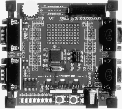
Picture 15.3 An Evaluation Board MC2100 for Philips Nexperia LPC21xx ARM MCUs (Photograph by Permission and Courtesy Keil Software, Inc.)
UDE (Universal Debug Engine) gives a flexible debug platform. It is available for ST10F16x, ST10F26x and ST10F280 architecture from ST Microelectronics and the ARM7 derivatives. It also works as 32-bit TriCore and the Infineon 16-bit architecture SAB C16x, C166CBC, C166S V2. It is a new debugger architecture and tool concept based on a customizable set of standard components and core specific add-ons. It supports the JTAG, breakpoints, stepping in ROM/flash and sets the complex event-trigger conditions without any external hardware or software resources.
15.11 PORTING DEVELOPED CODES IN ARM BASED SYSTEM
Process of porting the developed codes in a system is called burning the image. An image is a unique arrangement of pixels. Identically, an image, which is burnt (used for programming the flash or RIM) means unique words/bytes for the RTOS, codes, routines and data and these are placed at unique addresses in the target (evaluation board during development phase) flash or ROM or RAM.
Innovate kit described in Example 15.33 is used to port the images as follows:
- Host: Porting of image is done with the help of a host. Host can be a personal computer with Windows 2000 and above operating system or Linux RedHat 7 or 8 or 9. A Minimum of 500 MB free space is required. It should have a COM port. It should have terminal communication software (Minicom in Linux or Hyper terminal in Windows).
- Target: Target board is the evaluation board. It has RS232C cable for connection to the host. It has a cable for Ethernet. It has a jumper (J1) for starting and operations later.
- Configuring the Network: Allocate IP address automatically. IP of target is the same as of the host. Host is 192.168.1.56 and object board 192.168.1.55, network mask is 255.255.255.0 and broadcast IP is 192.168.1.1.
- Booting: UBoot download tool in windows is used or uboot.bin compiled file is used. Open the hyperterminal. Set the baud rate = 115200, parity number and flow control number.
- Enabling Download Functions from Host to Target: Remove the jumper J1. It enables download and debuggung.
- USB: USB serial bus at COM5 is connected from the target to the USB at the host.
- Installing Drivers: The drivers are installed after prompt ROMBoot> appears on the screen.
- Burning Kernel and File System: RUN SAM-BA.exe file. Look in folder for ROM Image. Select address 0c08000 and size for receive file = 0x1000 (4 kB). Select and open the file dataflesh_sam9263ek.bin. The files will be written in flash automatically. Open and select uboot. bin. The following actions take place: reset all counter registers, chip select 0 selected, switch to SPI IO mode register. wqit for data flesh ready. Press send button on screen. The uboot is written into data flesh.
- Close and Reset: Close SAM-BA, remove USB slave line and press K10 button for reset at the evaluation board. The start-up information appears at the hyper terminal.
- Writing Kernel and JFFSL File System in Linux: Steps for the kernel and JFFSL file system in Linux are as given in the manual. Download command is uboot> tftp 22200000 uImage to download at address 22200000.
- uboot> nand erase to erase the NAND flash memory.
- uboot>nand write 22200000 200000 to write into the flash.
- uboot>run ramdisk to write the files in RAM disk at flash.
15.12 PORTING LINUX IN ARM
Web site http://www.arm.com/products/os/linux_download.html is used to download the Linux for ARM platform. Boot loader U-Boot is taken from http://www.denx.de/wiki/U-Boot. U-Boot images are ‘‘.axf’ files. Linux images are “uImages”. The configuration files are plain text format files.
Linux Version for the ARM
Main Linux kernel is supported by ARM for the RealView Platforms and RealView tools and platforms. The Linux kernel images, patches, utilities and file system (http://linux.onarm.com/) images run the Linux on ARM processors and RealView platforms. The Linux 2.6 kernel version is available for ARM720T, 920T, 922T, 926EJ-S, ARM1136J(F)-S, ARM1176J(F)-S and ARM11 MPCore, Cortex-A8 and A9. http://www.arm.linux.org.uk/ and http://www.linux-arm.org/Main/WebHome provide patches, discussion groups and information.
Linux version of Linux runs on ARM processors with Memory Management Unit (MMU). The processors without MMU can run a modified version of Linux called uClinux. uClinux can also be downloaded from the above site. There are pre-built uClinux images for some ARM processors at the site.
Installation and Setup Procedures
Installation and setup procedures are available from http://www.linux-arm.org/LinuxReference/LinuxOnARMDev?redirectedfrom=Main.LinuxOnARMDev.
Download of Thumb-2 libraries and applications can be from http://www.linux-arm.org/LinuxReference/LinuxOnARMDev?redirectedfrom=Main.LinuxOnARMDev.
Peripherals
Linux 2.6 generates images using GCC 4.3.2 and GNU libc 2.8 compilers for the following peripherals: UART (PL010, PL011), Interrupt Controller (VIC, GIC), Ethernet (PL092), LAN9118, LAN91C111, USB, MMC, CompactFlash, Timers, L2C (220), KMI (PL050), RTC (PL030), VGA/LCD (PL110), AACI (PL041) and VFP.
15.13 ASSEMBLY AND C PROGRAMMING (GNU TOOLS)
Application Examples
Web site http://www.atmel.com/dyn/products/app_notes.asp?family_id=605 gives the application notes from ATMEL for the ATMEL ARM-based MCUs. Package for the software drivers and libraries to build any application for AT91SAM3U devices can be downloaded from the Web site. www.atmel.com. This package provides IAR 5.3, Keil and GNU support.
Industry standard for assembler and compiler is ARM AD5/RealView compiler. GNU tools for ARM are also available free. However, the codes developed using it are not optimized and a needed device support may not be there.
An ARM device (Analog Devices ADuC7020, Philips Nexperia LPC 2104, 2106, 2129, 2294, 2114, 2214, 2119 and 2129, Atmel AT91F40416, AT91M55800A, ST Microelectronics ST710 and ST720) may be difficult to set up and configure (Table 15.1). Keil AARM and Keil CARM are the assemblers and C compilers from Keil, which permit a programmer to choose the compiler and assembler to use. These enable (a) selection of a freeware GNU compiler, when the goal is to reduce development tools cost, (b) selection of an industry standard ARM AD5/RealView compiler when the goal is to use standard development tools and (c) selection of the Keil CARM C compiler when the goal is to generate programs for the ARM MCUs (the single-chip devices) such that an optimized code for that device generates from the object codes from the assembler/compiler. This compiler gives numerous exemplary programs, which help a programmer to get started with the most popular embedded ARM devices.
Web site http://www.keil.com/appnotes/list/arm.htm gives the application notes for 173:Implementing Interface DLLs for ARM Hardware Debuggers - Rev. 2,188:ELF/DWARF Output Format Used by Keil ARM Tools. 190:Using RealView MDK-ARM for Atmel AT91SAM7 Devices, 192:Using TCP/IP Examples on ARM Powered Evaluation Boards, 193:Migrating to MDK-ARM from RVDS, 194:Using the Real-Time Agent, 195:Developing HID USB Device Drivers For Embedded Systems, 197:Serial-Wire Debug and Realtime Trace on STM32 Devices, 200:Setting Up ULINK2 for LogicPD iMX LITEKIT, 201:Setting Up ULINK2 for LogicPD LH7A404 Card Engine and 202:MDK-ARM Compiler Optimizations.
SUMMARY
- A superscalar processor has more than one pipeline for processing. A pipeline has at an instance more than one instruction at the fetching, decoding and executing stages. Pipelining is done when each instruction fetch is in a single cycle, decoding in a single cycle, and executing in the single cycle. The performance becomes about n-times in n-stage pipeline. Superscalar processor performance enhances due to parallel pipelines.
- ARM MCUs can run in low power modes (Slow, Idle, Stop and Power-off).
- ARM has RISC architecture. RISC processors have few addressing modes—load and store architecture, large register set, and hardwired implementation of the instructions. Each instruction executes in single cycle and has same length.
- RISC gives higher performance in MIPS is of compared to a CISC.
- ARM is RISC processor with load and store architecture and a pipeline of three or more stages.
- ARM has sixteen 32-bit registers with r15 as PC, r14 as link register for return address and conventionally r13 as stack pointer.
- ARM7, ARM9 and ARM Cortex M3 are the architectures used in the ARM MCUs. The ARM MCUs have high performance with very small power dissipation.
- ARM architecture-based MCUs give high performance at small power dissipation. ST Microelectronics manufactures ARM MCUs, STR71x and STR720 derivatives and Philips manufacture LPC series. ARM CORTEX M3 is a recent ARM architecture. It has new features such as Embedded Trace Macrocell and Nested Vectored Interrupted Controller.
- ARM7 has Princeton memory architecture and ARM9 has Harvard architecture.
- Instructions have 8-, 16- and 32-bit data types. ARM can be specified to store the words (of 32-bits) and half-words in little-endian or big-endian mode.
- 32-bit instructions form a subset in which all instructions have condition test field, which uses N, Z, C and V flags; all instructions have rotate and shift and immediate operand or index register memory operand.
- 16-bit instructions form a subset, called Thumb instruction set, each instruction of which decompresses at run time into the ARM instructions.
- The processor can switch between 16-bit Thumb and 32-bit ARM instructions.
- Exceptions are the interrupt events caught at run time and which result in the execution of a handler like an ISR. SWI instructions are used to switch the processor to a supervisory mode and execute OS and error-handling exceptions.
- ARM IDE is used for project development.
- Linux can be ported on ARM boards.
KEY TERMS
ARM addressing modes: Addressing modes are register, immediate, indirect, indexed, auto-indexed.
ARM7TDMI™: ARM7 processor variant with support to Thumb instruction subset in instructions set of ARM, which gives smaller code density and decompress at run-time in the processor.
BIC: Bit clearing instruction using a mask. For example, BIC r0, r0, #0xFF000000 clears upper 8 bits in r0.
Cache: A fast read-write memory to pre-fetch instructions and data and to write back data at fast rate and which reads memory by pre-fetch and writes to slow external buses subsequently. Cache lets a processor run at fast speed through slower external memory buses. Cache stores in content addressable memory format. Address key and 64 or 128 or 256 bytes can exist in each line (entry) in cache.
CAN: A standard bus for controller area network to network the systems, for example, automobile systems. Child SWI: An SWI handler called by another parent SWI handler.
CISC: A complex instruction set computer processor, which has complex addressing modes, variable length instructions, different cycle times for executing instructions. Instructions implement using control memory and micro code engine.
Coprocessor: A processor interfaces to the main processor and executes special instructions or accelerates the throughput. Uses are for fast execution of floating point instructions. Java accelerator executes Java codes fast.
CPSR: Current Program Status Register for each process mode, NZCV four flags of it are used in condition test instructions, T-bit used for switching between Thumb and ARM instruction sets in a program.
Data abort: An exception thrown for data error.
Embedded fast flash: A flash memory in an MCU, in which sectors can be erased fast and bytes can be written fast.
Exception: An execution time condition of an instruction or an interrupt or error, which branch and links to the handler (ISR).
Exception catching: A term used in C program for running a function (handler) when an exception is thrown. ARM has SWI handler, which runs on catching an exception.
Exception handler: An ISR, which address is specified by a vector address and which runs to respond the exception.
Exception throwing: A term used in C and Java programs for activation of a run-time condition or error or interrupt. Exception thrown is catched. This runs a function (handler) or method. ARM has instruction SWI, to which is used in program throw an exception.
Floating-point: A data type, which permits use of decimal point and exponent. The data examples are 3.14159, −10.0000346, 123.5. 10-5.
Half-word: 16-bit data type stored at even and odd address pairs in memory.
JTAG: Joint Test Action Group standard interface to give direct high-speed access to the MCUs internal units (registers and control unit).
Link register: Register r14 used as return address when a program branches by BL or SWI instruction.
Load: Byte or half-word or word taken to register(s) from memory address(es).
Instruction format: A way to specify how the bits are arranged in an instruction or instruction subset.
MAC: Multiply and then add the result into the accumulating register. This helps in finding sum of the terms of a series. ARM MLA and MLAL instructions do the MAC operations.
MIPS/Watt: Million Instructions per second per Watt of energy dissipation. It is measure of processor performance at low power.
MMU: Memory management unit controls pre-fetch of instructions and data and write back.
Offset: The address which adds (or subtracts) to a base address. Offset value is found from immediate operands and depends whether access is taking place for a word or half-word address.
Pipeline: A line in which n-instructions can be at n-stages during the fetch-decode-execute cycles of the instructions.
Pre-auto indexing: Before memory access is by using index register, which first increments by 4 for a word.
Post-auto indexing: After the memory access in order to make next word access using index register, index increments by 4 for a word.
Pre-fetch: Fetching into caches from memory.
Prioritisation: Priority assignment to exceptions and interrupts.
Programming model: A model for using the CPU registers and other structural units.
Pseudo instruction: Instruction used by the assembler, but which is not a part of ARM or Thumb instruction set. Assembler converts it into ARM instruction.
RISC: A reduced instruction set computer (processor), which has fewer addressing modes, fixed length instructions, fixed cycle times for executing the instructions. Instructions implement using seperate hardwired circuit for each instructions.
Smart card interface: An interface for contact or contact-less communication with an MCU-based card. SPSR: Saved program status register.
Store: Byte or half-word or word taken from register(s) to memory address(es).
Superscalar processor: Processing of multiple instructions and data by parallel and pipeline based processing.
SVC: Mode for supervisory codes (OS functions).
Swap: Swap is by SWP instruction for a data (byte or word) swap between memory and register
SWI: Software interrupt exception used to switch to OS, error handling, and other supervisory functions.
Thumb: A 16-bit instruction set for 32-bit ARM to give reduced code density and instructions at which decompress at run-time into 32-bit ARM instructions.
Zero wait state: Processor no wait for writing next byte into a flash after first write.
REVIEW QUESTIONS
- Describe RISC architecture features. List the innovative features in an RISC with respect to the CISC. Explain ARM architecture.
- List the features of the ARM MCUs, Cortex M3, ST 710 and Philips Nexperia LPC21xx.
- Differentiate between MOV, MVN, LDR and STR instructions. Show their uses.
- How are push and pops accomplished in ARM using LDM and STM instructions?
- Give the programmer model for the ARM.
- Describe implementation of branch, call and return instructions in ARM instruction set. Give example of pseudo-instruction.
- Explain SWI instruction and its applications.
- Describe and compare Thumb instruction subset with that of ARM. How does the inter-working between the two sets of instructions take place?
- Define exceptions, throwing an exception, catching an exception and exception handler. Explain the functions of each.
PRACTICE EXERCISES
- What do you mean by internal 128K/256K embedded fast Flash, up to 30 MHz with 0 wait states (without acceleration) and up to 48 MHz with 0 wait states (with acceleration) and no penalty from context switches and branches?
- List the features of S3C2410X01.
- List each load and store instruction separately in 32-bit ARM instruction set. Now count. How many load and store instructions do you have?
- Show that assembler following codes can be used as the interrupt vectors. What are the addresses of the handlers (Interrupt service routines) where the program branches?
00000004 : E59FF31C : LDR PC, &00000328
00000008 : E59FF31C : LDR PC, &0000032C
0000000C : E59FF31C : LDR PC, &00000330
00000010 : E59FF31C : LDR PC, &00000334
00000014 : E59FF31C : LDR PC, &00000338
00000018 : E59FF31C : LDR PC, &0000033C
- Fill the comment action of the codes into the comment fields below:
STMFD r13, {r0-r2 r14} ; ……… LDR r0, [r14, # -4] ; ………
BIC r0, r0, #0xFF000000; ……… MOV r1, r0, LSR #8; ……… ADR r2, BaseAddr; ……… LDR r15, [r2, r1, LSL #2]; ………
- Give MLA and MLAL instructions with examples.
- Write a Thumb instruction for ADC using immediate operands. Show the decompressed code.
- instructions has 24-bits = 000012H after the 8-bit code. What can be the use of extra bits?
MULTIPLE CHOICE QUESTIONS
It is implied below that questions pertain to ARM family MCU.
- Philips ARM MCU LPC 21xx has _____.
- 60 MHz operation, 0.18-mm CMOS, embedded fast flash
- 48 MHz operation, 0.18-mm CMOS, embedded fast flash
- 60 MHz operation, 0.13-mm CMOS, embedded fast flash
- 60 MHz operation, 0.13-mm CMOS, but no embedded fast flash.
- ARM _____.
- instruction set and processor show RISC features
- processor is RISC but instruction set retaining the best of CISC features and that gives a simplicity of programming
- all arithmetic and logic operations are on registers
- all arithmetic and logic operations are on registers used as index register
- CPU registers _____.
- SP, LR and PC are separate registers from r0–r15 GPR set
- SP and PC are separate registers from r0–r15 GPR set
- LR and PC are registers within the r0–r15 GPR set and a register can be assumed as SP
- CPSR, SP, LR and PC are registers within the r0–r15 GPR set
- For un-nested calls, _____.
- SP is not necessary
- SP is necessary
- Saving PC is necessary
- Saving PC and LR is necessary
- STMFD r13!,{r9-r14} instruction means store _____.
- registers r9 and r14 at memory start address pointed by r13 and then increment r13 for next time to next available memory address after the block transfer
- word after subtracting r9 and r14 at memory start address pointed by r13 and then increment r13 for next time to next available memory address after the block transfer
- registers r9 and r14 at memory start address pointed by r13 and then pre-increment r13 for memory address before the block transfer
- registers r9 to r14 at memory start address pointed by r13 and then increment r13 for next time to next available memory address after the block transfer
- Directly an extended address _____.
- Condition test for _____.
- GT (greater than) means N and Z = 0
- GT (greater than) means V and Z = 0
- GT (greater than) means N = V and Z = 0
- GT (greater than) means Z = 0
- Exception priorities are in following descending order _____.
- Reset, Data Abort, FIQ, IRQ Pre-fetch Abort, SWI or Undef
- Reset, Data Abort, FIQ, IRQ Pre-fetch Abort, SWI and Undef
- Reset, FIQ, IRQ, Data Abort, Pre-fetch Abort, SWI or Undef
- not in fixed order, it is as per user-defined prioritization
FILL IN THE BLANKS TYPE QUESTIONS
- _____ does processing of multiple instructions and data by _____ and pipeline-based processing.
- A _____ _____ has two or more pipelines for processing in which, at an instance more than one instruction is at the fetching, decoding and executing stages.
- Pipelining facilitates when each instruction fetch is in a single cycle, _____ in single cycle and _____ in the single cycle. The performance becomes _____ -times in n-stage pipeline in the pipelined processor. Pipelining gives about _____ -times greater performance in MIPS (million instructions per second) for same clock speed and same architecture implementation.
- _____ means a computer processor, which has …… addressing modes, _____ length instructions, _____ cycle times for executing an instruction and instruction decoder implementing instructions using _____
- Smart card interface is an interface for _____ or _____ -less communication with an MCU-based card.
- SPSR Saved program status register has the bits for _____ for the _____ program.
- Byte, _____ and word are three data types in ARM.
- SVC means _____ and SWI instruction is used for _____
- Thumb means _____ instruction set for _____ -bit ARM. It gives advantage of _____ density and instructions at which _____ at run-time _____ into -bit ARM instructions.
- Zero wait state means _____
- ARM MCUs can run in _____ power modes— _____, _____, _____ and Power-off)
- ARM _____ has architecture. _____ processors have _____ addressing modes— _____ and store architecture, _____ register set, and …… implementation of the instructions, _____ cycle and _____ length of instructions.
- RISC gives _____ performance in MIPS. ARM has _____ 32-bit registers with _____ as PC, _____ as link register for return address and conventionally _____ as stack pointer.
- ARM architecture-based MCUs give _____ performance at _____ Four MCU examples are _____, _____, _____ and _____
- _____ is an exception thrown for data error. Exception means _____ condition of an _____ interrupt or error, which _____ and links to the handler (ISR).
- _____ is a memory in an MCU, in which sectors can be _____ fast and bytes can be written _____
- CORTEX M3 has _____ which provides exceptional response for the fnterrupts. _____ supports nesting of _____ and _____, _____ and _____.
- _____ is a term used in C program for running a function (handler) when an _____ is thrown. ARM has SWI handler, which runs on catching an exception.
- Exception handler means _____, which address is specified by a vector address and which runs to respond the exception.
- _____ is a term used in C program for activation of a run-time condition or error or interrupt running a function (handler) or method when an exception is thrown. ARM has instruction _____ to throw an exception.