
3
Intel 8051/8031 Family Architecture
Chapter Outline
- Understand 8051
- Learn the architecture of 8051, 8052 and Atmel 89C51 microcontrollers and resources of memory, ports, timers and serial IO (input and output) devices
- Learn the use of bits at special function registers, ports, timers and serial IO (input and output) device
This chapter describes in detail the microcontroller family—8051/8031—and the special function registers. The chapter also describes the resources of memory, ports, timers and serial IO (input and output) device. We will learn the assembly language programming instructions of 8051 in Chapter 4 later.
3.1 8051 MICROCONTROLLER ARCHITECTURE
The 8031 and 8051 microcontrollers are similar in their architecture. [8031 does not have internal program memory.] Ports P0 and P2 are used for interfacing to the external memory. All the program memory needed is interfaced to external ROM/flash in 8031.
8051 has internal program memory. 4 kB of internal program memory is present in Classic 8051 family MCUs.
Section 3.1.1 describes the architecture of classic 8051. New variants of the classic 8051 are 8052, extended and MX variants. They have additional resources.
3.1.1 Architecture
The characteristic features (resources) of a microcontroller are the existence of internal memory devices, serial interface device, timing device, interrupt-handling circuit and other application-specific devices. The 8051 has the processor, ROM (read only memory), interrupt control circuit, internal timing devices (timers TO and T1), serial interface (SI), RAM, special function registers (SFRs) and four ports, P0, P1, P2 and P3. The features in 8051 can be listed as follows:
- An 8051 can be used as a single-chip microcomputer with embedded program in ROM or flash. The ROM is 4 kB in 8051 (it is 8 kB or 16 kB in certain variants). An 8031 core does not have ROM. An 8051 can be used in the expanded mode also. Expanded mode means use of address and data bus signals. Single-chip mode means use of internal devices and circuitry only.
- Each program needs the temporary variables. 8051 has 128 B RAM. Also there are a number of special function registers (SFRs).
- Each program needs a stack. The 8051 has a stack pointed out by the byte at a special function register. SP (stack-pointer) is 8-bit register.
- There is a program counter. The lower byte of it is sent at the bus A0–A7. The A0–A7 bus pins are also common to the data bus D0–D7. These 8 pins are used in the expanded mode. The pins are also common to that of the Port P0 latch and these pins have signals of Port P0 in single-chip mode.
- There is a program counter higher byte at bus A8–A15. The A8–A15 bus pins are used in the expanded chip mode. These are common with the Port P2. The same pins are used as port P2 in the single-chip mode and A8–A15 bus signals in the expanded mode.
- A microcontroller can be connected to I/O devices (using ports).
- There are two external pins for interrupts INT0 and INT1.There is interrupt control circuit for the 8051 interrupt service mechanism. Two SFRs—IP (interrupt priority) and IE (interrupt enable), respectively, are used for priorities and masks.
- There are two programmable timers/event counters, T0 and T1 to do real-time control of events and tasks.
Figure 3.1 shows the architecture of 8051. The 8051 microcontroller architecture shows the following:
- 8051 processes instructions and has an 8-bit ALU.
- Extended and single-chip modes.
- ROM 4 kB in 8351 (EPROM 4 kB in 8751 and EEPROM/flash 4 kB in 8951).
- RAM 128 B.
- Two external interrupts through
 and
and  pins.
pins. - Two timer/event counters, T0 and T1.
- Special function registers are PSW, A, B, IE, IP, SCON, TCON, SMOD, SBUF, PCON, TL0, TH0, TL1, TH1, P0, P1, P2, P3 and SP.
- Serial interface.
Table 3.1 gives the uses of subunits and signals in 8051. 8051 processing unit has following circuits–(i) control and sequencing logic (ii) Oscillator for generating clock (Section 2.3.16) (iii) reset circuit (Section 2.3.15) (iv) ALU. [ALU does arithmetic and logic operations on the operands. Operand means a number on which the operations are done. For example in add operation A + B, A and B are the operands.]

Table 3.1 The uses of Subunits and signals
| Symbol | Full Form | Use |
|---|---|---|
PC |
Program counter |
16-bit address pointer PC holds the program memory address of the instruction currently being fetched. Increments continuously to point to the next instruction. The PC consists of 2 bytes PCH (higher) and PCL (lower).a |
DPTR |
Data pointer register |
16-bit address pointer DPTR holds the external data memory address of the data being currently fetched or to be fetched. The data is fetched using DPTR in indirect addressing mode (a mode in which address pointer register points to the memory address from where data can be accessed). The DPTR consists of two bytes DPH (higher) and DPL (lower). |
A |
Accumulator |
8-bit register A saves an operand for operations by ALU. It is also an operand in data transfer operation using the A. Its’ important function is to accumulate the result after an ALU operation. |
B |
B register |
8-bit register B saves a second operand for the ALU and also accumulates part of the result of multiplication or division. |
ALU |
Arithmetic logic unit |
A unit to perform an arithmetic or logic operation at an instance as per instruction executed. It gives the result(s). |
PSW |
Processor status word |
8-bit register to save the status and state flags (bits). For example, the flag carry (Section 3.1.3). |
P0 |
Port P0 |
8-bit port P0 is for the I/Os in a single-chip mode and for the data bus-cum-lower order address signals AD0-AD7 in the expanded mode.(Section 3.3) |
P2 |
Port P2 |
8-bit port P2 is for the I/Os in a single-chip mode and for the higher order address signals A8-A15 in the expanded mode.(Section 3.3) |
P1 |
Port P1 |
8-bit port P2 is for the I/Os in a single-chip mode. Its pins are also used for few interfacing signals in certain 8051 family variants in the expanded mode.(Section 3.3) |
P3 |
Port P3 |
8-bit port P3 is for the I/Os in a single-chip mode. It is also used for the serial interface (SI) signals. P3 pins are also used for the timer T0 and T1 inputs, and interrupts |
SI |
Serial interface device |
Serial device is for the serial I/O operations. One bit is present in one pre-fixed time slot. A mode is full-duplex UART. (Section 3.6.2) Full-duplex means input as well as output at an instance using 2 pins. Set of two pins of P3 are used as, RxD and TxD. Alternatively, SI is used for the half duplex synchronous communication of bits through same set of pins. Two pins of P3 used for DATA and CLOCK. Half duplex means input or output at an instance. (Section 3.6.1) |
TO and T1 |
Timers T0 and T1 |
Timing devices in 8051 family. It has four registers TH1, TH0, TL1 and TL0. (Section 3.5) |
Special function registers |
Registers SP, PSW, A, B, IE, IP, P0, P1, P2, P3, SCON, TCON, SMOD, SBUF, PCON, TL0,TH0,TL1,TH1 are called SFRs. These are at directly addressable memory. (SFR address must be directly specified in the instruction and not through a pointer register.) |
|
ROM |
Read only program memory |
Masked ROM, EPROM or flash EEPROM of 4 kB in 8051 classic family (or 8 kB or 16 kB in 8051 family variants). Internally connects to PC by bus of 12 (or 13 or 14) bits in 4 or 8 or 16 kB versions, respectively. |
Internal RAM |
Internal random access memory |
RAM is 128 B memory for the read and write, and is indirectly as well as directly addressable. A RAM address is between 0x00 and 0x7F. |
Register banks |
Four set of registers |
Four register banks each of 8 registers and these are also part of the internal RAM. |
XTAL1 and XTAL2 |
Pins to the crystal |
Pins to the crystal in the oscillator circuit, about 12 MHz crystal used in classic 8051.(Section 2.3.16) |
External enable |
To enable use of external memory addresses to external ROM in place of the ones inside. The use is during development phase of the codes for the internal program memory.b |
|
RST |
Reset pin |
Reset circuit input and also reset few output cycles to the external peripheral devices to let processor reset and synchronize with the devices.(Section 2.3.15) |
Interrupt pins |
Two external interrupts. These pins are active when 0. An Interrupt signals by the pin becoming 0 from 1. |
|
VCC or VDD and VSS (GND) |
Voltage supply pin and ground pin |
VDD and VSS for 5V supply and ground connections, respectively. When 8051version is based on CMOS circuits (in 80C51 version). [VCC and GND when based on other circuits] |
Program store enable |
Activates for reading the external program memory byte. The read is active when PSEN becomes 0. |
|
Read |
Activates when reading a byte from external data memory address. The read is active when |
|
Write |
Activates when a byte is written (sent) to external data memory address. The write is active when |
Note: A bar over a signal name means, it is active when 0.
a PC points to a new address when there is change in the program flow path.
b Never leave ![]() floating. Tie to VDD if internal program memory addresses are to be used, else to VSS.
floating. Tie to VDD if internal program memory addresses are to be used, else to VSS.
3.1.2 Special Function Registers
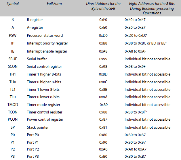
8051 has the SFRs (Figure 3.1). SFRs are listed in Table 3.2, Column 1. The SFRs are at directly addressable space. Each SFR can be addressed by an address of 8-bits. Table 3.2 also specifies the addresses of the bytes at the SFRs. Each bit can be addressed in specific SFRs and bit can be cleared to 0 or set to 1 or moved to another bit address. The addresses of these bits are used in Boolean processing logical operation on the bits. Table 3.2 also shows the bit addresses for these operations. Specific SFRs can only be addressed for the byte in them not individual bits.
Example 3.1
- What are the addresses of bits P1.6 and P1.7 in Boolean processing instructions of 8051?
0x96 and 0x97 are the addresses of bits P1.6 and P1.7.
- What are the addresses of bits b6 and b7 in TMOD of 8051?
Bits b6 and b7 in TMOD cannot be accessed or set by Boolean processing instructions of 8051. We have to use the address 0x89 and do byte operations to set the bits b6 and b7.
Example 3.2
What are the Special Function Registers and bits used by timers in 8051? What are their addresses?
TH1, TL1, TH0, TL0, TMOD and higher four bits b4, b5, b6 and b7 of TCON of bits are used by timers. (Section 3.5.1) Addresses for the bytes at 8051 for TH1, TL1, TH0, TL0, TMOD are 0x8D, 0x8B, 0x8C, 0x8A and 0x89, respectively. Addresses for the higher four bits TCON.4, TCON.5, TCON.6 and TCON.7 are 0x8C, 0x8D, 0x8E and 0x8F, respectively.
3.1.3 PSW Register Bits And Flags
A flag is a bit that may be set or reset after an ALU operation. A flag or a set of flags can reflect status of the processor. A bit is also set or reset after a bit-set, bit-reset, or bit-complement operation or a bittransfer operation. The PSW register byte, being an SFR is directly addressable. PSW individual bits are directly addressable also.The bit addresses (byte addresses) in column 3 of row 3 in Table 3.2 are used.
Table 3.3 specifies the individual bit addresses of PSW bits. These addresses are used in a Boolean-processing logical-operation on the bits. Note that there is a convention that the right most least significant bit is denoted by b0. Therefore, the leftmost maximum significance bit is denoted by b7. Further, b7 of PSW is denoted by PSW.7 or PSW^7 and b0 of PSW by PSW.0 or PSW^7. Similar convention will be henceforth used for referring to the bits of PSW and other SFRs.
Example 3.3
- How can we select register bank 1 using Boolean-processing instructions of 8051?
RS1-RS0 are loaded with 0 and 1 using their bit addresses 0xD4 and 0xD3, respectively, using Boolean-processing instructions.
- How is the PSW byte addressed in 8051?
PSW byte is addressed by 0xD0 in instructions for the byte operations.
- What is the bit address of C in 8051?
Bit b7 in PSW is C and its address is 0xD7.
Table 3.3 Processor Status Word Register Bits and Flags

Note. Z flag indicates the result of an ALU operation on A, whether A has all bits cleared and equals 0s or not. 80x86 and 8085 processors have Z flag. Z flag is of importance in a program that has loops and other conditional branch or call instructions. However, there is no Z flag. This is because of the fact that PSW design limits it to only 8 bits. It is providing for two-user flags and two register bank select in 8051. (A bank is a set of 8 registers). Internally (not to programmer), the Z flag is accessible to the condition test and branch logic circuit and instruction like JZ. The latter uses this internal Z.
a Bit addresses are for the Boolean-processing operations.
b C is also used in Boolean-processing operations for loading a bit from an address or storing a bit to an address.
Example 3.4
When does the auxiliary carry sets? Give an example when the carry is not set but auxiliary carry sets.
Auxiliary carry sets when after addition the result of adding lower nibble (4-bits) exceeds 0xF. An example is as follows: When 0x1B and 0x35 are added, the result of lower nibble addition B + 5 exceeds 0xF, it is 0x0. The final result is 0x50 by adding both nibbles. C is not set to 1 and auxiliary carry is set to 1 on addition of 0x1B and 0x35.
3.1.4 The 8052/8032 Family
The 8032 and 8052 are similar in their architecture. 8032 does not have an internal program memory. Therefore, the Ports P0 and P2 are used for interfacing to external memory. All the program memory needed is to be interfaced externally. 8052 has internal program memory. 4 kB of internal program memory is present in Classic 8052.
Additional RAM
The RAM is 256 B from 0x00 to 0xFF in 8052. The additional RAM cannot be directly addressed. RAM address space between 0x80 to 0xFF of 128 B out of 256 B RAM is only indirectly addressable. This is because the SFRs are also having addresses between 0x80 and 0xFF and they are distinct from the RAM and are directly addressable.
Additional Timer
8052 family microcontrollers have an additional timer, T2. Pin is. P1.1 is used for T2 to capture the timer counts in a register. It is also used for a triggering-input for reload of the counts in timer from a register. Pin P1.0 is for timer T2 input (−ve edge) for counting the external events in T2. Additional SFRs in 8052 family are listed in Table 3.4.
Table 3.4 Additional Special Function Registers in 8052

There is an additional interrupt INT2. P1.1, another alternative use is as an additional external interrupt pin, INT2.
3.1.5 ATMEL 89C51
89C51 is a flash memory version of microcontroller and C stands for CMOS version. CMOS version dissipates less power. Atmel offers number of 89C51 versions—the 89C51-20PC, 89C51-16PC and 89C51-12PC. They are 20 MHz, 16 MHz and 12 MHz versions, respectively. PC means plastic packaging and commercial 0 to 70°C versions. Details of all AT89V51 family versions are at the www.atmel.com. The features in a few of them are given in Table 3.5.
Table 3.5 ATMEL 89C51 Versions
| Chip | Operation Voltage and Packaging | Features |
|---|---|---|
AT89C2051 |
2.7-Volt, 20-Pin Package |
80C31 with 2kB flasha |
AT89C4051 |
3 Volt, 20-Pin Package |
80C31 with 4 kB flasha |
AT89C51RC |
|
80C51 with 32 kB flasha. |
AT89C55WD |
|
80C32 with 20kB flasha. |
AT89C51-20PC |
|
20 MHz |
AT89C51AC2 |
|
80C51 with 32 kB flash, 2kB EEPROM and 10-bit A/D converter |
AT89C51AC3 |
|
8-bit microcontroller with A/D converter and 64-Kbyte flash. 2-Kbyte RAM, 2-kB EEPROM, SPI. Power fail detect, no need of external brown out protectionb |
a Requires external brown out protection. Brown out protection built-in.
b Brown out protection means during low voltage, a microcontroller should not wrongly interpret the code at the SFRs, IO registers, Flash/EEPROM. The corruption of bits during power-on or power-off. On-chip memory is protected from low voltage situations by the brown out protect circuit.
3.2 MICROCONTROLLER 8051 PINS
Figure 3.2 shows forty pin signals in an 8051 series microcontroller. It shows the I/O pins − P0.0 to P0.7, P1.0 to P1.7, P2.0 to P2.7 and P3.0 to P3.7. It also shows the other remaining eight pins, VDD, VSS, XTAL1 and XTAL2, ![]() , ALE,
, ALE, ![]() and
and ![]() . Table 3.6 lists these and gives the use(s) of each pin.
. Table 3.6 lists these and gives the use(s) of each pin.
What are alternative uses of P1.6 and P1.7 in certain 8051 versions?
P1.6 and P1.7 are used for the serial clock and data line for the I2C serial bus in P83C528 member of 8252 family. I2C serial bus is a bus used for the inter integrated circuit communication. It was first introduced by Philips and is now a standard bus for many applications and systems and in used in several versions of 8051.

Figure 3.2 Pins/signals in an 8051 Family Microcontroller

Note: It is conventional that .n represents the nth pin or nth bit. PSW.5 represents the fifth bit of PSW and P2.3 represents the third pin of P2 starting from the 0th pin. Port 1 bits are also used in 8051 for extended features in certain versions.
Example 3.6
What are the alternative uses of P1.0 and P1.1 in 8052?
8052 families use the pins P1.0 and 1.1 for timer T2 for (i) input (−ve edge) in T2 on the external event input and (ii) T2 timer counts capture or reload triggering input, respectively. P1.1 another alternative use is as an additional external interrupt pin, ![]() .
.
3.3 8051 PORTS
(1) Single-chip mode: Single-chip mode is a mode in which all the software and data internally embed into the microcontroller and external memory chips are not used. This is feasible provided the finally tested, optimized code size is equal or less than available internal memory space, and the internal RAM suffices for all the operations.
Table 3.7 gives this mode feature and SFRs for the respective port latches. Quasi bi-directional means can be used for input to LSTTL chip for just a few clock cycles without using a pull-up to supply pins.
Table 3.7 Ports in Single-chip Mode Operations

Example 3.7
An 8051 variant AT89LV52 has 8 kB. What are the addresses in the program codes available in singlechip mode operation?
Addresses 0x0000 to 01FFF will be available in single-chip mode operation. ![]() is set to 1 to inactivate external addresses 0x0000 to 01FFF inaccessible.
is set to 1 to inactivate external addresses 0x0000 to 01FFF inaccessible.
(2) Expanded multiplexed mode: All the software (and data) embed either internally or externally or only externally in the system and the external devices (circuits) interface with the microcontroller in this mode. Therefore, the external memory chips interface with the microcontroller. This is when the code size is more than the available internal memory space, and the internal RAM is not sufficient for all the operations. Table 3.8 gives the uses during operations in this mode.
Table 3.8 Ports Alternate Use in Expanded Mode of Operations
| Port | Name | Use |
|---|---|---|
P0 |
Lower address/data bus |
AD0-AD7 bus, which uses the PCL when program memory access and the DPL when data memory access occurs. Internal pull ups for two clock cycles and 8 LSTTLs. |
P2 |
Higher order address bus |
A8-A15 bus using PCH when program memory access and DPH When data memory access occurs. Internal pull ups for two clock cycles and 8 LSTTLs. |
P1 |
Timer or serial devices control bus in 8052 family and 8051 variants. |
Port pin P1.1 for T2 event counter input. P1.2 for either timer capture/reload or INT2 pin. P1.6 and P1.7 for external serial I2C bus clock and data in/out, respectively in P83C528. |
P3 |
Port P3 |
RxD at P3.0 and TxD at P3.1, when the SI operation enabled; |
Figure 3.3 (a) and (b) show the port pins for outputs and inputs. Figures 3.4 (a) to (d) show the port inputs and output pins in expended mode.

Figure 3.3 (a) Output Port Bits Each with a D-latch and (b) Input Port Bits Each with a D-latch (Eout when active enables output. Ein when active enables input. CL clock latch input when active enables Q output on a D-latch.)

Figure 3.4 (a) P0 in Expanded Mode; (b) P2 in Expanded Mode; (c) P3 in Expanded Mode and (d) P1 in Expanded Mode
3.4 INTERNAL AND EXTERNAL MEMORY
(1) Internal program memory: Figure 3.5 shows a layout of the internal code (program codes and constants as per Table 2.2) memory addresses in the classic 8051 architecture. When the ![]() is 1 at the instance of RESET, It means external not enabled. The PC starts from 0x0000. Processor accesses the internal addresses from the memory. Memory addresses are between 0x0000 and 0x1FFF for 4kB (two code banks) of codes. In certain versions, it is 8 kB (4 code banks) and in a certain version, 16 kB (8 code banks). Code memory area of 64 kB can be considered as consisting of 32 code-banks, each of 2 kB in the classical 8051.
is 1 at the instance of RESET, It means external not enabled. The PC starts from 0x0000. Processor accesses the internal addresses from the memory. Memory addresses are between 0x0000 and 0x1FFF for 4kB (two code banks) of codes. In certain versions, it is 8 kB (4 code banks) and in a certain version, 16 kB (8 code banks). Code memory area of 64 kB can be considered as consisting of 32 code-banks, each of 2 kB in the classical 8051.
(2) Internal data memory (internal RAM) IDATA data bytes, registers and bits (in classic 8051): Figures 3.6(a) and (b) show a layout of the DATA and IDATA internal data memory in the classic 8051 architecture. DATA is abbreviation for direct or indirect access RAM bytes. I-DATA is the abbreviation for the indirectly addressed data bytes and bits for indirectly addressed bytes in the internal RAM only. Figure 3.6(a) shows the layout of the DATA (internal RAM 0x00–0x7F) and SFR direct addressable space 0x80–0xFF in the classic 8051 family versions. IDATA and DATA address space are same in internal RAM between 0x00–0x7F.

Figure 3.5 CODE and CONSTANTS [Internal Program Codes and Constants] in 4kB Memory Area in Classic 8051
SFRs are between 0x80 and 0xFF. Several SFR bytes, for example, P0, P1, P2 and P3 are also used for the bit operations with Boolean processor and bit transfers. The SFR space between 0x80 and 0xFF is accessible by the address, which is directly pointed by address in an instruction. (Table 3.2)
- The RAM IDATA/DATA is between 0x00 and 0x7F. The IDATA/ DATA RAM between 0x00 and 0x7F has 128 bytes that is accessible by the address indirectly pointed by R0 and R1 in an instruction or directly pointed address in an instruction. 8052 has 256 B IDATA.
- The RAM DATA between 0x00 and 0x1F out of the 0x00 and 0x7F has 32 bytes, which define four register sets (called banks in 8051 terminology). Each bank (bank 0, bank 1, bank 2, and bank 3) is selected by first assigning the RS0 and RS1 bits b3 and b4 in the PSW (Table 3.3). Therefore, during an instruction only three bits can specify the addresses register (RAM) in place of the eight bits needed otherwise. These 32 bytes are not used for the bit operations with Boolean processor and bit transfers.
- RAM between 0x20 and 0x2F out of the 0x00 and 0x7F has 16 bytes, which also define 128 bits with bit-addresses 0x00 to 0xFF. A bit address is used in bit operations with Boolean processor and for bit transfers.
- RAM between 0x30 and 0x7F out of the 0x00 and 0x7F has 80 bytes, which is only accessible by the address of the byte and is not used in bit operations with Boolean processor and bit transfers.
Figure 3.6(b) shows a layout of the IDATA in internal RAM in the classic 8051 and 8052 versions. The RAM between 0x80 and 0xFF out of the 0x00 and 0xFF has additional 128 bytes in 8052. This is only accessible by the address indirectly pointed (called indirect or base addressing mode) in an instruction. It is not used in bit operations with Boolean processor and bit transfers.
(3) External program memory: Figure 3.7 shows a layout of the external code (program code CODE and CONSTANTS) memory addresses in the classic 8051 architecture. Same is for 8052.


Figure 3.7 Code Memory (External) for CODE and CONSTANTS
- When the
 is 0 at RESET, the PC ( program counter) starts from 0x0000 and accesses the external addresses from the memory. Memory addresses are between 0x0000 and 0xFFFF (Code-Bank 0 to 31) for 64 kB of codes.
 - When the is 1 at RESET, the PC starts from 0x0000 for code-banks 0 and 1. Instructions are accessed from the internal addresses and the PC=0x1000 onwards from the external addresses. This is for the case of 4 kB internal program memory.
External memory addresses are accessed between 0x0000 and 0xFFFF for 64 kB of codes and constants (Table 2.2) when ![]() is 0 and between 0x1000 and 0xFFFF for 60 kB (code-banks 2 to 31) of external codes when
is 0 and between 0x1000 and 0xFFFF for 60 kB (code-banks 2 to 31) of external codes when ![]() is 1 during the RESET interval.
is 1 during the RESET interval.
(4) External data memory X-Data (RAM): Figure 3.8 shows a layout of the external data (abbreviated as X-DATA) memory addresses in the classic 8051 architecture. It can be accessed through the indirect addressing mode used (for example, when the DPTR is used) in an instruction.
Example 3.8
An 8051 variant AT89LV52 has 8 kB program memory. What are the internal and external addresses in the program codes accessible in expanded chip mode operation?
Internal addresses 0x0000 to 01FFF will be accessible and external memory chip addresses 0x2000 to 0FFFF are accessible in the expanded mode operation when ![]() is not active and equals 1 at the reset. Internal addresses 0x0000 to 01FFF will not be accessible and external memory chip addresses 0x0000 to 0FFFF are accessible in expanded mode operation when
is not active and equals 1 at the reset. Internal addresses 0x0000 to 01FFF will not be accessible and external memory chip addresses 0x0000 to 0FFFF are accessible in expanded mode operation when ![]() is active and equals 0 at the reset.
is active and equals 0 at the reset.
(5) Interfacing of external memories in Intel 8051: External memories are interfaced using four control signals (![]() , ALE,
, ALE, ![]() and
and ![]() ) and AD-AD7 bus at P0 and A8-A15 at P2. Figure 3.9(a) shows the circuit, the interfacing circuit and Figure 3.9(b) shows the clock states, when the program memory is read and data memory is written. (Section 3.4.(6)). Interfacing signals are as follows:
) and AD-AD7 bus at P0 and A8-A15 at P2. Figure 3.9(a) shows the circuit, the interfacing circuit and Figure 3.9(b) shows the clock states, when the program memory is read and data memory is written. (Section 3.4.(6)). Interfacing signals are as follows:
- ALE signal =1 during a clock state and using it a latch circuit separates the A0-A7 bus for the program and X-data memories.
 signal when 0, uses the program memory code bank 2 to 31 for the code reading operation. Uses Bank 0 and Bank 1 also when is 0 during the RESET of the microcontroller.
 when 0, uses data memory for the X-data reading operation in the new cycle.

Figure 3.8 Memory for X-data Area in Classic 8051
 when 0, uses data memory for the X-data-write operation in the new cycle.

When ![]() and
and ![]() are short-circuited, the program memory and data memory spaces overlap. We can place both codes and data in the unified space.
are short-circuited, the program memory and data memory spaces overlap. We can place both codes and data in the unified space.
Example 3.9
How will we interface two 16 kB each program memory chips PM1 and PM2 at external addresses 0x0000 to 0x3FFF and 0x4000 to 0x7FFF, respectively?
When number of bytes = 0x1000, it means 212 = 4096 = 4 kB in memory. Each PM chip has total number of bytes = 16 kB. It 0x4000 means it has 214 = 4 × 4096 = 0100 0000 0000 0000b addresses of memory. Each needs 14 address lines for access to 214 = = 0x4000 Byte. Each program memory chip should have address input lines from A0 to A13 and the address bits change from 00 0000 0000 0000b to 11 1111 1111 1111b.
Eight A0 to A7 bus signals are at the 8-pins of P0. Six A8 to A13 lines are P2.0, P2.1, P2.2, P2.3, P2.4 and P2.5.Therefore, A0 to A13 address lines using 8 pins of P0 and 6 pins of P2 are interfaced to A0 to A13 lines in PM1 and A0 to A13 lines in PM2.
A14 and A15 signals are at P2.6 and P2.7, respectively. P2.6 and P2.7 are interfaced to input of a decoder. The decoder output ![]() will be active when P2.7-P2.6 are 00. Thus, PM1 chip select
will be active when P2.7-P2.6 are 00. Thus, PM1 chip select ![]() pin is interfaced to Y0. The decoder output Y1 will be active when P2.7-P2.6 are 01. Thus, PM2 chip select CS pin is interfaced to Y1.
pin is interfaced to Y0. The decoder output Y1 will be active when P2.7-P2.6 are 01. Thus, PM2 chip select CS pin is interfaced to Y1.
Control signal ![]() pin in 8051 is interfaced to Read pin in PM1 and Read Pin in PM2. Figure 3.10(a) shows the interfacing circuit for the program memory chips.
pin in 8051 is interfaced to Read pin in PM1 and Read Pin in PM2. Figure 3.10(a) shows the interfacing circuit for the program memory chips.
Example 3.10
How will we interface two 32 kB each data memory chips DM1 and DM2 at external addresses 0x0000 to 0x7FFF and 0x8000 to 0xFFFF, respectively?
When number of bytes = 0x1000, it means 212 = 4096 = 4 kB of memory. Each DM chip has total number of bytes = 32 kB. It 0x8000 means it has 215 = 8 × 4096 = 1000 0000 0000 0000b addresses of memory. Each needs 15 address lines for access to 215 = 0x8000 Byte. Each data memory chip should have address input lines from A0 to A14 and the address bit changes from 000 0000 0000 0000b to 111 1111 1111 1111b. Eight A0 to A7 signals are at the 8-pins of P0. Seven A8 to A14 lines are P2.0, P2.1, P2.2, P2.3, P2.4, P2.5 and P2.6.Therefore, A0 to A14 address lines using 8 pins of P0 and 7 pins of P2 are interfaced to A0 to A14 lines in DM1 and A0 to A13 lines in DM2. A14 and A15 signals are at P2.6 and P2.7, respectively. P2.6 and P2.7 are interfaced to input of a decoder. The decoder output Y0′ will be active when P2.7 is 0. Thus, DM1 chip select CS pin is interfaced to Y0′. The decoder output Y1′ will be active when P2.7 are 1. Thus, DM2 chip select CS pin is interfaced to Y1′. Control signal ![]() at P3.7 pin in 8051 is interfaced to
at P3.7 pin in 8051 is interfaced to ![]() pin in DM1 and RD Pin in DM2. Figure 3.10(b) shows the interfacing circuit.
pin in DM1 and RD Pin in DM2. Figure 3.10(b) shows the interfacing circuit.
(6) Timing diagrams when accessing the external memories in Intel 8051: For an instruction cycle there are twelve clock states, spread over two cycles—S1 to S6. The twelve clock states are marked S1 to S6 and again S1 to S6 in next instruction cycle. Two set of 6 states are thus for a period of 12 times the oscillator clock period. One clock period is equal to the reciprocal of the XTAL frequency.
Figure 3.9(b) shows the clock states and the timing diagram to reflect the sequence of bus operations.
- During the period between the middle of two clock states, S1 and S2, period first ALE signal (=1) the A0–A7 bus seperates using latch.
- During a period between the nearly end of clock state, S2 and middle of S4, signal when 0, microcontroller reads the program memory code (instructions’s byte).
- Assume that instruction requires to read a byte from X-DATA. It will be in next set of six states. During the three-clock period between the beginning of S1 and end of S3, the when 0 and , data memory is read. The new S1 and S3 are after the first set of six clock states S1–S6.
- Assume that instruction requires to write a byte to X-DATA. It will be in next set of 6 states. During the three-clock period, between the beginning of S1 and end of S3, when 0, uses data memory for the write. The new S1 and S3 are after the first cycle of six clock states, S1–S6.
- Just before the ALE is 1 and just after ALE becoming 0, the P0 has the bits of PCL buffer. Just before the ALE is 1 at S1 and up to just before the next time, another ALE activation at S4, the P2 has the PCH buffer bits. Another activation of ALE occurs when another byte in the instruction is also to be read.
- An instruction is read in between the period of = 0 and between the middle of S3 to just before the start of next ALE at S4.
- Just after beginning of S4, the DPL is out for one state period (middle of S4 to middle of S5) before the ALE = 1 at S4. During the write, the data is at P0 after S5 up to just after the end of S3 in next S1, S2, and S3 when or is low.
- Just after the beginning of S4, the DPH is out for periods (middle of S4 to just after the end of S3) in next S1, S2 and S3 when or is low.

3.5 COUNTERS AND TIMERS
A counter, given the count inputs at regular intervals (called clock inputs), also functions as a timer. Figures 3.11(a) and (b) show the counter and timer circuits block diagram.
Figure 3.12(a) and (b) show the pre-loading counter and timer circuit block diagrams. Figure 3.12(c) and (d) show the auto-loading counter and timer circuit block diagrams. Functions of counter and timer can be understood by following examples.
Example of Timer/Counter Overflow Interrupt
Example 3.11
Consider a counter variable, x, reset occurs when x = 0000 0000b (=0x00). If it is given the count inputs from a source, it will increment on each input until its value = 1111 1111b (0xFF). After the next input, it will overflow and then the x becomes 0x00 once again. Overflow indication may be given by an output, called overflow interrupt output (timer timeout). If the counter is given inputs at successive intervals after each 1 μs, it will interrupt (timeout) after (0xFF + 1) = 256 times the interval, that is, it means in 256 μs.
Example of 8-bit Timer/Timer Operations with Preloaded Counts
Example 3.12
Suppose the counter is pre-loaded with the count = 1000 1000 (= 0x88), if it is given the successive interval 1 μs pulses, it will timeout in (0xFF − 0x88 + 1) = 120 μs. If the successive interval is 8 μs and the pre-loaded value in the counter is 0xF0H, it will timeout after (0xFF − 0xF0H + 1) × 8 μs = 128 μs.
Example of 8-bit and 16-bit Timer Operations with Preloaded Counts
Example 3.13
What should be the pre-loaded value in a counter of 16 bits if it is given inputs at 8 μs interval and timeout interrupt is required after 4.096 ms?
The maximum count variable x for 16-bit counter is 0xFFFF (= 65535) and minimum is 0. Let the loaded value be x0. The timeout interrupt will occur after (65535 − x0 + 1) intervals = (65536 − x0) × 8 μs. This should be equal to 4096 μs.
(65536 − x0) × 8 = 4096. Therefore, (65536 − x0) = 512. Therefore, x0 = (65024) = 1111 1110 0000 0000b.
Example of a 16-bit Counter Operation with Pre-load


Figure 3.12 (a) Counter Circuit Block Diagram with Pre-load; (b) Timer Circuit Block Diagram with Pre-load; (c) Counter Circuit Block Diagram With Auto-load After Each Overflow and (d) Timer Circuit Block Diagram with Auto-load After Each Overflow
Example 3.14
What should be the pre-loaded value in a counter of 16 bits, if it is given inputs from an external pin to count 512 events and after 512 events it should give required overflow interrupt ?
Let the loaded value be x1. The overflow interrupt will occur after (65536 − x1) = 512. This equals to 65024 = 1111 1110 0000 0000b.
Example of a 16-bit Counter Values After the New Count inputs
Example 3.15
A counter shows counts reading 1111 1110 0000 0000b and during time t0 that is given 256 inputs from an external pin to count the events. What are the counts after t0? What are the counts after next 256 inputs? What are the counts after another 256 inputs again?
- After t0 the counts will be 1111 1110 0000 0000b + 0000 0001 0000 0000b = 1111 1111 0000 0000b. There will be no overflow.
- After another 256 inputs the counts will be 1111 1111 0000 0000b + 0000 0001 0000 0000b = 0000 0001 0000 0000b. There will be overflow now.
- After another 256 inputs the counts will be 0000 0000 0000 0000b + 0000 0001 0000 0000b = 0000 0001 0000 0000b. There will be no overflow.
3.5.1 Programmable Timers in the Intel 8051 Family
Figures 3.13(a) and (b) show the modes of timers T0 and T1. Figure 3.13(c) shows the function of T2, additional timer of 8052. Figure 3.13(d) shows watchdog timer T3 function method in certain 8051 variant.
Table 3.2 showed that:
- There are two timers, T0 and T1.
- Two SFRs, which correspond to timer 0-count variable(s), are TH0 and TL0.
- Two SFRs, which correspond to timer 0-count variable(s), are TH1 and TL1.
- An SFR, which controls the timer T0 and T1 functions, is TCON.
- An SFR, which defined modes of the timer T0 and T1 functions, is TMOD.
Programming a timer means programming the TCON and TMOD bits and loading the appropriate count variable as per the intervals of the clock inputs to the timer/counter.
(1) Timer-0 and Timer-1: Tables 3.9 to 3.11 give the functions of SFRs related to the timers and meaning of bits in each SFR. Table 3.11 gives the meanings of modes 0, 1, 2 and 3 in the Timers T0 and T1.
Table 3.9 Special Function Registers for the Timers
| SFR Symbol | Direct Address | Explanation of the Function |
|---|---|---|
TH1 |
0x8D |
Saving and counting value for the Timer 1 higher 8-bits. |
TH0 |
0x8C |
Saving and counting value for the Timer 0 higher 8-bits. |
TL1 |
0x8B |
Saving and counting value for the Timer 1 lower 8-bits. |
TL0 |
0x8A |
Saving and counting value for the Timer 0 lower 8-bits. |
TMOD |
0x89 |
Define (program) the counting modes for the T0 and T1. |
TCON |
0x88a |
Timer device control bits. It is either by transfer of the control byte at the address 0x88 or by transferring the control bits one by one using bit-addresses between 0x88H to 0x8F. |
a TCON individual bit is also programmable by the bit addresses of the 8 bits during Boolean processing or bit-transfer instruction.

Figure 3.13 (a) Timer 0 Functions in 8051; (b) Timer 1 Functions in 8051; (c) Functions of Additional Timer at 8052 and (d) Using the WDT Timer (T3) Function
Table 3.10 Meaning of Each bit of TMOD Register (Direct Address = 0x89)

a A control bit for timer start in TCON (Table 3.11, Rows 2 and 4).
b In order to count a −ve edge at external input, it must be 1. Logic 1 must be at least for period T. It should also be held 0 at least for period T. In other words, during the count of external input −ve edges, a count could be missed if a pulse is for a period shorter than 2T. Here, T is the machine cycle period (1μs for 12 MHz crystal oscillator).
Table 3.11 Meaning of Each Bit of TCON Register (Direct Address = 0x88 for the Byte and Bit Addresses of TCON are From 0x88 to 0x8F)

a Timer/counter increment will occur when at input a -ve edge occurs, provided the timer/counter is enabled by TR bit.
b Not related to the T1 or T0.
Table 3.12 Meaning of Mode 0, 1, 2 and 3 of T1 and T0 Timers

a The timer-1 in mode 0 overflow in mode 0 occurs when all the 5 bits in TL1 and 8 bits in TH1 undergo transition from 11111 and 11111111 to 00000 and 00000000, respectively.
b The timer-0 in mode 0 overflow in mode 0 occurs when all the 5 bits in TL0 and 8 bits in TH0 undergo transition from 11111 and 11111111 to 00000 and 00000000, respectively.
c When timer 0 runs in mode 3, the timer 1 when programmed in mode 0 or 1 or 2, cannot set timer-1 interrupt request flag TF1 on overflow, and cannot generate interrupt due to overflow. This is because TF1 is now assigned to TH0 timer. However, Timer 1 overflow can still be used for the serial port bit transmission.
The details of using timer/counter will be discussed in Chapter 6. The following examples explain the application of mode 2 of timer T0.
Example of T1 Mode 0
Example 3.16
How will you program timer T1 to interrupt after 8 ms using mode 0 and oscillator of 12 MHz with 8051?
Internal oscillator is 12 MHz. Input clock interval is therefore 12/f = 1 μs. Mode 0 has pre-scaling factor of 32 for TH1 and timer functions as 13-bit timer. T1 overflows after 213 inputs of clock. Overflow interrupt after 8 ms means overflow after each 250 × 32 μs. TL1 in mode 0 overflows after 32 inputs and send input clock count to TH1 after 32 clock inputs. Therefore, TH1 should be loaded with value (256–250)=0x06 and TL1with value 0x00.
- First step is to program T1 in mode 0. This is because in the mode 0, T1 operates as an 13-bit timer/counter TMOD.4 and TMOD.5 are set to both 0 and 0.
- Second step is reset TMOD.6 to 0 to use the T1 as timer not as counter.
- Third step is reset TMOD.7 to 0 to disable external control for run and run the timer T1 using TR1 alone.
- Fourth step is TL1 8-bit preloaded counts x00.
- Fifth step is TH1 8-bit preloaded counts x06.
- Sixth and final step is set TCON.6 = 1 to run the timer 1.
Using address of TMOD for the byte, we set upper 4 bits of TMOD = 0000. Using address of TL1 for the byte, we set 8 bits of TL1 = 0000 0000. Using address of TH1 for the byte, we set 8 bits of TH1 = 0 0110. Using address of TCON.6 bit, we set the bit at 1. Timer T1 is programmed to interrupt after 8 ms from the sixth step.
After 8 ms TF1 bit in TCON.7 sets to 1.
Example of T0 Mode 1
Example 3.17
How will you program timer T0 to interrupt after 16 ms using mode 1 and oscillator of 12 MHz with 8051?
Internal oscillator is 12 MHz. Input clock interval is therefore 12/f = 1 μs. Mode 0 can timeout maximum in 213 = 8.192 ms for 12 MHz with 8051. Hence, mode 0 cannot be used for 16 ms timeout requirement. Mode 2 and 3 are the 8-bit timer modes. Hence, mode 2 or 3 cannot be used for 16 ms timeout requirement.
Mode 1 has pre-scaling factor of 1 for TL0 and of 256 for TH0 timer. The TH0-TL0 combination functions as 16-bit timer. T0 overflows after 216 inputs of clock. Overflow interrupt after 16 ms means overflow after each 62 × 250 + 128 μs.
TL0 in mode 1 if initial value loaded = 0x80 overflows after 128 inputs in first stage then send input clock count to TH0, and later on to TH0 after every 256 clock inputs to TL0. Therefore, TH0 should be loaded at the start with value (256 − 62) = 194 = 0xC2 and TL0 with value 0x80.
- First step is to program T0 in mode 1. This is because in mode 1, T0 operates as an 16-bit timer/ counter. TMOD.1 and TMOD.0 are set to 0 and 1.
- Second step is reset TMOD.2 to 0 to use the timer/counter T0 as timer.
- Third step is reset TMOD.3 to 0 to disable external control for run and run the timer T1 using TR1 alone.
- Fourth step is TL0 8-bit preloaded with counts 0x80.
- Fifth step is TH0 8-bit preloaded with counts 0xC2.
- Sixth and final step is set TCON.4 = 1 to run the timer 0.
Using address of TMOD for the byte, we set lower 4 bits of TMOD = 0001.
Using address of TL0 for the byte, we set 8 bits of TL0 = 1000 0000. Using address of TH0 for the byte, we set 8 bits of TH0 = 1100 0010. Using address of TCON.4 bit, we set the bit at 1. Timer T0 is programmed to interrupt after 16 ms from the sixth step.
After 16 ms TF0 bit in TCON.5 sets to 1.
Example of T0 Mode 2
Example 3.18
How will you program timer T0 to interrupt after every 20 μs?
Consider the auto-reload mode. If counter TL0 is loaded (256 − 20) = 0xFF + 1 − 0x14 = 0xEC, then after twenty inputs of clock input it will timeout. If T0 is programmed in auto reload mode and XTAL frequency f = 12 MHz, the inter clock input will be after each 12/f = 1 μs. There will be interrupts after each timeout after every 20 μs if it is auto-loaded 0xEC.
- First step is to program T0 in mode 2. This is because in the mode 2 the T0 operates as an 8-bit timer/counter TL0 with 8-bit pre-loaded counts at TH0 and auto reloading from TH0 after each timeout overflow of TL0 (pre-scaling none [=1]). TMOD.1 and TMOD.0 are the bits M1-M0 for timer T0 = 10.
- Second step is reset TMOD.2 to 0 to use the timer/counter as timer.
- Third step is reset TMOD.3 to 0 to run the timer using TR0 alone.
- Fourth step is to load TH0 with 0xEC.
- Fifth and final step is set TCON.4 = 1 to run the timer 0.
Using address of TMOD for the byte, we set lower 4 bits of TMDO = 0010. Using address of TH0 for the byte, we set 8 bits of TH0 = 1110 1100. Using address of TCON.4 bit, we set the bit at 1. Timer T0 is programmed to interrupt after every 20 μs. After every 20 μs, TF0 bit in TCON.5 sets to 1.
Example 3.19
A How will you program timer T0 to interrupt after 127.8 μs and 19.8 μs using mode 3? Assume oscillator of 20 MHz is used with 8051 version AT89C51-20.
The internal oscillator is 20 MHz. Input clock interval is therefore 12/f = 0.6 μs. Mode 3 8-bit timers can timeout maximum in 28 = 256 × 0.6 μs = 153.6 μs for 20 MHz with 8051 version. Mode 3 are the 8-bit timer modes. Hence, mode 2 or 3 cannot be used for 16 ms timeout requirement.
Mode 3 has pre-scaling factor of 1 for TL0 and same 1 for TH0 timer. The TH0 and TL0 function as two 8-bit timers. TL0 overflows after (28 − x0) inputs of clock if loaded with counts x0. TH0 overflows after (28 − x1) inputs of clock if loaded with counts x1. Overflow interrupt after 127.8 μs and 19.8 μs means overflow after each 213 × 0.6 μs and 33 × 0.6 × 33 μs.
TL0 in mode 3 if initial value loaded = 256 − 213 = 43 = 0x2B overflows after 213 inputs. TH0 in mode 3 if initial value loaded = 256 − 33 = =223 = 208 + 15 = 0xDF overflows after 33 inputs. TH0 should be loaded at the start with value 0x2B and TL0 with value 0xDF.
- First step is to program T0 in mode 3. This is because in the mode 3 the T1 stops and T0 operates as two 8-bit timer/counters. TMOD.5, TMOD.4, TMOD.1 and TMOD.0 are set to 1 each.
- Second step is reset the TMOD.2 and TMOD.6 to 0 and 0 to use the timer/counter T0 as timer.
- Third step is reset the TMOD.7 and TMOD.3 to 0 and 0 to disable external control for run and run the timer TH0 and TL0 using TR1 and TR0 alone.
- Fourth step is TL0 8-bit preloaded with counts 0xDF.
- Fifth step is TH0 8-bit preloaded with counts 0x2B.
- Sixth and final step is set TCON.6 and TCON.4 set to 1 and 1 to run the TH0 and TL0.
Using address of TMOD for the byte, we set 8 bits of TMOD = 00110011. Using address of TL0 for the byte, we set 8 bits of TL0 = 1101 1111.Using address of TH0 for the byte, we set 8 bits of TH1 = 1100 0010. Using addresses of TCON.6 and TCON.4 bits, we set the bits = 1 and 1. Timer TH0 and TL0 are programmed to interrupt after 127.8 μs and 19.8 μs from the sixth step. After 127.8 μs and 19.8 μs TF1 and TF0 bits in TCON.7 and TCON.5 sets to 1.
3.5.2 8052 Additional Timer T2
The uses of Timer 2 (Fig. 3.13(c))as a timer are as follows:
- 16-bit auto-reload timer.
- 16-bit input capture on an input negative edge.
- Baud rate generator for receiving and transmitting at identical rates.
- Receive clock set for a serial port.
- Transmit clock set for at a serial port.
T2 can be used as counter in following ways:
- 16-bit auto-reload counter.
- 16-bit input capture of the timer 2 counts on the input negative edges.
Table 3.13 gives the SFRs related to timer T2. Table 3.14 gives meaning of the bits at each T2CON SFR bit address.
Table 3.13 Special Function Registers for the Timer 2
| SFR Symbol | Direct Address | Explanation of the Function |
|---|---|---|
TH2 |
0xCD |
Saving and counting value for the timer 2 higher 8-bits. |
TL2 |
0xCC |
Saving and counting value for the timer 2 lower 8-bits. |
RCAP2H |
0xCB |
Saving the re-loadable or captured value higher 8-bits. |
RCAP2L |
0xCA |
Saving the re-loadable or captured value lower 8-bits. |
T2CON |
0xC8a |
Programming the timer 2 device control bits either by transfer the control byte at the address 0xC8 or by transferring the control bits one by one using bit-addresses between 0xC8H to 0xCF (Table 3.14). |
a T2CON Individual bit is also programmable by the bit addresses of the 8 bits during Boolean processing or bit transfer instruction (Table 3.14).
Table 3.14 Meaning of Each Bit of T2CON Register at Direct Address 0xC8

a TF2 is to be reset to 0 again by writing bit 0 using clear T2CON.7 instruction. TF2 does not set automatically. When either RCLK = 1 or TCLK = 1, the timer 2 is dedicated to serial port and is used to program times lot interval for a serial bit.
b Control bit for timer 2 start.
c In order to count on a −ve edge at the external input, it must be ‘1’ This must be 1 at least for the period T. Also must be held 0 at least for the period T. In other words, during the count of external input −ve edges, a count could be missed if a pulse is for a period shorter than 2T. Here, T is the machine cycle period (1μs for 12 MHz crystal oscillator).
The 16-bit timer/counter T2 exits in 8052 family variants of 8051 family. The addresses are listed in Table 3.13. The count values, x, are in SFRs TL2 and TH2. Two SFRs, RCAP2H and RCAP2L, hold the higher and lower bytes of the capture register for the Timer 2. These are at the addresses, 0xCB and 0xCAH, respectively. There is only one control register for Timer 2. It is the SFR T2CON and 8 bits from the 7th bit to 0th bit are T2CON.7, T2CON.6, T2CON.5, T2CON.4, T2CON.3, T2CON.2, T2CON.17 and T2CON.0, which are TF2, EXF2, RCLK, TCLK, EXEN2, TR2, C/![]() and CP/
and CP/ ![]() , respectively (Table 3.14).
, respectively (Table 3.14).
3.5.3 Watchdog Timer
Watchdog timer (WDT) facility helps the user in termination— if the program hangs in between due to some unknown reason that has temporally arisen, the 8051 watchdog timer enables restart from 0x0000 after a timeout. Let us take the example of Philips P83C528.
It has an 8-bit timer WDT. If it is enabled, it prevents a program execution after a timeout and lets the program execute only for a duration up to overflow of WDT and then resets the program counter to 0x0000. Figure 3.13(d) shows the method of using WDT in 8051.
WDT Timer is an SFR and is called T3. It is at direct memory address 0xFF. The control register WDCON SFR register is at the address 0xA5. When the XTAL frequency is 12 MHz, the period of six states is 1 μs. T3 gets the inputs after pre-scaling by 211 (= 2048). Therefore, T3 overflows after (2048 × 256 × 1) μs which is 0.524s if T3 is loaded initially a value of 0x00. (Running the program code in a bank of 2 kB takes 2048 ms in the absence of any loop. Waiting period of 256 means wait for 8 times that period. Running the program code in 64 kB takes 2048 × 32 μs if there are no loops in the program.)
The 8051 is reset on each overflow of the T3. In addition, like a power-up reset, Ports P1, P2 and P3 become the output ports. Port P0 becomes in tristate (high impedance state).
Example of Using Watchdog Timer
Example 3.20
Consider Philips 83C528. It has watchdog timer T3. (a) How will we set watched period = 0.421888 s? (b) How will we prevent timeout from WDT if the system doesn’t hang in between certain section of the codes? (c) What is the limit of WDT time? (d) How do we increase the watched time limit?
Philips 83C528 WDT pre-scaling factor = 2048. (a) If oscillator frequency = 12 MHz, then 2048 μs is the period of clock inputs to WDT. Assume that the T3 is initially loaded a value x = 50, then WDT overflow occurs in time 2048 × (256 − 50) × 1 μs = 0.421888 s. T3 can be written a value x only if a SFR watchdog timer control register, WDCON, is previously written 0x5A. [Figure 3.13(d)] (b) WDCON is prevented from accidental writes on power glitches. We have to write certain sequence of bytes for a specific action.
If WDT facility is to be enabled, a user instruction must write into T3 before the WDT overflows. This enables running software ignore WDT until next overflow of WDT. If WDT facility is disabled, then the running software ignores WDT. If the WDT is rewritten before the timeout interrupts it, the WDT reset time of 0.421888 s increases.
(c) Minimum loaded value of x = 0. Hence, WDT maximum timeout limit = 2048 × (256–0) × 1 μs = 0.524266 s. (d) The programmer can increase the limit of 0.524s in 83C528 by rewriting before this period (overflow) or before the program resets.
3.6 SERIAL COMMUNICATION IN 8051
The serial communication is as follows:
Serial input means some external source is sending bits one after another on a line in appropriate format and each bit separates by a time interval. The receiver for serial inputs receives these bits and gets the received byte into a buffer. The processor then reads the byte from the receive buffer.
Serial output means transmitter is sending bits one after another on a line, and each bit separates by a time interval. The processor writes a byte into a transmit buffer. The transmitter for serial outputs transmits the bits from the buffer after appropriate formatting.
Example 3.21
Assume that a serial input port is receiving 8 bits in 8 successive time slots of 1 μs each. How many maximum numbers of bytes can be received in 1 s?
Each byte is received in 1 × 8 μs. Number of byte/s = 1000000 μs /8 μs = 125000.
Example 3.22
Assume that a serial output port is sending the 8 bits in 10 successive time slots of 1 μs each after formatting such that there is one start bit before sending the bits for the byte and there is one stop bit at the end. How many maximum numbers of bytes can be transmitted in 1 s?
Each byte is transmitted in 1 × 10 μs. Number of by byte/s= 1000000 μs /10 μs = 100000.
Serial data communication devices are invariably present in the microcontrollers. 8051 family has the synchronous serial cum asynchronous serial communication device. Conceptually, it is like a US-ART (Universal Synchronous and Asynchronous Receiver and transmitter). It is called SI (Serial Interface) in 8051.
Serial Communication Modes
Serial interface hardware facilitates the following:
- A half duplex (means one way) synchronous in mode of operation, called mode 0, (Figure 3.14 shows mode 0.)
- A full duplex asynchronous serial communication UART mode 1 or 2 or 3. (Figure 3.14 shows the UART modes 1,2 and 3.)
Half duplex means line functions either as input or as output at an instant. Full duplex means two line functions, one for the input and another for the output at an instant. 8051 serial interface has a serial buffer register called SBUF. It is used both for transmission and reception for the purpose of programming.
Serial Transmission and Reception Control and Status Register
8051 serial interface has a serial control register called SCON. The SCON (Table 3.2) is a special function register for setting the serial control bits as well as for getting the serial status of the SI. Tables 3.15 and 3.16 give the SFRs related to the SI and meaning of the bits in each SCON SFR bit, respectively. Table 3.17 gives the meaning of the serial mode bits, SM0–SM1 and SM2.

Figure 3.14 (a) Serial Input Timing Diagram When Each Byte is Received One After the Other and (b) Serial Output Timing Diagram When Each Byte is Transmitted After Formatting With Additional Header Bits Before and Trailing Bits After the Byte
Table 3.15 Two Special Function Registers for the Serial Interface
| SFR Symbol | Direct Address | Explanation of the Function |
|---|---|---|
SBUF |
0x99 |
Reading the byte received through serial line or writing a byte before transmitting it through serial line. |
SCON |
0x98a |
Programming the SI device control bits either by transfer of a control byte at the address 0x98 or by transferring the control bits one by one using bit-addresses between 0x98 to 0x9F (Table 3.16). Control bits are only 5 maximum significance bits (msbs) and last 3 bits are the status bits for reading the SI status. |
a SCON individual bit is also programmable by the bit-addresses of the 8-bits each. The addresses are used during Boolean processing and bit transfer instructions (Table 3.16). PCON register 7th bit is called SMOD bit. It is also a control bit for one of the mode of SI. It is also used to reduce the serial transmission rate. [Reducing rate of transmission also saves power]. Address of PCON is 0x87 and an individual bit is not accessible in it.
Table 3.16 Meaning of Each Bit of SCON Register at Direct Address 0x98

a A status bit. SI hardware sets the statics. User instruction must reset the bit during the interrupt service routine. This requirement is because it is not auto-reset after ISR starts execution to service an SI interrupt.
Table 3.17 Meaning of Modes 0, 1, 2 and 3 (SM0–SM1) of SI

Note
a The serial modes 1 and 3 provides for the multiple baud rates in place of just two rates for mode 2. A baud rate is (1/32) (1/fosc) × 2s / [256 − (TH1)] or (1/fosc) × 2s / [256 − (TH2-TL2)]. (T2 is programmed by T2CON.4 and 5 (TCLK and RCLK; bits). The TH2-TL2 16 bits are used for baud rate in 8052. TH1 8 bits are used in 8051. s = 0 if SMOD = 0 and s = 1 if SMOD = 1. For successive transmission or reception the timer 1 is operated in autoreload mode, called timer 1 mode 2.
b SMOD is 7th bit in the PCON register. The programmed baud rates doubles if SMOD bit sets (‘1’). SMOD bit is like a programmable pre-scalar of the internal clock inputs to the timer 1 during use of timer1 for the baud rate generation. In mode 2 the T, interval between successive bits in a frame, if SMOD = s = 1, and timer 1 is not used as variable baud rate generator is (32/fosc), where fosc is the crystal frequency of the crystal attached to the processor. If SMOD = s = 0 and timer 1 not used as variable baud rate generator, then in mode 2 the T is 64/f.
c Why is T1 used and not T0? The reason is that T1 can service the serial port transmission even if T1 control bit functions stop when T0 operates in mode 3. Mode 3 of timer T0 permits use of two timers TH0 and TL0 as 8-bit timers and T1 overflow interrupts for serial port transmission interval T.
T1ov means time interval for successive overflows of T1.
3.6.1 Mode 0 in Serial Communication
Figure 3.15(a) shows the SI synchronous mode pin-outs at P3.0 and P3.1. The 0th and 1st pins of Port P3 function during an SI mode 0 operation. Two pins for SI are used for data-in and clock or data-out and clock. This happens when the SBUF (Table 3.15) is either performing a read or a write. Figure 3.15(b) shows the shift clock and timing diagram. It shows the timings of the instance of occurrences of the clock bits with the data bits during a mode 0 byte serial transmission or reception.
- Reception enables at an instant REN (SCON.4) = 1.
- The transmission enables simply by a write to the SBUF. The data bits are serially transmitted at intervals of T when SBUF is written irrespective of REN. Least significant bit of a byte (data bits) transmits first and therefore also receives first. (If serial out is to an external SIPO register then the 0th bit out will become the 7th bit.)
- When XTAL frequency is 12 MHz, the clock bits transmit at the intervals of 1 μs, and a byte is either serially received at intervals, T, of 1 μs if REN is 1 and RI is 0 or serially transmitted at intervals of 11 μs if SBUF is written and REN is 0 (Table 3.16). RI is receiving interrupt flag, which is made 1 by hardware but cleared (‘0’) by software by a write to SCON.0 in the service routine that executes for the serial interface.

Figure 3.15 (a) Two Pins Used by Serial Port Interface, SI in Mode 0 and (b) Timing of the Instances of Occurrence of Clock Bits with the Data Bits During a Mode 0 Byte Serial Transmission or Reception
- SI synchronous mode activates on setting the mode 0. This mode is also called the multiprocessor communication mode. This is because two or more 8051s can communicate in this mode.
- Mode 0 activates when an instruction writes 0 and 0 to the 7th and 6th bits of SCON (called SM0 and SM1), respectively. In mode 0, the SM2 multiprocessor communication mode must be disabled by a write of 0 to it. The SM2 is the 5th bit of the SCON bits 0th to 7th (Table 3.17).
Example of Serial Communication Mode 0
Example 3.23
Assume a serial input port is to be programmed receiving the 8 bits in 8 successive time slots of 1 μs each. How can the serial interface be interfaced and programmed?
Figure 3.15(a) shows interfacing. Transmitting 8051 Clock P3.1 is interfaced to Clock P3.1 at the receiver and Serial data-bit OUT at P3.0 is interfaced to Data-bit IN at P3.0 at the receiver. Initial programming is done as follows:
- SCON.7 and SCON.6 bits SM0 and SM1 are reset to 00 in transmitter and receiver both.
- SCON.5 bit SM2 is reset to 0 in transmitter and receiver both.
- SCON.4 bit REN is reset to 0 in transmitter and is set to 1 in receiver.
- Reset SCON.1 and SCON.0 TI and RI to 0 at both transmitter and receiver.
- Enable interrupt EA (Enable All) bit in IE register at the transmitter and receiver both.
- Enable ES in IE for the serial interface interrupts at the transmitter and receiver both.
Programming for transmission in Mode 0:
- Write the byte into SBUF.
- When transmission of a byte complete, TI bit sets at the transmitter. The interrupt service routine is called by hardware. ISR instruction must reset TI. Write byte to be transmitted into SBUF, provided there is byte (or there are bytes) waiting for transmission.
- Step 8 repeats on each interrupt. If no more bytes are to be transmitted, then ISR instruction disables serial interface interrupts at the transmitter.
Programming for reception in Mode 0:
- When the reception of a byte is complete, RI bit sets at the receiver. The interrupt service routing is called. ISR instruction must reset RI. Read a byte received from SBUF.
3.6.2 UART Modes 1,2 and 3 for Serial Asynchronous Communication
UART (Universal Asynchronous Receive and Transmission) mode has two methods.
- Method 1 is using 10 × T = 10 × b−1 interval for one byte (Fig. 3.14 (b)). Before the 8-bits of data, there is a start bit = logic 0 for the interval of T. After the 8-bits of data, there is a stop bit = logic 1 for the interval of T.
- Method 2 is using 11 × T = 11 × b−1 interval for one byte (Fig. 3.14 (b)). Before the 8-bits of data, there is a start bit = logic 0 for the interval of T. There is a bit called TB8 the 8-bits of data. It is programmed bit and is either 1 or 0 for the interval T. After 8-bits of data, i.e. after 10 T, there is a stop bit and is 1 for the interval of T. TB8 can be programmed to indicate parity of 8 data bits. TB8 can be programmed to indicate 8-bit address or data. TB8 can be programmed to indicate 8-bit command or data for the receiver. This bit is called RB8 at the receiver.
Each transmitter and receiver is programmed separately but programmed for identical baud rate b = T−1. Figure 3.16(a) shows the Serial interface asynchronous mode pin-outs at P3.0 and P3.1. Figure 3.15(b) shows how to interface with RS232C lines. The 0th and 1st pins of Port P3 functions as RxD and TxD when the SBUF (Table 3.15) is performing either a read or a write. The TxD is the symbol for asynchronous UART serial data out line. RxD is the symbol for asynchronous UART serial data in line.
Figures 3.16(c) and (d) show the timing diagrams with respect to instances of Timer 1 or Timer 2 overflow. Figure 3.16(d) shows the timings of the instances of occurrences of the start bit, 8 data bits and stop bit in mode 1 (called 10T UART mode). Figure 3.16(c) shows the timings of the instance of occurrences of the start bit, data bits, TB8 (or RB8) and stop bits in modes 2 and 3 (called 11T UART modes). Format is such that there is no return to zero (NRZ) meaning that in ideal state, the serial line provides 1 for a prolonged period (10T and above) and only in disconnected state provides for 0 for a prolonged period (10T and above). T−1 (= b) is the programmed baud rate.

Figure 3.16 (a) Two Pins Used by Serial Port Interface, SI in Serial Modes 1, 2 or 3; (b) Interfacing of UART Output from Serial interface to RS232C Ports of a Computer; (c) The Timings of the Instance of Occurrences of the Start Bit, 8 Data Bits, TB8 (or RB8) and Stop Bits in Mode 2 or 3 (Called 11T UART Mode) and (d) The Timings of the instance of Occurrences of the Start Bit, Data Bits and Stop bit in Mode 1 (Called 10T UART Modes)
- UART receive function activates when REN (SCON.4) is 1 and the serial mode is set to either 1 or 2 or 3. Least significant bit of a byte (data bits) transmits first and, therefore, is also received first. Either Timer 1 or Timer 2 overflows at intervals of T and is used for setting the baud rate = T−1 (Refer Table 3.16). RI is receiving interrupt flag which is made 1 by hardware but cleared (0) by software by a write to SCON.0. The start bit edges of 1 to 0 transitions are used for synchronizing own internal clock by the internal serial receiver for the transmitted bits from an external UART.
- The data bits are serially transmitted at intervals of T when SBUF is written irrespective of REN. The transmission enables simply by a write to the SBUF.
- Mode 1 activates when an instruction writes 0 and 1 to the 6th and 7th bits of SCON (called SM1 and SM0), respectively. Recall row 3 of Table 3.16. When SM2 is 1 and if stop bit is not valid (not = 1 in the expected time interval) then the receiver interrupt routine execution disables because RI does not activate (does not become 1).
- Mode 2 activates when an instruction writes 1 and 0 to the SM1 and SM0, respectively.
- Mode 3 activates when an instruction writes 1 and 1 to the SM0 and SM1, respectively. (Table 3.17)
Example 3.24
Assume a serial input port is to be programmed only for transmitting the 10 bits in 10 successive time slots in mode 1. Assume Oscillator frequency f = 12 MHz. Thus, internal clock inputs clock frequency = f/12 = 1 MHz. Let us use Timer T1 in auto-reload mode 2. Assume TH1 is loaded with 0xFA. How can we program the SFRs SCON, TMOD, TH0 and TL0 and TCON to transmit using the serial UART in mode 1? What will be the baud rate?
SCON programming is as follows:
- First step is to program SM0 SCON.7 = 1 and SM1 SCON.6 = 0 in mode 1.
- Assume that the multiprocessor mode is not used. Thus program SM2 SCON.5 = 0.
- Since we are programming for transmitting the bytes, program REN SCON.4 = 0.
- Since we are programming for transmitting the UART 10T mode, program TB8 SCON.3 can be 1 or 0 as it is not used in mode 1.
- Write 1100 0000 at SCON address 0x98.
TMOD, TH0 and TL0 and TCON programming is as follows:
Consider the auto-reload mode. If counters TH1 and TL1 are loaded (256 − 250) = 0xFA, then after three inputs of clock inputs it will timeout. If T1 is programmed in auto reload mode and XTAL frequency f = 12 MHz, the inter clock input will be after each 1/f = 1 μs. There will be interrupts from TL1 after each timeout after every 6 μs if it is auto-loaded 0xFA from TH1.
- First step is to program T1 in mode 2. This is because in the mode 2 the T1 operates as an 8-bit timer/counter TL1 with 8-bit pre-loaded counts at TH1 and auto reloading from TH0 after each timeout overflow of TL0 (Pre-scaling none [=1]). TMOD.5 and TMOD.4 are the bits M1-M0 for timer T1 are programmed = 10.
- Second step is reset TMOD.6 to 0 to use the timer/counter as timer.
- Third step is reset TMOD.7 to 0 to run the timer using TR0 alone.
- Fourth step is to load TH1 with 0xFA.
- Fifth step is to load TL1 with 0xFA.
- Sixth step is set as TCON.6 = 1 to run the timer 1.
Using address of TMOD for the byte, we set upper 4 bits of TMDO = 0010. Using address of TH1 for the byte, we set 8 bits of TH1 = 1111 1010. Using address of TL1 for the byte, we set 8 bits of TL1 = 1111 1010. Using address of TCON.6 bit, we set the bit at 1. Timer T1 now runs and is programmed to cause serial interface interrupt after every T μs.
After every T μs, TF1 bit in TCON.7 sets to 1 and the serial interface transmits one bit according to the formula T = {32 × T1ov ÷ 2s]} where s = PCON.7 bit and T1ov = 6 μs.
If SMOD PCON.7 bit = 1; then T = 6 μs × 32/2. Baud rate = 10416.7; nearly 10400.
If SMOD PCON.7 bit = 0; then T = 6 μs × 32. Baud rate = 5208.3; nearly 5200.
If crystal frequency is 11.052 MHz, then the baud rate = 4800 when SMOD is reset to 0.
If crystal frequency is 11.052 MHz, then the baud rate = 9600 when SMOD is reset to 1.
The various applications of TB8 (or RB8) used in modes 2 and 3 are as follows:
- Serial transmission service routine can define the parity of the 8 data bits in the TB8 bit in the routine. The receiver will receive RB8, and its interrupt service routine will check whether the parity of the received 8 bits is same as expected. If yes, the reception is assumed error free. Parity is 1 or 0 as per the number of 1s in the data. Therefore, error in one bit resulting from line noise or other reasons is checked out.
- Serial transmission service routine can define the TB8 bit to be 1 when the 8 data bits correspond to the command to another device and 0 when these correspond to the data. The receiver can interpret that command and perform operations on the data as per the command.
Example of Serial Communication Mode 2
Example 3.25
Assume a serial input port is to be programmed receiving the 11 bits in 11 successive time slots in mode 2. Assume oscillator frequency = 11.052 MHz. The baud rate can be set to 11.052/32 Mbaud per sec = 345375 baud per sec when PCON.7 SMOD bit = 0 and 11.052/64 Mbaud per sec = 172687.5 baud per sec when SMOD bit = 1.
Example of Serial Communication Mode 3
Example 3.26
Assume a serial input port is to be programmed receiving the 11 bits in 11 successive time slots in mode 3. Assume oscillator frequency = 11.052 MHz. Thus, clock frequency = 11.052/12 = 0.921 MHz. Let us use Timer T1 in auto-reload mode 2. Assume TH1 is loaded with 0xFD. How can we program the SFRs SCON, TMOD, TH0 and TL0 and TCON register to transmit the serial UART in mode 3? What will be the baud rate?
SCON programming is as follows:
- First step is to program SM0 SCON.7 = 1 and SM1 SCON.6 = 1 in mode 3.
- Assume that the multiprocessor mode is not used. Thus, program SM2 SCON.5 = 0.
- Since we are programming for receiving the bytes, program REN SCON.4 = 1.
- Write 1101 0000 at SCON address 0x98.
TMOD, TH0 and TL0 and TCON programming is as follows:
Consider the auto-reload mode. If counters TH1 and TL1 are loaded (256 − 253) = 0xFD, then after three inputs of clock inputs it will timeout. If T1 is programmed in the auto-reload mode and XTAL frequency f = 11.052 MHz, the inter clock input will be after each 12/f = 1.086 us. There will be interrupts from TL1 after each timeout after every 3.2573 us if it is auto-loaded 0xFD from TH1.
- First step is to program T1 in mode 2. This is because in the mode 2 the T1 operates as an 8-bit timer/counter TL1 with 8-bit preloaded counts at TH1 and auto reloading from TH0 after each timeout overflow of TL0 (pre-scaling none [=1]). TMOD.5 and TMOD.4 are the bits M1-M0 for timer T1 are programmed = 10.
- Second step is reset TMOD.6 to 0 to use the timer/counter as timer.
- Third step is reset TMOD.7 to 0 to run the timer using TR0 alone.
- Fourth step is to load TH1 with 0xFD.
- Fifth step is to load TL1 with 0xFD.
- Sixth step is set TCON.6 = 1 to run the timer 1.
Using address of TMOD for the byte, we set upper 4 bits of TMDO = 0010. Using address of TH1 for the byte, we set 8 bits of TH1 = 1111 1101. Using address of TL1 for the byte, we set 8 bits of TL1 = 1111 1101. Using address of TCON.6 bit, we set the bit at 1. Timer T0 is programmed to interrupt after every 3.2573 μs.
After every 3.2573 μs, TF1 bit in TCON.7 sets to 1 and serial interface transmit one bit according to the formula T = {32 ÷ 2s × T1ov]} where s = PCON.7bit. If SMOD PCON.7 bit = 1; then T = 3.2573 μs × 32/2. Baud rate = 19187.5; nearly 19200. If SMOD PCON.7 bit = 0; then T = 3.2573 μs × 32. Baud rate = 9593.75; nearly 9600.
3.6.3 Multiprocessor UART Mode Communication
Multiprocessor mode for UART communication activates when SM2 is set at 1. UART TxD and RxD lines a can connect to the number of 8051 microcontrollers. Let us assume that there is a master, the one which selects the slave address and sends the data to the slave. Serial transmission service routine from the master sending the data to a slave can define the TB8 bit to be 1 when the 8 data bits correspond to the address of the selected slave processor (microcontroller). Master sends TB8 = 0 in subsequent UART data transfers to this slave. The slave UART receiver can interpret that as the data and it will interrupt and receive the data in all the subsequent data transfers on the UART lines, as long as TB8 is not again sent as 1 by the master microcontroller. The functioning of the master to slave communication is explained below.
When SM2 is set to 1 or reset to 0 (Table 3.16) in a special sequence, it enables the multiprocessor communication. This is when the mode 2 or 3 (total 11 bit serial UART mode) is used. This is because of the following: When any slave processor finds the RB8 = 0, the RI flag (SCON.0) does not set unless its SM2 bit is reset as 0. Therefore, it cannot cause the interrupt of serial receiver service routine if either TB8 is not 1 or SM2 is not reset.
Microcontroller (processor 1) is programmed to function as master by following steps:
- Sets SM2 = 1, define mode = 2 for fixed baud rate and = 3 for variable baud rate.
- Sets TB8 = 1 if SM2 = 1. Enable sending the address by using SBUF.
- Write the slave processor address into the SBUF.
- Resets TB8 = 0, write the data for the slave into the SBUF.
- Goes to step (4) if more data are to be sent to the slave.
- Goes to step (1) if another slave is to be selected for another set of data.
- Ends if no more data are to be sent to any of the slaves.
Slave microcontroller (processor 2) routine does the following:
- Read address of the slave for multiprocessor UART mode, defined in one of its registers at the internal RAM.
- Reset SM2 = 0.
- Read SBUF.
- If RB8 = 0, save the received byte into the slave queue for the received data if SM2 bit is not set.
- If RB8 = 1, then compare the received byte with the slave address and if the compared address is not same, it bytes will not be meant for it, therefore the slave sets SM2 = 1 so that when RB8 = 0, the next time serial interface does not interrupt and look at the data.
- If address is meant for the slave then slave resets SM2 = 0 the serial interface interrupt takes place next time on receiving the serial byte.
The above six steps are programmed in all the slave microcontrollers. Figure 3.17 shows the interconnections.
3.6.4 Serial Buffer
Serial Receive Buffer with Intermediate Holding Register
The serial receiver in the 8051 serial interface SI is double buffered. That is, there is an intermediate register. It holds the received data bits of last frame in the intermediate register while the SBUF is still to be read. When SBUF is read, the intermediate register transfers the values to SBUF. When the SBUF is not read until the intermediate register gets a new value of the last frame there is an overrun error. Therefore, SBUF must be read by an instruction before all the frame bits are received in the intermediate register.

Figure 3.17 Interconnections for Multiprocessor mode UART communication using the programming of SM2 bit in a special sequence when using mode 2 or 3
Assume that each byte is received in 1 × 10 μs. How much can there be waiting for the read of the SBUF due to presence of the intermediate buffer register?
A byte is received in 10 μs. The next byte reception starts in the intermediate register and is received in next 10 μs. There can be a maximum wait of 10 μs for reading the first byte. Further, byte is read after the indicating flag RI sets to 1 on completion of the first byte reception.
Serial Transmit Buffer With Intermediate and Without Holding Register
Example 3.28
Assume each byte is transmitted in 1 × 10 μs. How much can there be waiting for the write of the next byte into the SBUF due to the presence of the intermediate holding register? How much can there be waiting for the write of the next byte into the SBUF due to the absence of the intermediate holding register in 8051?
A byte is transmitted in 10 μs. Byte transmits after the write of first byte using the intermediate holding register. Therefore, after the write of first byte into SBUF, next byte can be written any time during 10 μs if the next byte is to be sent immediately after the first. However, in case of 8051, there is no holding register. Hence, the next byte has to wait for 10 μs or till the indicating flag TI sets to 1 on completion of the first byte transmission.
3.6.5 Interconnections RS232
Serial TxD and RxD lines show the 1 and 0 at 5 V and 0 V levels. We may often have to connect the TxD and RxD to a computer or devices or systems at a long distance. RS232C is the most common standard for a mode of serial communication. It is also used in a mode called UART COM port mode. The COM 1 and COM2 ports are the ports in an IBM PC and are called RS232C ports.
Figure 3.16(b) showed the interfacing of UART output from 8051 serial interface pins TxD and RxD (P3.1 and P3.0) to a RS232C port of a computer. An IC known as MAX 212, operable at 3 V even from a battery, is used. It has 1 μA shutdown mode current drain. The shutdown mode means idle (unused) state. MAX 212 has an internal voltage generator of +12 V and −12 V. It can connect up to RS232C three separate TxD lines and four RxD lines. Another IC MAX 3212 has auto shut down mode also. The circuit can also be employed when connecting the TxD and RxD to a computer COM port.
RS232C Standard: RS232C port standard is as follows:
- RS232C communication is in UART mode but with different voltage levels.
- A serial bit is 1 at an instant for the data is between −5 V down to −15 V at the transmitting end
- RS232 C signals from MAX 212 signals are of −12 V for logic 1. However, the standard recommends that at the receiver end, logic 1 is accepted between −3V down to −25 V because of provisioning of a margin for the attenuation and noise pickups.
- A serial bit = 0 at an instant when the voltage levels are between 5 V and 15 V at the transmitting end.
- RS232 C signals from MAX 212 signals are of +12 V for logic 0. However, the standard recommends that at the receiver end, logic 0 is accepted between +3V down to +25V because of the provisioning of margin for the attenuation and noise pickups.
- Line load is between 7 kOhm down to 3 kOhm.
- Ground line is common to the transmitter and receiver. Both lines are thus not isolated.
- No special shielding is necessary between closely spaced wires to reduce the interference (crosstalk).
- A cable, called UTP (untwisted pair) can be used. An RS232C serial line is usable up to a metre with 1 and 0 transition rates of 38.4 kbps and up to 115.2 kbps up to 0.25m. (1k = 1000) without any shield.
- Smaller the signalling rate, the greater the distance can be of an RS232C receiver from the transmitter. This is so because the voltage change within 1us is maximum 30 V, and the noise margin between 1 and 0 is fairly high (minimum 6 V) compared to TTL (minimum 2 V).
3.7 INTERRUPTS
An interrupt means an interruption of the current sequence of instructions (current program). Suppose a timer overflow occurs. A set of instructions called interrupt service routine runs on timer overflow interrupt.
Interrupt handling mechanism is essential feature in a processor or microcontroller. Using interrupts, there is handling and servicing of the various devices such as timers, serial interface and external source interrupt, such as keypad.
There is provision for programming whether an interrupt service for a given interrupt is enabled (not masked) or masked. If the interrupt service for a given interrupt is enabled (not masked), then the program counter of a currently executing program saves on the stack and another sequence of instructions called interrupt service routine (ISR) executes. When there is return from the ISR, the saved program counter is loaded back and the interrupted program runs again.
Example 3.29
When a serial interface is used, after the transmission of a character on serial line, the new byte is to be transmitted by writing the new character to SBUF. But till the first character transmission is completed, a new character cannot be written into SBUF and transmitted. When the first character serial transmission is completed, it is indicated by timer hardware setting the TI flag in SCON.1 to 1.
Now there are two options. One option is to read SCON.1 TI flag at periodic intervals and when it is found = 1 then write the next character to SBUF.
However, the first option wastes the processor time during most of the serial transmission period. This is because no other instructions of another device can be run during that period. A second and better option is use the interrupt servicing mechanism. First we enable (un-mask) serial interface interrupts and let the service routine for serial interface run when the TI sets to 1.
Instructions of Interrupt Service Routine
The interrupt service routine when runs it first resets TI = 0 and then writes a new character into SBUF if the new character is required to the transmitted.
Now the character transmission starts. The serial interrupt service routine will also check the RI flag to find if there is received byte at the SBUF receive buffer. If RI = 1, then RI is reset to 0 and the character received at SBUF is read and saved in register a memory at the RAM.
ISR services a set of instructions after each interrupt event from the interrupt source. Interrupt is a call event arising from a signal of another internal or external process, device, circuit or action, for example, timeout message (timer overflow.) (A corresponding flag indicates overflow message.) The instant when an interrupt occurs (after which instruction of the user current program or routine) is not known previously.
A processor or microcontroller interrupt means a signal for an event, which can be from one of the several sources. A process, device, circuit or action, which causes an interrupt, is called an interrupt source.
Example 3.30
Suppose, the Timer (T2) is ticking (counting the internal clock pulses after pre-scaling). An external pin assigned for the T2 can capture and cause interrupt when an event occurs. The register RCAPL2 and RCAPH2 capture the ticks (counts) at T2 and sets a flag indicating the capture event. Setting the flag initiates running of a service routine to save the timer bytes (these correspond to the instance when the event occurred). The routine runs only when service of T2 capture interrupt has been enabled (un-masked) previously.
An interrupt service routine (ISR) is a program that executes because of an interrupt from another internal or external process, device, circuit, or action. An action on interrupt occurs only whenever the processing unit has been enabled previously to respond to that interrupt. When a call initiates following the interrupt, the calling program parameters push on to the stack, and on return, these parameters pop from the stack. Figure 3.18 shows the actions on an interrupt of a program by a source.
An ISR instructions are stored at some prefixed addresses for a given interrupt source. ISR executes from a start address. The new program counter contents should point to that address for the interrupt service to run the ISR. That address is called the ‘Vector Address’ for the given interrupt source.
When an interrupt event occurs, the processor vectors to an address corresponding to a source to service that interrupts using the ISR instructions placed there. Vectoring means changing the program counter to an address in place of usually expected next instruction address. This happens only when the interrupt handling service by the system has been enabled previously and the given source service is also not masked. Vectoring also occurs after saving the program counter of the interrupted program. Vector address, ISR_VECTADDR (generally in ROM or flash) has the ISR instruction codes. These codes were saved by programmer and specify the instructions of the ISR.
3.8 INTERRUPTS IN 8051
This section gives an introduction to interrupts in 8051. The detailed usage of the 8051 will be described in Chapter 5. There are two SFRs for interrupt handing—IE (interrupt enable) and IP (interrupt priority). Table 3.18 gives the SFRs associated with the interrupt handling mechanism of 8051. The IE has the bit addressable bits. A bit in IE when reset disables (masks) an interrupt source, which may be the requirement during a specific time critical action(s) and when set, enables the interrupt source. Bit at IE.7 disables all interrupt services when it is reset to 0.
(1) Servicing of interrupts: Table 3.19 gives the meaning of each bit of IP and IE registers at direct addresses 0xB8 and 0xA8, respectively. These are used for servicing the interrupts.

Figure 3.18 Actions on an Interrupt of a Program by a Source (IE means Interrupt Enable or Interrupt Mask Register and IP means Interrupt Priority Register)
Table 3.18 Special Function Registers Related to the Interrupt-handling Mechanism
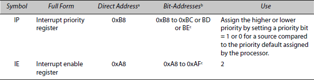
a Address of byte at the SFR.
b Addresses for the bits during set or reset operation on a bit by the SETB and CLR instructions, respectively.
c Number of devices for which ISRs can be provided vary in different 8051 variants.

a SI mode 0 interrupt occurs at the start of data bits. The start condition interrupt enables a read of the bits at the slave using the serial clock and data lines. The occurrence of this interrupt is identified by 1 at the 7th bit in SINT register (an SFR available in few family variants of 8051. SINT is at the address 0xDA). This bit sets on interrupt occurrence. It clears only by a user instruction write to it by a write. PS1 defines its priority and ES1 bit enables it.
Example 3.31
- If IE.3 at 0xAB is set to 1, then what is the action?
The interrupt from T0 overflow is enabled provided IE.7 EA bit at 0xAF = 1.
- If IE is saved with the byte 0x71, then what is the action?
0x71 means 0111 0001. Since IE.7 EA = 0, all interrupt sources remain masked independent of whether other IE bits are 1 or 0.
Example 3.32
If IP.5 at 0xBD = 1 and all other bits of IP = 0, then what is the action?
Serial Interface Interrupt priority becomes high, irrespective of default priorities in Table 3.20.
Table 3.20 gives the ISR_VECTADDR (interrupt vector address) for servicing of the interrupts. A programmer stores the bytes for an interrupt source (or source group) routine and sets the enable bits then on interrupts event the processor vectors to new address and calls the ISR instructions in memory from at ISR_VECTADDR.
Table 3.20 The ISR_VECTADDR (Interrupt Vector Address) where the Programmer Places the Routine for the Interrupt Source (or Source Group) and the 8051 Processor Vectors there and Executes ISR the Corresponding ISR at Code Memory
| Addresses Availablea | Default Priorityb | Explanation of the Function |
|---|---|---|
0x0003-0A |
1 (highest) |
Interrupt vector address for external interrupt at pin INT0. |
0x000B-12 |
2 |
Timer T0 overflow interrupt vector address. |
0x0013-1A |
3 |
Interrupt vector address for external interrupt at pin INT1. |
0x001B-22 |
4 |
Timer T1 overflow interrupt vector address. |
0x0023-2A |
5 |
Serial UART Interface interrupt vector address (common for TxD serial outputs and RxD serial input frames). |
0x002B-32 |
6 |
Interrupt vector address Timer T2 overflow cum T2EX pin negative transition for the time capture or reload at T2. |
0x0053-5A |
7 |
Serial synchronous SI mode interrupt (available in a few family variants). |
a Between addresses, 0x0033 and 0x0052 are left for future expansion. Between 0x0000 and 0x0002, a jump instruction enables run of the boot program. The jump is to boot program starting address in code-memory. It must be after 0x005A is saved.
b The default priorities of column 2 are overridden by the assignments at the IP register bits.
Example 3.33
If IE.4 and IE.7 are = 1, then on setting the TI flag, what are the actions?
SI interrupt are enabled due to unmasking of period port interrupt. On completion of a character or UART frame of 10 T or 11T mode transmission or on reception of a byte or UART frame in buffer for the SBUF, the interrupt takes place. The current program next instruction PCH and PCL are saved on the stack and processor vectors to address 0x23 (Table 3.20). Between 0x0023-2A the ISR instructions for serial interface interrupts exist. On return from the ISR the saved PCH and PCL are retrieved back and the interrupted program runs again.
(2) Servicing of interrupts: Five stages are involved in the occurrence and servicing of an interrupt in 8051:
Stage 1: An interrupt occurs for the processor to interrupt the current process (program) in 8051.
Stage 2: Completes the current instruction.
Stage 3: Checks if EA bit, IE.7 (7th bit of the Interrupt Enable Register), is 0, then processing unit does not recognize any of the maskable interrupts. It continues with the existing program. Maskable interrupt means an interrupt source, which can be enabled or disabled for the service.
Stage 4: If EA is equal to 1, on occurrence of an interrupt, the processor checks whether interrupt for the given source is enabled (not masked) and if yes, then does the following actions:
- Pushes PCH and PCL on to the memory stack. Fetches the corresponding ISR_VECTA-DDR for the source among the seven vector addresses. (Table 3.20).
- Makes EA bit = 0 temporarily until first instruction within an ISR corresponding to the source executes. The further interrupts from any lower priority interrupt are the only ones disabled until return from the ISR. The higher priority ones are polled (checked for pending action on the interrupt) at the end of each instruction in the ISR (Table 3.19). If EA is reset to 0 in any ISR instruction then all interrupts disable. This is done so when running a critical set of instructions. Before the return or after the end of cirtical section in the ISR the EA must be set again to 1 if future interrupts are to be recognised.
Stage 5: Loads into PCL and PCH (program counter address) the start address of ISR (ISR_VECTAD-DR address) and executes the ISR for the interrupting source. The ISR can call another routine. If the 8 bytes ISR space (Table 3.20) available between two routines (two vector addresses) is insufficient, another location routine can be executed by jump instruction to vector to address of remaining ISR.
(3) Sources of interrupts: Intel 8051 family microcontroller has seven sources given in Figure 3.19 that can be masked using the bits in IE. Other sources can be the Timer T2 and I2C serial interface interrupts in P83C528.
The priority of each source (or source group) presets as per Tables 3.19 and 3.20. The user instructions preset the priorities using the IP if the default priorities in Table 3.20 are unacceptable. Source group means a group for which vector address is common and therefore the ISR address is common. Within the ISR, there are different program paths must be provided for each source of a group. For example, the sources— serial transmission and serial reception interrupts belong to same group.
Masking of all or a few sources is done by IE register bits given in Table 3.19:
- The RI and TI flags when set, vectors the program to ISR at a common vector address 0x0023 for them. The ISR then calls the needed routines from memory as per the user instructions. Source needing the service takes the program path according to the ISR instructions at 0x0023.

Figure 3.19 The Interrupt Sources in 8051, Priority and ISR-VECTADDR. A priority is shown in bracket
- When the TF2 flag sets or the external INT2 pin interrupt occurs for capture/reload, then also there is a common vector address, 0x002B for interrupt service. The ISR placed in the memory at this address runs the codes for the source needing the service.
3.9 EXTERNAL INTERRUPTS
Control and Status Bits for the External Sources of Interrupts INT1 and INT0
The following are the control and status bits for the external sources of interrupts INT1 and INT0 at pins P3.3 and P3.2, respectively.
- External hardware interrupts INT1 and INT0 use the four lower bits of TCON given in Table 3.11. When IT1 (INT1 type bit) TCON.2 is reset to 0 the interrupt INT1 is level activated and set to 1, it is edge triggered. It triggers by negative edge (1 to 0 transition) at INT1 pin.
- When IT0 (INT0 type bit) TCON.0 is reset to 0 the interrupt INT0 is level activated and set to 1, it is edge triggered. It triggers by negative edge (1 to 0 transition) at INT0 pin.
- When IE1 (INT1 event flag) TCON.3 sets to 1, the ISR starts and on start of ISR for INT1 service, it resets to 0.
- When IE0 (INT0 event flag) TCON.1 is sets to 1, the ISR starts and on start of ISR for INT0 service, it resets to 0.
SUMMARY
- Microcontroller 8051 family hardware has a CPU that has the ALU, controller and sequencing circuit, program counter, internal buses, address, instruction registers, an instruction decoder and special function registers.
- Pin signals in a 40 pin-member of 8051-family are as per the given Table 3.6.
- The name and address to access the byte and each bit for each SFR are as per the tables.
- The oscillator circuit gives 12 clock pulses for each machine cycle that consists of the states S1 to S6. Each state has 2 clock pulses.
- 8051 operates in two modes—single-chip mode and expanded mode.
- The signals in single chip at the IO pins are P0.0-P0.7, P1.0-P1.7, P2.0-P2.7, P3.0-P3.7.
- Port driving and sink currents must be known for a design of suitable interfacing circuit.
- An open drain port bit of 8051 must first be written 1 before using it as the input.
- 8051 internal program and data memory architecture is unique. It is described for the original family, called classic 8051. Two recently introduced architectures, 8051 extended and 8051MX, have large program and data memory.
- Two bits set the mode of operation in a timer.
- The 8052 family chips have the additional Timer T2. This facilitates a 16-bit timer/counter. There is a capture or a reload feature. T2 facilitates UART operations using the 16-bit timer, or capture of 16-bit time on external input or reload of 16-bit time.
- A member of the 8051 family may possess a watchdog timer. Its’ function is to force a reset after a timeout.
- The serial interface facilitates the synchronous serial and asynchronous UART like serial communication in an instant. Three bits set the mode of operation in the SI.
- A bit IE.7 disables (masks) all the interrupts. The processor fetches the interrupt service routine address. This it does from a the vector address table for 8051 device interrupt source(s).
KEY TERMS
Accumulator. A register usually denoted by A-register, the bits of which are used as the operand in an ALU instruction and which accumulates the result of the operation from the ALU.
ADC or A/D: An internal device to convert analog input into the digital bits after mapping with respect to a voltage reference(s) present in certain 8051 versions.
ALU: An arithmetic and logic unit for 8-bit operations. 8051 has a Boolean processing unit also. It is for the 1-bit boolean or transfer operations.
Architecture of a microcontroller: An architecture is a pictorial description (definition) of the attributes of a microcontroller as seen by the assembly language programmer or compiler writer.
Asynchronous serial communication: Serial transmission or reception in which each byte or frame of bits does not maintain constant phase difference and receiver has the clock to receive the bits independent of the transmitter clock. The receiver clock though is of the same frequency does not have phase synchronization with the transmitter clock.
Auto-reload: A timer starts after loaded with certain specified value and timeouts when this value overflows from all bits = 1 to all bits = 0. Auto-reload means that the specified value loads again automatically on timeout in a timer mode. The timer thus restarts and timeouts at successive pre-fixed time intervals. On each timeout, there is reload and there is the timer overflow interrupt.
B Register: A register, the contents of which are used as the operand in 8051 ALU multiplication and division instruction and which also accumulates the 8-bits of the 16-bit result of the operation.
Bank: A set of registers in 8051 internal RAM defines a bank. [For details, refer meanings of Code Bank and Register Bank also.]
Baud rate: Rate by which the bits trickle on an UART serial line.
Carry: A flag (bit which sets or resets on an event) to indicate that addition of two numbers exceeded the register capacity to hold that number. Register will now hold the excess value over that. A borrow is also indicated by the carry in the microcontrollers. The carry bit is also used like the accumulator of 1 bit in the Boolean processor operations in 8051.
Clock: The pulses, which are the inputs to the control and sequencing unit of the processor. It also gives the inputs (as such or after pre-scaling) to the timer(s) after division by 12 in 8051.
Clock circuit: A circuit to generate the clock pulses and states in the processor using the external crystal or internal oscillator element. (Refer figure 2.17)
Code bank: A concept for a set of 2 kB codes at the memory to enable division of the code into the various segments of the program — memory.
Counter: A device to count the successive inputs (for the events) to it. Timer differs from it only in the sense that (i) timer is preloaded with certain number of ticks (counts) (ii) timer is given inputs at the successive time intervals using a clock circuit (iii) appropriate division of clock pulses takes place before they are given to the timer. Both counter and timer overflow and interrupts on a transition from the maximum value to minimum value.
Cross talk: The induced signals at a neighbouring the line when the lines are improperly isolated from another circuit line.
DAC (D/A): Digital to analog conversion to obtain a maximum equal to the reference voltage when all inputs are 1s and minimum when all inputs are 0s. Microcontroller has a PWM (pulse width modulator) device. The device provides the DAC action on integrating the PWM output.
Decoupling capacitor: A capacitor placed between the supply rails (parallel thick lines) to a digital IC. It is placed as close to the IC as possible. It decouples from the supply lines the line noise signals. The noise is induced due to sharp transitions within the IC.
Down counter: A counting device which decrements on the successive event inputs. Number of ticks preloaded in it multiplied by the time interval between the inputs gives the timeout period from the down counter. Microcontroller has up counter not down counter.
DPTR: A 16-bit register, which is saved an address so that it later points to an external data memory address in the subsequent instructions.
E Code: Codes placed at the external memory in the 8051 extended architecture.
Expanded mode: A mode of 8051 in which it interface with the external devices using the port pins.
External interrupt: An external device signal, which when activated and when the source is not masked, causes the execution of an interrupt service routine.
Free running counter: A counter starting from the system start and counting the clock pulses endlessly. Its features are— it is non-stoppable and non-reset able and therefore usable in real-time applications. It generates interrupts on periodic overflows. It can be read at an instance but cannot be written.
Full duplex: Facility to simultaneously transmit and receive the bits. It is done on two independent serial lines.
H-Data: The data on the external memory space in the 8051 extended architecture.
Input capture: A mechanism in which the number of ticks at a counter (timer) are saved into a register on an input event for example, 0-1 or 1-0 transition or toggling input and an interrupt is also generated to call interrupt service routine.
Instruction cycle: A cycle of one or more machine cycles to complete an instruction at the microcontroller.
Instruction decoder: A register the contents of which initiate the actions of controller and sequencer circuit actions. The action sequences are per the instruction opcode received at the IR register.
Instruction register (IR): A register to receive the opcode before the instruction executes in the processor.
Internal program-memory: Memory to store the program, constants, interrupt service routines (ISRs) and interrupt-vector address ISRs.
Interrupt: An action, which causes the diversion of the program to another routine called ISR (interrupt service routine) on occurrence of an event. For example, timeout (overflow), input capture, out-compare, serial byte transmitter empty, receive buffer full, external input, etc.
Interrupt enable register (IE): A register to hold the bits, which disable (mask) all or and enable the individual interrupt sources (source groups).
Interrupt mask: A bit to disable the recognition of an interrupt source.
Interrupt mechanism: A mechanism to enable the servicing of the interrupt in a processor.
I2C serial bus: An inter-IC serial bus with two signals— serial data and clock.
Interrupt priority: When a number of events occur and pending the execution of ISR, the priority resolves the issue of which one to service first.
Interrupt source: A source of an event, which causes the program diversion to an interrupt service routine like a function call in the program. An event example is timeout (overflow) of a timer.
Out-comparison: An action in which timer values are compared with certain value loaded in a registers and as soon as time value becomes equal to that then an out-compare interrupt occurs and also an output pin sets or resets or toggles as per the programming for the out-compare action.
Open drain: A port in which a drain terminal of the output gate not connected internally to pull its voltage to VDD. The port bit can thus be at 0 only unless some external pull up circuit is connected to it.
Polling: A mechanism in which it is found out which device or source needs the service or is active by successively probing in a sequence.
Processor status word: A word or 8-bit in 8051 at an SFR which saves the flags (the one bit result of an ALU operation, for example, carry or borrow set in addition or subtraction). It also saves the user defined flag(s) and saves the bits that define the register bank for the subsequent instructions.
Register bank: A set of eight registers in the 8051, which is selected in an instruction according to the RS0 and RS1 bits at the PSW prior to the use of registers of register-bank.
Reset: Processor setting the default values in the registers as on the power up and start execution from 0x0000 address at the program counter (PC).
Reset circuit: A circuit in the microcontroller, which makes the reset pin low first and then high for the specific periods.(figure 2.16) During these periods, the processor resets. Pin RESET is input to start with and becomes output for a specific period. The reset-output state enables associated interfacing devices like 8255 to reset in synchronization with the processor reset.
ROM: Read only memory.
Serial interface (SI): A device, which enables serial transmission from 8051 when a byte is written into SBUF and serial reception when SBUF is read. The device modes are as per the SM bits. SCON controls the desired function(s) of the SI.
Single-chip mode: A mode in which the internal hardware is used and ports P0 to P3 are used as port latches.
Special function register (SFR): A special register in 8051, which can be read, written, or operated by an 8-bit operation of instruction. Each bit in certain SFRs can also be read or written or operated by a 1-bit operation instruction.
Stack pointer: In 8051, it is eight-bit register, also an SFR, which points to the stack of the program being executed. Default value on reset of processor is 0x07.
Synchronous serial communication: Serial transmission or reception in which each byte or frame of bits maintains a constant phase difference and receiver has the clock to receive the bits dependent and in phase with the transmitter clock. The receiver clock though is of same frequency as well as phase synchronized with the transmitter clock. The synchronous communication is serially shifted register (SBUF) output by a shift-clock in SI of 8051.
Timer: A device in 8051 (a) which can timeout (after a preset time interval) or (b) which can count the external inputs or (c) which can be externally controlled or only software controlled for the start or (d) which can reload automatically or by the instructions or (e) time can be captured at an external instance or (f) which can be compared with respect to preset time for alarm like event generation or (g) which can control the baud rate for the SI.
Timer overflow: A timer starts after being loaded with certain specified value and timeouts when this value overflows from all bits = 1 to all bits = 0. The value increments on each successive count input to the timer. On each timeout called overflow, there is an interrupt event.
Timing diagram: A diagram to show the relative timing of activation and deactivation (also set 1 or reset 0 states and the various signals with respect to the clock states. It helps in understanding, which transitions occur first and what is the sequence of signals on the buses.
X-data: The data placed in the external data memory space of 64 kB.
Watchdog timer (Timer T3): A timer which resets the 8051 after the preset time so that program stuck up in the middle due to certain event can get out of that situation. WDT can be rewritten before timeout to extend the resetting period.
Z-flag: A flag (not present in 8051), which sets when result of an operation causes results in which all bits become equal to 0.
REVIEW QUESTIONS
- Draw the architecture of 8051.
- What is the use of DAA (decimal adjust accumulator) unit with an ALU? Why are there two registers—A and B in 8051?
- What are the resources available at the 8051 as an enhancement of 8048?
- List the addition devices (include the memories) that are present in the 8051 in comparison to the microprocessor.
- Why is a microcontroller also called a microcomputer?
- List the alternate uses of each pin available in 8051 when used in the expanded mode.
- Explain the uses of each PSW bit in 8051. What are the flags that associate with ALU operations in 8051?
- What are the pointers in 8051? Which ones are at the SFRs? Explain the uses of each pointer. Explain the ‘stack’ feature in 8051.
- Explain the meaning of each bit in SCON and SMOD registers. What is the use of the SBUF register?
- Explain the meaning of each bit in TCON and TMOD registers.
- What are the modes in which SI (Serial Interface) can be programmed to use in 8051?
- What are the modes in which T0 and T1 (Timers 0 and Timer 1) can be programmed to be used in 8051?
- How do you use the timer 0 as a counter of external events?
- How do you use an external gate pin to start a timer in 8051?
- What are the advantages of synchronous communication in conjunction with the TR bit? What are the advantages of UART communication?
- When do you use 10T UART mode 1 and when 11T UART modes 2 and 3?
- Explain the oscillator outputs in terms of clock pulses and their periods and in terms of the states in 8051.
- Explain the RESET mechanism in 8051. What is internal reset? What is external push button reset? What is power-up reset and what is watchdog timer reset?
- Describe the voltage levels and the current source and current sinks in the LSTTL and CMOS gates.
- Describe the memory for the data and SFRs in 8051. What are the addresses to access the bytes at different areas of memory? What are the addresses to access the codes at the different areas?
- Describe the memory for the data and SFRs in 8051 extended. What are the addresses to access the bytes at the different areas of memory? What are the addresses to access the bytes at the different areas?
- Describe the memory for the data and SFRs in Philips novel architecture 8051MX of unified address space for data and program. What are the addresses to access the bytes at the different areas of memory? What are the addresses to access the codes at the different areas?
- Explain the PCON register bits.
- Explain the meaning of an interrupt vector. What are the interrupt vectors available in 8051?
- What are the hardware assigned default priorities in various interrupt sources of 8051?
PRACTICE EXERCISES
- Show the signals at the 8051 pins. Explain meaning of each signal. Also, indicate when a signal is input and when output. What are the signals multiplexed at the port P0? What are the signals multiplexed at the port P3?
- Explain the 8051 pins/signals, which have different meanings at different instances.
- How do you program the timer 0 using corresponding SFRs?
- How do you program the timer 1 using corresponding SFRs?
- How do you program the timer 2 using corresponding SFRs?
- There is a mosquito trap which generates an active low transition on each trap of the mosquito. How will you use an 8051 timer to find the number of traps in one hour?
- There is a motor which generates an active low transition on each revolution. How will you use an 8051 timer to find the rpm (revolutions per minute)?
- There is a motor which gives a feedback input on each completion of a revolution. How will you use the 8051 external interrupt pin to find the number of revolutions in one hour?
- How will you generate a pulsed output every 2 ms using 8051 with a 12 MHz oscillator?
- How do you program the synchronous communication using corresponding SFRs?
- How do you program the synchronous communication using corresponding SFRs?
- How do you program a watchdog timer in 8051?
- How do you program the IP and IE registers?
- How do you disable the use of internal program memory codes in 8051? What is the use of that?
- Explain the difference in the memory architectures in 8051, 8051 extended and 8051 MX.
- Explain uses of TB8 and RB8 bits in 8051.
- How is the baud rate for UART serial communication programmed in 8051 using the T1? What is the advantage of using T2 in 8052 family for the serial communication?
- How are interrupt vectors used to service the timers, serial transfer and external interrupts in 8051?
- Explain how you would override the priorities using the IP register by the example of assigning serial interface as the highest priority interrupt source.
- How will you mask the use of serial interface?
- Explain how 8051 microcontrollers will communicate the data on the common TxD and RxD lines in the interprocessor communication mode.
- Explain the timing diagram in Figure 3.9.
- How will you set the watchdog timer to restart the processor at every 2 ms?
- How will you use the 8051 serial interface to send the ASCII characters for your name on the TxD line?
- How will you use the 8051 serial interface to send the ASCII characters for your name on the TxD line with 300 characters per second baud? What will be time taken to send all?
MULTIPLE CHOICE QUESTIONS
Consider 8051 family microcontroller in the following questions
-
- A, B and PSW
- A is accumulator, only B and PSW
- PSW is not among ones, which
- None of the A, B and PSW
are the special functions registers
- Number of ports used in an expanded mode are:
- two
- three
- four in case of additional devices present in a family member
- depends according to the use of external program memory or on use of external as well as data memory
- RS0 and RS1:
- are not in the PSW as these are not the flags
- are in the register sets (banks)
- are the bits-4 and 5, respectively, for selecting the register bank in the PSW
- are the bits-3 and 4, respectively, for selecting the register bank in the PSW.
Note: Bit 7 is C (carry or borrow) flag
-
- We can use a common memory chip for the program and data, ifwejoin the and pins
- If we join the and pins, the 8051 will not save the program at external memory
- If we connect pin to Vcc then we cannot use the external program memory
- The 8-bit address of a byte as 0x00 refer to internal RAM if = 1 and external RAM if = 0
- We can use a common memory chip for the program and data, ifwejoin the
- Reset pin is:
- active when connected to 1
- active for a few cycles only
- active when connected to 0
- active only on watchdog timer reset
-
- Port P0 can be used as an output only because it is used as AD0-AD7 in the expanded mode:
- All port bits can be used as input or output in single-chip mode
- A port bit can be used as an input after writing 0 at it
- Two ports P0 and P2 are the output ports and P1 and P3 are the input ports:
- Bit address 0x00 and byte address 0x00 are for the:
- Bit 0 at 0x20 and the byte at 0x00 in the internal RAM
- Bit 0 at 0x00 and the byte at 0x00 in the internal RAM
- Bit = 0 in a SFR and the byte = 0x00
- Bit 0 at 0x20 and byte at 0x00, respectively
- TH1, TL1, TH0 and TL0 SFRs are at the addresses:
- 0x8D, 0x8C, 0x8B and 0x8A
- 0xAD, 0xAB, 0xAC and 0xAA
- 0x8D, 0x8B, 0x8C and 0x8A
- not between 0x80 and 0xFF as these are not the SFRs
- Mode bits M1 and M0 can:
- be set as 11 at TMOD.5 and TMOD.4 and get assigned to TH0 as an 8-bit timer
- be set as 00 only
- can be set as 00 and 10 only
- not be set as 11 at TMOD.5 and TMOD.4 because timer 1 does not function in mode 3
- Timer 1 runs and timer 0 stops:
- when TCON.6 = 1 and TCON.4 = 0
- when TCON.4 = 0 and TCON.5 = 1
- when TCON.7 = 1 and TCON.5 = 0
- when TCON all bits are 1s
-
- Synchronous mode of operation of serial interface can either be to transmit or receive at a given instant
- asynchronous mode of operation of serial interface can only either be transmit or receive at a given instant
- synchronous and asynchronous mode of operation of serial interface can be transmit and receive at a given instant
- only asynchronous 10T period and 11T periods exist in the serial interface using TB8 and RB8, bits
- When SM2 is set to:
- 1, it facilitates the multiprocessor communication in case of mode 1 and 3 (variable baud rate serial UART mode)
- 1, it facilitates sending the address for the multiprocessor communication in case of mode 2 and 3 (total 11 bit serial UART mode)
- 0, it facilitates the multiprocessor communication in case of mode 2 and 3 (total 11 bit serial UART mode)
- 0, it facilitates the multiprocessor communication in case of mode 0 only (synchronous communication mode)
- If a period is 0.33 ms between the serial bits, we can transfer in one second when SCON sets for mode 2:
- 300 characters
- 275 only
- 30 characters
- 272 characters
- At the RS232C because of the need to provide a margin for the attenuation and noise pickups:
- 0 means + 3V down to + 25V
- 0 means + 5V down to + 25V
- 1 means + 3 V down to + 25 V
- 1 means + 5 V down to + 12V
- IP.4 is set to 1 in the interrupt priority register:
- synchronous serial communication mode priority becomes highest
- timer T1 priority becomes highest
- interface serial communication mode priority becomes highest
- synchronous serial communication mode priority becomes lowest
- If IP register has been set as 0x00 then:
- INT1 has the highest priority
- INT0 has the highest and serial interface as the lowest priority
- timer overflows have the highest priorities
- there is no priority, interrupt processes in the order of its occurrence
FILL IN THE BLANKS TYPE QUESTIONS
- 8051 has internal ROM memory for the _____.
- There are four _____ in 8051.
- External interrupt pins _____ are and _____.
- Bit 7 of PSW is _____ and bit 2 of PSW has bit-address _____.
- PSW bits are 00100001. It means _____.
- TxD signal is at _____ pin and RxD at _____.
- Single-chip mode is used when _____.
- ALE signal is for _____ and is present during _____ states of the clock.
- P3.5, P3.6 and P3.7 pins alternative uses are _____, _____ and _____, respectively.
- Timer T0 mode 3 is used when _____.
- TMOD register bits are 0100 0100. It means _____.
- TCON bits are 0000 0000. It means _____.
- Serial communication mode 0 is used when _____ and bit transmission rate in this mode is _____.
- SCON bits are 0100 0000. It means _____.
- Formula for calculating period of one serial bit in mode 3 is _____ where _____ means _____ and _____ means _____.
- UART communication in 8051 takes _____ time slots in mode _____.
- Serial receiver interrupt enables when _____ and _____ bits are _____.
- Two interrupt vector addresses have _____ bytes addresses between them to enable _____.
- When there is UART transmission interrupt, the interrupt service routine executes from address _____ and the service routine code must be less _____ bytes. The ISR code can be extended by _____ instruction in ISR.
- When there is UART receiver interrupt and INT1 pin interrupt, then _____ has higher priority if _____ and _____.