
4
8051 Family Microcontrollers Instruction Set
Chapter Outline
- Learn programming basics and introduction to machine and assembly instructions
- Different types of instructions and addressing modes in the instructions
- Learn the data transfer, byte arithmetic and logic operation instructions of 8051
- Learn the data and bit manipulating Boolean processing, program control, IO and interrupt control instructions of 8051
- Write simple assembly language programs using 8051 instruction set
- Write simple programs for data transfer, delay and use of loops to understand the instructions
4.1 PROGRAMMING BASICS
A program means a set of instructions, which executes in an order. The order of execution of instructions is defined in the program. Many instructions in a program execute in a sequential order.
Each program has a start address. There is always the first executable instruction of program at the start address of a program. An end instruction can be for reset or halt or jump back to the same instruction or return (to the calling program or routine). The CPU fetches and executes from the start address the first instruction of a program or routine, then the next, then the next, and so on till the halt. Machine codes mean bytes that are fetched and executed by the CPU. Each memory address has 1 byte.
4.1.1 Machine Codes
A CPU recognizes only Is or Os. Every distinct instruction, which is executable on a CPU, has a distinct sequence of Is and Os in each byte of the instruction. A sequence of Is and Os is called a machine code. Each program consists of the instructions. The bytes that are saved in the memory for the instructions are called machine codes.
Consider the instruction for adding R1 into A registers. It is written as ADD A, R1 in mnemonic form. First source operand is R1. The second source operand is A. The destination is also A. It has a distinct machine-code 0x29 (also written as 29H to indicate that 29 is byte in hexa-decimal) of just 1 byte in 8051. (By convention, in 8051, the destination or the second source operand is written first and the first source operand next. Therefore, A is written first and R1 next after the ADD.) The instruction gives the result of adder operation in A and processor status, for example, carry C in PSW.
Assume ADD A, R1 is an instruction at address 0x4000. Since the instruction machine code is 29H (hexadecimal number for binary 0010 1001), the 0010 1001 saves as machine code at address 0x4000.
Example 4.2
Consider the instruction for jump to a long (16-bit) address 0x0100. It is written as LJMP 0x0100. It has a set of three distinct codes 02H 00H 01H at three addresses. (By convention, in 8051, the lower byte saves at the lower address and the higher byte is at higher address after the byte for the opcode. Therefore, 00H is first and 01H is next after the opcode 02H.)
The instruction is in the form of a byte (or bytes in case of longer than 8-bit instruction). A CPU first fetches a machine code from a memory address. It stores the code in IR (instruction register). It decodes the IR code. It then reads the operands of the instruction. Then that instruction executes. The fetch and execution steps for the machine codes of instructions are controlled by the controller and sequencing circuits (Fig. 3.1). The results are written after execution finishes. The CPU then fetches the new instruction for the next cycle of fetch-execute.
Each CPU on power up defines a start-up value of the program counter (instruction pointer). The CPU starts fetching the machine codes from that address. The start-up program counter value is 0x0000 (0000 0000 0000 0000b) in 8051.
Example 4.3
Assume that the initialization-program’s instructions (called boot-up program) start from 0x0100. Figure 4.1 shows the memory addresses in program memory and arrangement of the machine codes of the programs in 8051 in this case. The processor fetches the first instruction from 0x0000. Second instructions will be machine codes of boot-up program at address 0x0100. From then onwards the program’s instructions start executing. Figure 4.1 shows that first there will be machine codes at 0x0000, 0x001and 0x0002 for jump to 0x0100.
The reason that the boot-up program is starting from 0x0100 in the above example and not from 0x0000 is as follows:
- Between 0x0003 and 0x000A the 8 addresses should have machine codes for interrupt service routine for external interrupt INT0.
- Between 0x000B and 0x0012 the 8 addresses should have machine codes for interrupt service routine for external interrupt T0 overflow.
- Between 0x0013 and 0x001A the 8 addresses should have machine codes for interrupt service routine for external interrupt INT1 overflow.
- Between 0x001B and 0x0022 the 8 addresses should have machine codes for interrupt service routine for external interrupt T1 overflow.
- Between 0x0023 and 0x002A the 8 addresses should have machine codes for interrupt service routine for external interrupt serial interface TI (transmitter interrupt) and RI (receiver interrupt).

Figure 4.1 The memory addresses in program memory and arrangement of machine codes of the programs in 8051
Refer to Section 3.8 to find out why these addresses are used for interrupt servicing. After the interrupt service routines, there can be a blank space or constant data for program parameters up to 0x00FF. (0x00FF is the address just before the boot-up program at 0x0100.)
4.1.2 Program as a Set of Instructions and Routines
A program consists of a set of instructions. A program instruction may be for calling a routine (another program, a sub-program). A routine is another set of instructions at another set of start and end addresses. A program may also have a number of instructions to call the number of routines in between. A routine may also have an instruction to call another routine. A program or routine can also be interrupted and a new routine called ‘Interrupt Service Routine’ executes.
Routine: When an instruction calls a routine, the program counter for the next instruction I of the program saves and the CPU loads the program counter with the first instruction address of the routine. When the return instruction in the routine executes, the CPU loads the program counter for I.
Routine (subroutine) is a program or a sub-program. It is required by a program for executing a certain set of instructions. The CPU returns to the calling program instruction I after return. Each program or routine has the starting and end addresses. Figure 4.2(a) shows three memory areas for one program for an application and two routines for the same application. It shows three areas for the constants needed by these three as the input data.
Interrupt Service Routine: When an interrupt occurs, such as timer overflow, a new routine executes. That is called an interrupt service routine because it services (handles) the interrupt. Program counter for the next instruction of the present program saves and the CPU loads the program counter with the first instruction address in the new routine. When the return instruction in the ISR executes, the CPU loads the program counter back to enable previous program to run again.

Figure 4.2 (a) Three sets of the machine codes in three memory areas for one program for an application and two routines for the same application. Also shown are the three areas for the constants needed by these three as the input data. (b) Op-code and operands in four exemplary types of instructions
The program or routine or interrupt service routine, consists of a set of the machine codes stored as the bytes at the memory. The program runs by a sequence of executing codes.
4.2 INTRODUCTION TO MACHINE INSTRUCIONS AND ASSEMBLY
Programming in the form of machine instruction-codes is very difficult. The codes are in large numbers for the large number of instructions needed in a program. Therefore, programming can be done easily in the assembly form of the codes of the instructions or more easily in C language.
The following is a convention for the assembly format. Prefix 0x or Postfix H is used to indicate a hexa-decimal number, b to indicate a binary number and none to indicate a decimal number when writing an instruction. Destination operand in 8051 is written first after the operation specification. Prefix # is used to specify an operand, which is called immediate and is the succeeding byte(s) within an instruction.
Figure 4.2(b) shows the opcode and operands component in four exemplary types of the machine instructions. It is similar to an example tan 9. Here, tan defines the operation. It finds the tangent (ratio of perpendicular and base) to an angle. 9 defines the operand for the angle. Similarly, an assembly instruction has two components—opcode and operand(s). [Halt instruction has no operand.]
Instructions in assembly-language program are in the mnemonic form for the machine codes. Examples 4.1 and 4.2 give two mnemonics forms, ADD A, R1 and LJMP 0x0100.
4.2.1 Opcode
Each CPU defines a distinct set of instructions that distinguishes it from another CPU. It defines all the operations possible on that CPU. Therefore, each CPU has a distinct set of opcodes and one opcode for each distinct operation permitted by the CPU.
An opcode means the operation code.
Example 4.4
An operation may be as follows—add two registers and place the result back into one of the registers (ADD A, R5). Another operation could be add a register A with a constant number 8 (ADD A, #08). Both operations need distinct sequences of operations inside the CPU. Hence, both will have distinct opcodes for the ADD operation. One will have opcode for the add register into the accumulator and another for ADD immediate. Note that add-with-carry will have different op-codes and add-with-memory a different opcode. A and R5 are the operands in the first instruction and 08H is the operand called immediate operand in the second. The prefix # is an abbreviation for the immediate operand byte or number.
Example 4.5
Consider MUL AB. This is for multiplying the A and B register contents (bytes). It places the result into a set of two registers—A and B themselves. This instruction has the separate opcode from ADD registers or Add immediate. This is because MUL has a distinct set of CPU-operations. In this instruction, A and B are the source operands as well as the destination operand.
The CPU first fetches the code from an address. In fact, the byte fetched first is first examined for the opcode by the ID (Instruction Decoder). (The byte may have all the bits or few of the bits for the opcode.) Then, the code stores itself in IR so that the associated ID decodes it. Then only, the processing unit does the necessary operations using the controller and sequencing circuits (Fig. 3.1). The CPU operations after the opcode may also need subsequent further fetch of the operand(s)—the ones corresponding to the instruction in order to execute the instruction as per the opcode. It needs the program counter (which is also the instruction pointer) increment to change to another so that when all the CPU internal operations or actions are over, the CPU can fetch the next instruction from the newly pointed address by the program counter.
4.2.2 Operand
The CPU most often needs also the operand or operands in order to perform the operations as per the opcode. Let us consider that an opcode is for a transfer of the data byte from one register to another. Transfer means copy the bits. It is denoted by MOV in 8051 data transfer. Assume that opcode consists of just two bits and the instruction is MOV R1, R2. The 8051 instruction set convention is for specifying destination operand first and then the source. It means transfer (copy) R2 bits into R1.
- There is a need for an operand after the opcode for MOV instruction. That defines the destination where the data bits are to be moved, which actually means copied.
- There is a need of another operand. The instruction defines the source from where the data bits are to be taken. These registers are the ones usable by the programmer. (Source register R2 can be specified by three bits 010 if there are eight registers in the CPU. R1 is also specified by 3 bits010.) R1 and R2 are specified by 6 bits. Total instruction length is 2 + 6 = 8 bits (1 byte).
The total instruction code will consist of the opcode bits for register-to-register data transfer and two set of bits for the two operands. (Total of 8 bits (1 byte) is thus the instruction-length.)
The operations are performed on the source or sources. These are defined in the operands of the instruction. The result is saved at the destination, which is also defined by an operand. However, certain operands may be self-implied for an operation. Consider Example 4.1 ADD A, R1 instruction. The bits for representing R1 form one operand and the bits for the A form another operand. The third operand needed for defining the register A to place the result is self-implied by the CPU.
Example 4.6
Consider another operation for the SUBB A, #08H instruction (subtract-with-borrow and immediate 08H.) The bits for representing A form one operand and the bits for constant number 8H form another operand, called immediate operand because of the immediate availability of it as a succeeding byte in the instruction. The third source operand is carry flag. (Carry flag for addition is also used as borrow flag in 8051 subtraction). Fourth operand is needed for defining the destination register for the result. Both third and fourth (C in PSW and A) are self-implied in the CPU operation for SUBB.
The 2-byte instruction SUBB A, #08H consists of opcode bits for the subtraction with borrow immediate to register, and two set of bits for the two operands—one for the accumulator register and one for immediate.
4.2.3 Register
A register is a named entity. Each register in an MCU, or programmable-controller or device is assigned a name as per basic function(s) assigned to it in an instruction. P1 is a special function register in 8051. Its function is to function as input register and output register for the port P1 register. Consider two equivalent instructions in 8051—INC P1 and INC 90H. Both happen to be of 2-byte length and both increase the byte at P1 by 1. This is because in 8051, the direct address of P1 is 90H. However, when we write P1 in mnemonic form in place of 90H, it is easier to remember when programming. Operations possible on the registers are as follows:
- A register can store a variable or temporary variables that are directly and internally used by the processing units. A byte at a register has easy accessibility by the processor compared to the one at an external memory. External-fetch or store takes more time than an internal access by a processor. Consider the operation, a * b. A and B registers in 8051 store two temporary variables, a and b before the multiplication by MUL AB instruction or division by DIV AB instruction. MUL AB and DIV AB are just 1 byte long instructions.
- A large number of registers can load a larger number of program variables. The use of the registers greatly reduces the external memory accesses. The external accesses take a longer time than the internal accesses. 8051 has 32 registers distributed in four banks (sets).
- The number of register sets (banks or files) can load the variables in the different register sets in different tasks or routines or interrupt service routines. It greatly reduces the number of pushes and pops of the variables when the context switches on a call or interrupt. The 8051 has four banks (sets), and each bank can be assigned to separate routines or tasks. (The term context means a program’s present set of registers, program counter, stack pointer, A, PSW and other variables. When a program changes and another routine executes, we can say that the context has switched to another. When there is a return, we can say that the context has switched back. The term task is used in the operating systems. A task is a function the state of which is controlled by the OS and context switch from one task to another is also controlled by the OS.)
- A register can be assigned a specific action. For example, register A is assigned the role of an accumulator. It is also called ACC. ACC is used by the ALU in the accumulation of the result (for example, after increment, addition and logical operation). Consider 8051 instruction, SWAP A—it swaps (exchanges) lower and upper nibbles and the resulting byte accumulates in A itself.
- Each bit or set of bits of a register may have the specific and distinct action. Each bit of the n bits may be used together or separately. It all depends on the instruction. For example, statusregister (processor status word) bits in the MCU. Other examples are bits at (i) the mode register, TMOD (ii) the control registers, TCON and SCON.
- Each half (byte or nibble) of a register may have a specific and distinct action. Assume that the number of register bits is n. Then, n usually equals 8, 16 or 32. A register lower significance n/2 bits and higher significance n/2 bits may be usable simultaneously or separately in programming. It depends on the instruction.
- Each nibble or byte or 16-bit word or 32-bit double word in a register may have the specific and distinct action. Let n = 32. The lower significance n/2 bits, higher significance n/2 bits and two lower significances set of n/4 bits may be used together or separately. It will depend on whether an operand in the instruction is of 32 bits, 16 bits or 8 bits, respectively.
- A register can store a pointer (an indirect address or indirect address bits) for internal or external memory. Some examples make use of Ri and DPTR (DPH-DPL) in 8051. (Exemplary instructions are MOV A, Ri and MOVCA, A + DPTR). These instructions are explained later.
- When using a register, the few bits of operand suffice in the instruction. When using the register the instruction length may be shorter. When using a memory address in place of the register, the operand is of 8 bits or 16 bits for the address. For example, consider the register A. The 8051-instruction INC A is of 1 byte length. Now, consider an instruction INC direct with direct address—0E0H. The instruction length is 2 bytes. (The opcode is of 1 byte and address of 1 byte.) Both instructions are different but have equivalent actions except the number of times the program counter increments after the instruction executes. (In 8051, the direct address for A register is 0E0H.)
Figure 4.3 shows the many uses of a register during programming. A 1-byte register saves like a memory-address.
A programmer uses the registers in a large number of instructions. The use of a register differs from a memory in the following respects: Use of register makes the instruction-length small. When using memory the instruction-length is more. This is because address of the byte(s) in memory needs to be defined in the instruction. The increased instruction length increases the fetch-execution cycle time of the instruction.

Figure 4.3 Multiple uses of the registers during programming
4.2.4 Accumulator
A processing unit can be one address machine. It means that most instructions, particularly the ALU in-structions need only one operand definition in one address machine. The remaining operands are implicit. One address machine uses an accumulator. The accumulator (denoted by AC or ACC or A) is a processor register that accumulates result from an arithmetic or logic operation. Further, the accumulator also acts as the source operand in an instruction. Design of the processing unit with one address machine simplifies a processing circuit and internal control circuitry greatly. It reduces the maximum length as well as the number of the opcode bits in the instruction set. The programmer also finds it easy to assemble the codes. The accumulator can also accumulate a value from an external input port or memory and source a value to an external output port or memory. Examples are MOV A, P1 and MOVP1, A.
4.2.5 Program Counter
It is an address pointer for a code. It controls the flow of the program. It is abbreviated as PC in 8051. Right from the start of the processor, it always points to the next instruction to be fetched. During a task or routine, it usually increments continuously like a counter after fetching each byte of instruction. Figure 4.4 shows that the program counter changes to the next instruction address first. It takes a new value only on jump or call for another instruction or routine or return from a routine. It takes a default reset value on the reset instruction.

Figure 4.4 Program counter (or instruction pointer) initial values in 8051, 80x96, 80x86 and 80960 and the vector address for the program counter in 68HC11
- There is a default value that resets at start (power up). The value can be the same as the value on reset by hardware and software (for example, 8051) or can be distinct (for example, 68HC11).
- There are the distinct values at which it resets for the different interrupt vector addresses.
- A multi-process system will have multiple program counters and each process program counter has its distinct initial value. A multi-processing or multi-tasking or multi-threading system in a single-processor system will have multiple initial values of the program counter, distinct for each process or task. (The terms—thread, process and task are used in the operating systems. These are explained later in Chapter 11).
Figure 4.4 also shows the program counters’ initial values in 8051, 80x96, 80x86 and 80960. There is a vector address for the program counter value on reset in 68HC11. A programmer programs the 16-bit of the vector address. The program vectors to that value on reset on power up.
4.2.6 Stack Pointer
It is an address pointer for a memory address called stack top. It is abbreviated as SP in 8051. It is abbreviated as S in 68HC11. The SP points to a current stack top address. Stack is an important data structure. Data when saved (pushed) are stored in a manner that can be retrieved (popped) as last in first out (LIFO). The stack facilitates a programmer to save LIFO retrievable data. A stack is accessed from the memory in the LIFO mode, while a row of data in the queue is accessed in a FIFO (first in last out) mode.
Suppose, the processor saves the current program counter (calling program code address) onto the stack top, on return from the routine where the processor pushed that address earlier can be popped from the stack top and the program will switch back from the called program (routine) to the calling program.
- The SP increments (or decrements, depending on the processor design) after (or before, depending on the processor design) the push of each byte. Before a push, the pointed address at SP increases. Stack top is at the address 1 above the SP-pointed address in 8051.
- The SP decrements (or increments, in the processor design in which the push decrements it) before (or after, in the processor design in which during the push the SP change is before) pop of each byte. After a pop the pointed address at SP decreases in 8051.
- The memory addresses between the current stack top and original stack top at the start (stack bottom) hold the pushed bytes (for program counter or program variables or data) (Figure 4.5(a)).
- There may (for example, 8051) or may not (for example, 80x96 and 68HC11) be a default SP or S value which resets like the PC value on the start (power-up) in a processor.
- A multi-process system will have multiple stack pointers and each process stack pointer has its distinct initial value. A multi-process or multi-tasking or multi-threaded system in a singleprocessor system will have multiple initial values of the stack pointer for each process or task.
Figure 4.5(b) shows the stack pointer initial values and use during push and pop in 8051, 80x96, 80x86, 80960 and 68HC11. SP has 8 bits in 8051 default value = 0000 0111b (hexadecimal 07H), and 16 bits in 80x96 and 68HC11 (called register S in place of SP). S has no default values on the reset or power up in the processor. SP (stack pointer) has 16 bits in 80x86 and is used in conjunction with another register, called the segment register. 80960 has a 32-bit stack pointer called r1 register of the set of 16 local registers. ARM MCU uses r13 as the SP of 32 bits.
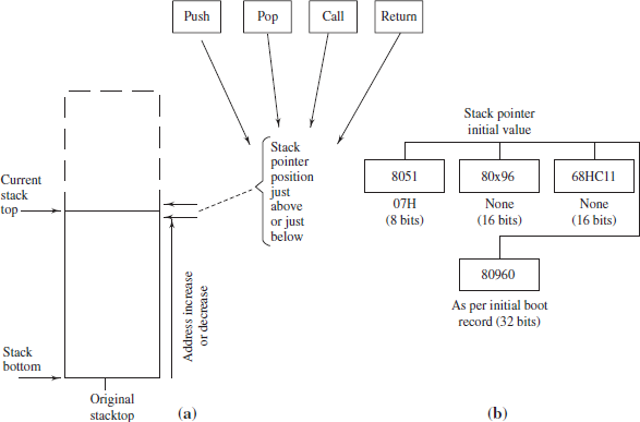
Figure 4.5 (a) Memory addresses between the current stack top and original stack top at the start (stack bottom) and (b) Stack pointer initial values and use during push and pop in 8051, 80x96, 80960 and 68HC11
4.2.7 Program Status Word
A processor or program status word register is one of the most important registers. It is abbreviated as PSW in 8051. It is invariably present in each processing unit for the programs.
A PSW has many bits. Either none or only a few pairs of bits may relate. A bit shows a certain condition of the process and so it is also called a flag. Carry auxiliary carry and zero flags are examples. Carry flag is used in all processors to implement multiple times addition or subtraction and there is use of carry (or borrow) in addition and subtraction. We can add or subtract multi-digit numbers multiple times by the carry. When a carry is generated in the arithmetic operation, the future arithmetic operation may depend on that. Therefore, the carry reflects the status of the process (or program). Note that the carry flag itself is used to show a borrow during subtracting.
An auxiliary carry flag is used in all processors to implement BCD additions. A condition that a carry results by addition of the lower nibble is saved in a bit called the auxiliary carry flag. A condition that a borrow results by subtraction of the lower nibble is saved in a bit called the auxiliary carry flag. Flag such as overflow is explained later.
Table 3.3 listed the P, OV, AC and C flags in 8051 PSW. Section 4.9 Table 4.8 lists the affected flags OV, AC and C in the arithmetic instructions. The logic operation instructions, AND, OR, XOR, INC and DEC do not affect the flags. Only RLC (rotate left through carry) and RRC (rotate right through carry) affect one flag, C. Parity P flag shows whether the number of bits in register A are odd or even (= 1 if odd). There is no zero flag. The programmer uses the PSW. 1 bit (least-but-one significant location bit the PSW) as the user flag F1. The programmer uses the PSW.5 bit (highest-but-two significant location bit the PSW) as the user flag F0. F0 and F1 can be used in the program to reflect the task statuses. For example, it can be used to test whether the modem is interfaced to the MCU. Another example is to find whether a control task is active or inactive. These flag programs can be used to let one of the tasks execute as per the status of other tasks. F1 and F0 can be tested by another instruction during a program control task in a multi-tasking system. (Chapter 11 will describe multitasking operations.)
PSW.4 and PSW.3 are RS1 and RS0 (register set bits). There are four sets of registers with 8 registers in each set. The use of 8 variables per task is often sufficient in a program. RS1–RS0 reflects the status, where program register-set is in use.
Suppose a program has four tasks—tasks 0, 1, 2 and 3. The variables of task 0 can be stored in register set 0 when RS1 and RS0 are 00. We use two instructions CLR PSW.4 and CLR PSW.3 instructions at the beginning of program task 0. The variables of task 3 can be stored in register set 3 when RS1 and RS0 are 11. We use two instructions SETBPSW.4 and SETBPSW.3 at the beginning of program task 3.
A task may consist of the codes for a single routine (or function) or the multiple routines (or functions). In the absence of use of different register sets for the different tasks, a program needs to push the variables in the registers onto the stack before switching from one task to another and pop from the stack back on switching back (return) to the task.
A register set is also called the register bank. The programmer definition of RS1-RS0 bits in advance. This helps in shortening certain future program instructions from 2 or more bytes length to 1 byte length.
For example, MOV A, Rn instruction is just 1 byte length. It means move into A the bits at n-th register of the register bank specified by RS0-RS1. MOV A, direct where direct is the address for the variable in an Rn, is 2 bytes length.
4.2.8 Assembly and Machine, Assembly and C Instruction Formats
The codes are in large numbers for the large number of instructions needed in a program. Appendix G gives the machine codes for the 8051 instructions in mnemonics form. Figure 4.6 shows a set of instructions for finding x = (a + b + c) × d in three formats—machine code, assembly and high-level language. High-level format has just one line, assembly format seven lines in 8051 and nine machine codes for an exemplary calculation for x.
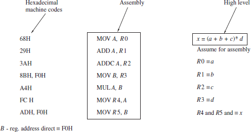
Figure 4.6 Exemplary nine machine codes, seven assembly codes and single high-level C language expression
Consider C langauge statement x = (a + b + c) × d. It implies the following:
- Take the number from address of b, add it in the number at address a.
- Take the number from address of c, add it in the number at address a.
- Take the number from address of d, multiply it in the number at address a.
- Put the result at the address of x.
Assembly language has seven instructions for the above statement; assume the following—the address of a is R0, address of b is R1, c is R2 and d is R3. It assumes the result x of 16 bits in R4 and R5. The operations by the instructions are as follows:
- Move R0 into A.
- Add R1 into A.
- Add R2 into A with carry generated in the previous addition operation
- Move R3 into B using direct address F0H for B.
- Multiply A and B (multiplication instruction is available for the multiplication of A and B not with A and R3).
- Move the lower byte as a result of multiplication in A into R4.
- Move the higher byte as a result of multiplication in A and B into R4 and R5. Use direct address F0H for B.
There are nine machine codes for the seven instructions in the assembly. We use the table in Appendix G for finding the machine codes for the instructions and SFR address F0H for B.
4.3 INSTRUCTION CYCLE
An instruction cycle is the cycle in which the steps take place for fetching an instruction (including fetching of needed operands) and for executing the instruction. Figure 4.7 shows an instruction cycle. It is measured in cycles. An instruction needs a minimum of one cycle. ADD A, R5 needs one cycle. ADD A, #08 also needs one cycle in 8051. MUL AB needs four cycles. A cycle takes 1μs period when XTAL frequency in MCU is 12 MHZ. This is because a cycle has six states, S1 to S6, and each state has two clock pulses (Fig. 3.7). MOVXA, DPTR is an instruction to move (transfer or copy) contents from the external memory address pointed by the DPTR 16 bits. It takes two cycles, each of six states.
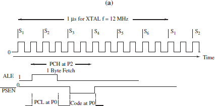
Figure 4.7 Timing diagram of instruction cycle for fetch operation in S1, S2 and S3 clock states if the length of the instruction is 1 byte
A timing diagram in Fig. 4.7 shows that if the length of instruction is 1 byte, it is fetched during S1, S2 and S3 states. Time is on horizontal axis. Logic state is on vertical axis. It shows at the bottom the durations for the PCL at P0 and code P0. Figure 4.8 shows that a 2-byte instruction is fetched during S1 to S6. Figure 4.9 shows that 3-byte instruction is fetched during nine states (first instruction cycle and half of second instruction cycle). The tables given in the following sections will also give the instruction lengths in bytes and the cycles to complete fetch and execute of each instruction.

Figure 4.8 Timing diagram of an instruction cycle for the fetch operation in S1 to S6 states if the length of an instruction is 2 bytes

Figure 4.9 Timing diagram of instruction cycles for the fetch operation in S1 to S6 clock states of the first instruction cycle and S1 to S3 of the second cycle if the length of the instruction is 3 bytes
4.4 EXECUTION TIME OF AN INSTRUCTION
Instruction cycle helps in estimating the time needed for executing an instruction. Adding the total number of instruction cycles in a program that will take during execution gives the total time required for the instruction.
For example, a two-cycle instruction will need 2 μs in 8051. This is because a one-cycle frequency is (1/12) fosc, where fosc is the XTAL oscillation frequency.
Example 4.7
Find the time taken in the following seven instructions. Assume 12 MHz Xtal with 8051. Use the number of cycles given in the tables for the instructions in Tables 4.1 and 4.8.
- MOV A, R0 takes 1 cycle (Table 4.1)
- ADD A, R1 takes 1 cycle (Table 4.8)
- ADDC A, R2 takes 1 cycle (Table 4.8)
- MOV B, R3 takes 2 cycles (Table 4.1) [It is MOV direct, Rn instruction where n = 3 and direct is the address 0F0H of B.]
- MUL A, B takes 4 cycles (Table 4.8)
- MOV R4, A takes 1 cycle (Table 4.1)
- MOV R5, B takes 2 cycles (Table 4.1)
Total number of cycles = 12 cycles. Time taken = 12 μs.
4.5 ADDRESSING MODES
An addressing mode is a method of specifying the data source or destination in an instruction. Figure 4.10 shows the various addressing modes. (Modes in dotted boxes are present in the other CPU families’ instructions.) The modes in the 8051 family instructions are as follows:
- Immediate: The data bits for instruction are a part of the instruction and are the next byte after the opcode.

Figure 4.10 Addressing modes (dotted box modes are the modes present in other CPU families)
For example, in ADD A, #08 the addressing mode is called the immediate addressing mode, because the source operand is the immediate (next succeeding) byte in the instruction. (Destination immediate addressing is not logical and hence not permitted.)
- Register: In this, the data bits for instruction are at a register(s). This is specified by the operand bits in the instruction. ADD A, R5 addressing mode is called the register-addressing mode, because the source operand is the register specified in the instruction.
- Direct: The address of 8-bits is directly specified in the instruction. Instructions for the SFRs have only the direct-addressing mode in 8051. Internal RAM between 0x00 and 0x7F is also accessible by direct addressing.
Example 4.9
For example, MOVR5, 90H (MOVR5, P1 for source at the SFR for P1 port. P1 has the address 90H).
Example 4.10
MOVR5, 0F0H (MOVR5, B. Source operand is SFR B. Direct address of B is 0F0H. A convention in assembly programs is to prefix 0 before a hexadecimal digit A or B or C or D or E or F so that the digit is not taken as a register).
Example 4.11
MOVR5, 3CH. Move the byte into R5 from internal RAM address 3CH.
The mode is called direct address mode because the source operand is from the address specified in the instruction.
Note:
- MOV R5, #90H will have a different mode. It moves the immediate operand into the R5. # sign specifies immediate operand as the source.
- Many direct addresses between 0x80 and 0xFF do not exist as there are much less than 128 SFRs.
- Indirect register (Indexed): The address (of 8-bits) is indirectly specified in the instruction by the contents of a pointer. Consider MOV A, R1. Here, MOV into A register the byte from the address pointed by the contents of R1. R1 and R2 are used as address pointers in 8051.
Example 4.12
Assume that R1 has byte 80H (pointer for Port P0 SFR address). MOV A, R1 transfers the byte from P0 using R1 as an indirect pointer for address. The addressing mode is so called because the source operand is from the address specified indirectly by another register in the instruction.
Example 4.13
8051 has a 16-bit register DPTR that works like a base register and points to an external memory address.
Example 4.14
68HC11 has two index registers, X and Y. Each one is of 16 bits. Either X or Y can be used along with an offset (displacement) bit defined in the instruction. Assume X points to a base address for the first rows first column of a table. X + Y can point to any row-first column addresses. The Y plus offset can point to any column in the row. Therefore, any table element address is X + Y + offset. Here, offset = displacement from the first column to the current column. Displacement is the address difference and is specified at the instruction.
Instructions for the internal RAM between 00H and 07FH have the indirect addressing mode also in 8051 in addition to the direct address mode. Instructions for the internal RAM between 80H and 0FFH have only the indirect addressing mode in 8052. (A convention in assembly programs is to prefix 0 before a hexadecimal digit A or B or C or D or E or F so that the digit is not taken as a register.) Internal RAM between 80H and 0FF (when present) is only accessible by indirect addressing.
Note:
- Direct addresses between 80H and 0FFH for the internal RAM area does not exist as there is SFR area at these addresses and SFRs are direct address accessible and therefore indirect address-specifying register must have the valid internal RAM address. For example, address 93H is valid in 8052 and invalid in 8051.
- Only R0 and R1 in a register bank are used in 8051 for indirect addressing.
- Bank for R0 or Bank for R1 depends on the RS0 and RS1 bits at the SFR PSW.
4.6 CLASSIFICATION OF THE INSTRUCTIONS AT THE INSTRUCTION SET
Instruction set of a CPU can be classified into the following. Figure 4.11 shows a classification of the instructions in the instruction set. (Appendix G gives the 8051 instruction set.)
It is as follows:
- Data Transfer Instructions
- Boolean Variable Manipulation Instructions
- Arithmetic Instructions
- Logic Instructions
- Program Flow Control (Processor and Machine Control) Instructions
- Interrupt Flow Control Instructions
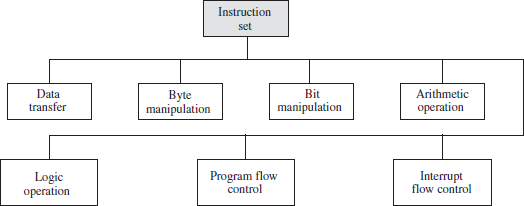
Figure 4.11 Classification of the instructions in the instruction set
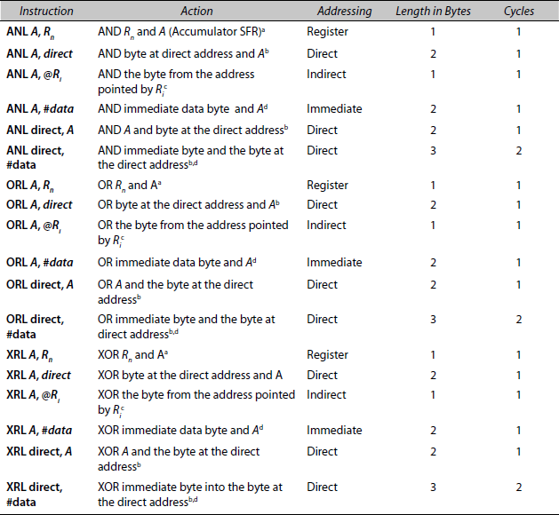
4.7 DATA TRANSFER INSTRUCTIONS
The 8051 instruction set has three types of the data transfer by move instructions. Transfer within the internal RAM and SFRs is of one type. The second type is transfer using code memory area (CODE and CONST). The third is using the external data memory (X-DATA). Figures 4.12(a)–(c) show the sequences in operations for data transfer instruction when using MOV, MOVC and MOVX instructions, respectively.
4.7.1 MOV Instructions
A MOV instruction means move (copy) the bits from one source to a destination. The 8051 MOV instructions are given in Table 4.1.
Table 4.1 MOV instructions within the registers, internal RAM and SFRs in 8051

a n is 0 or 1 or … or 6 or 7 for a register in the register bank. The bank is defined by RS0 and RS1 bits at PSW.
b Data bits of the byte to be moved.
c Direct is the byte for the address from where the byte at that address is to be moved. The address should be valid (existing SFR) in the SFR area or should be between 0x00 and 007F.
d i = 0 or 1. Byte to be moved from the address pointed by the contents of Ri. Prefix @ implies a pointer register. R0 or R1 can be a pointer register in a bank. The bank is defined by the bits RS0 and RS1 at PSW.
e Data of 16-bits to be moved into the DPTR. The DPTR is in two SFRs at the addresses 83H for DPL and 84H for DPH. Two direct addressing instructions will be needed if both are independently written.
One of the most important uses of MOV instructions are programming of the SFRs. Some examples are MOV into (i) TMOD and TCON for timer, or (ii) SCON for the serial interface device, or (iii) setting the interrupt masks in IE or (iv) set interrupt servicing priorities in IP. The second most important advantage is reading (moving) into a register the SFR SBUF serial input bits or moving the bits at the port into specified register (Rn) or reading internal RAM.
Example 4.15
Write the control bits 0100 0000 (40H) into the TCON.
TCON is an SFR. and it is in the direct-addressable space. TCON address is 88H. Instruction MOV direct, #data is there in Table 4.1. Using that the MOV TCON, #40H will be the instruction to write into the TCON.
Example 4.16
Load the external memory address pointer DPTR with 0x1000 (1000H). There is an instruction MOV DPTR, #data16 (Table 4.1). The instruction is, therefore, MOV DPTR, 1000H.
Example 4.17
Load 0x1000 (1000H) in DPTR. Write instructions using the DPL and DPH as the 8-bit operands.
Alternatively for the instruction MOV DPTR, #0x1000 we can use the fact that DPH and DPL are the SFRs at addresses 83H and 82H, respectively. There is MOV direct, #data instruction (Table 4.1). Instructions are as follows:
MOVDPH, #10H and MOVDPL, #00H or MOV83H, #10H and MOV82H, #00H.
Figure 4.12(a) shows three steps for instruction MOV @R1, A. This is an indirect addressing mode instruction. First step: R1 is read by the processing unit. Second step: pointed address 30H is found from R1. Third step: A is read and its contents found = 40H and 40H is transferred (copied) to address 30H from A.
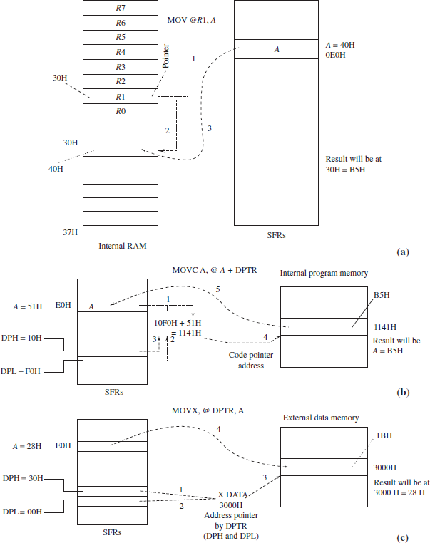
Figure 4.12 (a) Three steps for MOV @R1, A. The 40H moves to address 30H, which is pointed by Ri (b) using MOVC the B5H moves from 1141H into A (c) MOVX instructions the 28H moves into X-Data memory address 3000H
How can a byte be transferred from the address pointed by R0 to the register R2? There is no MOV @ Ri, Rn instruction available.
MOV @Ri, Rn is not an instruction present in 8051 but MOV Rn, A and MOV A, @Ri are available (Table 4.1). Hence, the byte pointed by R0 can first be moved into A and then to R2. The instructions are as follows:
MOV A, R0 and MOVR2, A to transfer a byte from the address pointed by R0 to the R2.
4.7.2 MOVC-type Instructions
An MOVC instruction means move (copy) the 8-bit code from one source at the program memory (internal or external) to the register A destination.
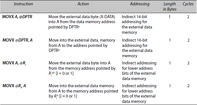
Figure 4.12(b) shows four steps for instruction MOVCA, @A + DPTR. This is an indirect addressing mode instruction. First step: 51H at A is read by the processing unit. Second step: pointed address lower byte DPL and higher byte DPH are read. Third step: DPH-DPL 16 bits 10F0H and 51H are added. The result 1141H is used as a pointer in the next step. Fourth step: 0B5H at the program memory address 1141H is transferred (copied) into A. A now has 0B5H.
The 8051 MOVC instructions are given in Table 4.2. These instructions are particularly important for accessing the constants (Table 2.2) in the program memory.
Table 4.2 MOVC instructions for transfer from the program memory area address code or constant to the accumulator in 8051

a DPTR does not change and is the base address. Address is relative to DPTR with index (offset) at A.
b PC does not change and is the base address. Address is relative to PC with index (offset) at A.
Another use of instruction MOVC is that it can be used to copy the codes from one set of memory area to another during the development phase. After the development phase is over, in certain 8051 MCUs there is a provision to disable its use by a security bit so that the internal program memory area cannot be copied later.
Example 4.19
Assuming PC to be 1000H, transfer the code at 1000H to the internal RAM at 70H.
For transferring the codes, the MOVC A, @A + PC is there in Table 4.2. First, we load A with 00H (Table 4.1). Then, we use the MOVC instruction to first get the code into A. From A, we can load it into adderss 70H.
(i) MOV A, #00H; (ii) MOVC A, @A+PC; (iii) MOV 70H, A; to read the code at 1000H into 70H.
Using DPTR, transfer the codes from 1000H and 1001H to addresses 7EH and 7FH in RAM.
For transferring the codes, the MOVCA, @ A + DPTR is there in Table 4.2. First, we load DPTR with 1000H and A with 00H (Table 4.1). Then, we use the MOVC instruction to first get the code into A, from where we load it into 7EH.
(i) MOV DPTR, 1000H; (ii) MOV A, #00H; (iii) MOVC A, @A + DPTR; (iv) MOV 7EH, A; to read the code at 1000H into address 7EH.
With DPTR already loaded, move 01H into A and use MOVC instruction again and move A to 7FH: (v) MOV A, #01H; (vi) MOVC A, A + DPTR and (vii) MOV 7FH, A ; to read the code at 1001H into 7FH.
4.7.3 MOVX-type Instructions
A MOVX instruction means move (copy) the 8-bit data into A and from A using the external data memory addresses using DPTR or Ri as the pointer.
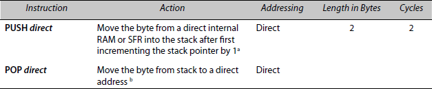
Figure 4.12(c) shows four steps for instruction MOVX @DPTR, A. This is an indirect addressing mode instruction. First step: Pointed address lower byte DPL is read. It is 00H. Second step: Pointed address higher byte DPH is read. Third step: DPTR points to address 3000H. Fourth step: 28H at A is transferred (copied) into data memory at address 3000H. Data memory 3000H address now has 28H.
The 8051 MOVX instructions are listed in Table 4.3.
The advantage of a separate MOVX is that it can be used to copy the bytes from or to using the external RAM for the data memory for X-DATA between 0000H and FFFFH.
Example 4.21
Using DPTR, transfer the codes from 1000H and 1001H to external data memory addresses 1000H − 1001H to show how we copy the codes from code memory in ROM to the external RAM.
For transferring the codes into A, the MOVC A, @A + DPTR is available (Table 4.2) and for the from A to external data memory, the MOVX @DPTR, A is available (Table 4.3). First, we load DPTR with 1000H and A with 00H (Table 4.1). Then, we use the MOVC instruction to first get the code into A.
(i) MOV @DPTR, 1000H; (ii) MOV A, #00H; (iii) MOVC A, @A + DPTR; to read the code at 1000H into A. DPTR is already loaded. From A, we can store the byte into external data memory at 1000H because DPTR = 1000H and we can use MOVX @DPTR, A. Therefore instruction (iv) MOVX DPTR, A is used.
Now, for saving the next code at the next address, we can perform the operations as follows:
(v) MOV DPTR, 1001H; MOV A, #00H; (vi) MOVC A, @A + DPTR and (vii) MOVX @DPTR, A; to read the code at 1001H and write into XDATA data memory 1001H.
Table 4.3 MOVX instructions for the transfer of 8-bit data into A and from A using the external data memory addresses using DPTR or Ri as the pointer in 8051
a DPTR (DPH and DPL together) has the 16-bit address for the external memory.
b Indirect 8 lower bits address for the external data memory defined at Ri. Upper bits are taken as 00000000b. Therefore, when the X-DATA memory address is between 0000H and 00FFH, the R0 and R1 can be used.
4.7.4 PUSH and POP Instructions for Using the Stack Area Employing the SP
PUSH instruction means move (copy) the 8-bit data into the stack after incrementing SP. The data are at a direct address. The address is of either an SFR or internal RAM between 00H and 7FH. Table 4.4 lists 8051 PUSH and POP instructions.
Table 4.4 PUSH and POP Instructions in 8051
a Stack pointer SP in 8051 is of 8 bits. 8051 Push instruction first increments the SP and then pushes the byte.
b Pop instruction pops the byte and then decrements the SP. Therefore, the initial value is always kept low, for example, 0x07, in place of 0xFF. (Default SP at startup is also 07H.) However, there is internal RAM and stack area overlap. We can set the initial value of SP as 7FH in the 8052 family, the PUSH will be only in the indirectly accessible area between 80H and 0FFH starting. Push is then at 80H and above. Therefore, the POPs will also the restricted to this area between 80H and 0FFH.
The advantage of the PUSH instruction is that the values in the registers, RAM or SFRs can be saved for the LIFO operations later. Some array values can be dumped on the stack and can be retrieved later as LIFO. For example, when we are arranging the values in the ascending order or in descending order.
Another advantage is that a variable of 1 byte can be saved at the stack temporarily by a PUSH.
An accumulator is used in a number of instructions. How will we save the value of A and retrieve when needed?
Table 4.4 shows that only PUSH direct instruction is available. We use PUSH 0E0H. A’s direct address is 0xE0.
Use of Stack to Save the Accumulator and Processor Status Word
Example 4.23
When using an ISR sometimes, there is need to save A and PSW on the stack. This is to make A and PSW available for use in the ISR. Before the last instruction return from the ISR, there is need to get the saved A and PSW back.
A register direct address is 0xE0 (=E0H). PSW register direct address is 0x0D0 (=D0H). We use PUSH 0E0H and PUSH 0D0H. We simply use PUSH A and PUSH PSW in case we are using an assembler, which will automatically place the direct addresses of A and PSW in the codes.
Note that we are using the default value SP here. Else, we can initialize SP by using MOV SP, #data or MOV81H, #data because 81H is direct address of SP.
Now, when needed, the stack-saved value can be retrieved by POP PSW and POP A.
Use of Stack to Save Registers at a Bank
Example 4.24
Assume that R0 to R7 have the array values in the ascending order. Assume register bank 0 is used. Rearrange these in the descending order.
We can use the LIFO property of the push and pop stack operations as follows:
(i) PUSH 00H; instruction to save R0 (note that PUSH R0 is not an instruction); (ii) PUSH 01H; (iii) PUSH 02H; (iv) PUSH 03H; (v) PUSH 04H and (vi) PUSH 05H; (vii) PUSH 06H; (viii) PUSH 07H; (ix) POP 00H; (x) POP 01H; (xi) POP 02H; (xii) POP 03H; (xiii) POP 04H; (xiv) POP 05H; (xv) POP 06H; (xvi) POP 07H;
Use of Stack to Save A and SP
Example 4.25
(i) Write 00H at Port P0, P1, P2 and P3 using POP instructions and using MOV A, #00H and PUSH 0E0H (equivalent to PUSH A). There should not be any effect on A and SP at the end of the instructions. (Use default SP of 07H.) (ii) How will we check that the SP remains unchanged at the end of a set of the instructions in a program?
First, let us save A and SP. (i) PUSH 0E0H (ii) PUSH 81H (equivalent to PUSH SP as the SP direct address is 81H); now, use MOV immediate, push and pop instructions to write into P0, P1, P2 and P3. (iii) MOV A, #00H; (iv) PUSH 0E0H; (v) POP 80H(equivalent to POP P1); (vi) PUSH0E0H; (vii) POP 90H (for popping into P1); (viii) PUSH 0E0H; (x) POP 0A0H(for popping into P2); (xi) PUSH 0E0H; (xii) POP 0B0H (for popping into P3). Restore SP first as it was pushed after A in instruction and restore A later; (xiii) POP 81H (equivalent to POP SP) and (xiv) POP 0E0H (equivalent to POP A) instructions first restore SP and then A from the stack.
We also check whether the SP does not change at the end of a set of instructions. We must count the number of pushes and pops. Both should be equal. In the above coding, note that both are equal.
4.7.5 XCH-type Instructions
An XCH instruction is for exchanging the A register with a source using the register (direct or indirect addressing) mode. An XCHD instruction is to exchange the lower hex-digit (nibbles) between the A and RAM using indirect addressing. The 8051 XCH and XCHD instructions are as per Table 4.3.
Table 4.5 XCH and XCHD instructions in 8051

a i = 0 or 1 for a register at a register bank.
b n = 0 or 1 or … or 6 or 7 at a register in register bank.
c If A has 50H and Ri has 7FH and at address 7FH the byte is 42H, then, A will have 42H and at address 7FH the byte will be 50H after the exchange.
The advantage of this XCH instruction is that the accumulator can be temporarily saved at an address and the value used from that address for arithmetic or logical operations. Later, the old value of A can be retrieved and the result after the operation will be back to that address by repeating the exchange instruction. Similarly, the lower digits can be operated and upper digits can be kept intact using the XCHD. For example, in TMOD, the lower digit is for the timer T0. Note that TMOD has to be first taken to the internal RAM address before being used for XCHD since its operand is accessible in the indirect addressing mode only.
Example 4.26
Swap the contents (bytes) at P0 and P1.
Table 4.5 shows that the exchange instructions between the bytes at the direct addresses are not available in 8051. However, XCH A, direct is available. Therefore, the following instructions will swap P0 and P1:
- XCH A, P0 (exchange A and P0 contents).
- XCH A, P1 (when exchanging A and P1 contents, P1 gets contents of original value of P0 through the A. Then, A gets the contents of P1).
- XCH A, P0 (when exchanging A and P0 contents, P0 gets contents of original contents of P1. A gets the contents of P0, which has A’s original value after the first instruction).
4.8 DATA AND BIT-MANIPULATION INSTRUCTIONS
4.8.1 Data Byte Manipulate (Clear, Complement, Rotate and Swap) Instructions
Figure 4.13(a) shows the byte manipulation instructions. These are for clear, complement, rotate and swap A. The source and destination operand addresses are the same and it is only the A (accumulator) that can be manipulated in 8051.
- A CLR instruction makes all bits 0s. A=0000 0000 after CLR A.
- A CPL instruction complements all 1s to 0s and vice versa. For example, if A=A5H=10100101 then after CPL the A=01011010b.
- An RL instruction rotates left. For example, bits 10001010b become 00010101b, and the C flag of PSW also becomes 1 after rotate left.
- An RLC instruction rotates left through the carry flag. For example, consider bits, A=10001010b and C=0. RLC makes A=00010100b and the C flag also becomes 1. After the rotate left through carry the C flag shifts to lsb (least significant bit) at A and msb (maximum significance bit) to C.
- RR and RRC are similar to RL and RLC instructions and are for the rotate right and rotate right through carry.
- RR rotates right and thus shifts lsb to msb and also to C.
- The C flag shifts to msb and the lsb to C in RRC after rotation.

Figure 4.13 (a) Operations in the byte manipulation instructions using A and (b) operations in the Boolean variable manipulation (bit manipulation) instruction using C or a bit at an address of the bit.
- SWAP is for swapping between the upper hex-digit with the lower hex-digit. For example, 89H will become 98H after SWAP.
- The 8051 CLR, CPL RL, RLC, RR, RRC and SWAP instruction features are given in Table 4.6.
Table 4.6 CLR, CPL RL, RLC, RR, RRC and SWAP instructions in 8051

Example 4.27
How do the mode bits of timers 0 and 1 swapped at the TMOD?
TMOD has the lower nibble for the mode of timer 0. TMOD upper nibble is for timer 1 mode. Table 4.6 shows that instruction for swap of nibbles is available for swap in A only.
The following instructions will swap the lower and upper nibbles of modes of timers 0 and 1.
- PUSH 0E0H (for saving A onto the stack).
- MOV A, 89H (equivalent to MOV A, TMOD as 89H is the TMOD direct address).
- SWAP A.
- MOV89H, A.
- POP 0E0H (for restoring the A from the stack).
Example 4.28
What will be the effect of RRC A, assuming A = 02H and C = 1?
The RRC instruction means rotate right through carry. Original carry will move to msb and original lsb into CY. Therefore, C will become 0 as 02H = 0000 0010b in A. The result will be 1000 0001b in A. Therefore, A will now be 81H.
Example 4.29
What will now be the effect of CPL A? Assume that it executes after the RRC in Example 4.28.
The CPL A instruction means complement A. A = 81H at the beginning after the RRC. Therefore, A will become 0111 1110 (7EH) after CPL A.
Complement the port P2 bits.
The 8051 has all the arithmetic and logic operations using the A (accumulator). Table 4.6 shows that there is no complement direct instruction. Port P2 bits can be complemented though the use of A. The instructions will be as follows:
(i) XCH A, P2; (ii) CPL A and (iii) XCH A, P2.
Note that the combination of two instructions (i) and (iii) restores A to the original value. One can also use (i) MOV A, P2; (ii) CPL A and (iii) MOV P2, A. However, this will affect the contents of A.
Example 4.31
How can the bits be rotated using the rotate instruction without affecting C at the end?
Use PUSH 0D0H (equivalent to PUSH PSW) at the start of the rotate instruction and POP PSW at the end.
4.8.2 Boolean Variable (Bit) Manipulate and Boolean Processing Instructions
Figure 4.13(b) shows the bit-manipulation instructions. These are also called Boolean processing instructions. The source or destination operand is either C or bit. The C or bit is clear, set, complement. There can be transfer (copy) or ANDing and ORing using bit and C. C acts like the Boolean accumulator like the A in byte-manipulating instructions.
The bit means bit at a bit address. Refer Table 3.2 for the bit addresses (between the 80H and FFH in select SFRs like P0, P1, …). Refer Figure 3.6 for the bit addresses between 00H and 7FH for 16 bytes at the internal RAM between 20H and 2FH.
- A MOV instruction transfers the bit between C and bit.
- A CLR instruction makes C or bit = 0.
- A CPL instruction complements C or bit. For example, the bit at bit address 93H will be 0, if 1. Note that 93H is for the bit 3 in byte at P1 (Table 3.2).
- A SETB instruction sets C or bit. For example, the bit at bit address BAH = 1b after the SETB. Note that BAH is the address of bit 2 in SFR IP (Table 3.19).
- An ANL instruction does ANDing between C and bit or complement of the bit,
 . For example, assume bit at P2 bit 3 (address = B3H) = 1 and C = 0. After ANDing C and bit P2.3, C becomes 0.
 - An ORL instruction does ORing between C and bit or complement of the bit, . For example, consider bit at RS0 = 0b (address D3H). It is a PSW bit. And C=0. After ORing C and bit PSW.3, C becomes 1.
The 8051 MOV, CLR, CPL, SETB, ANL and ORL instruction features are given in Table 4.7. These are the important instructions for setting or clearing the bits, like for the ports, TCON, SCON, A, B, PSW, IP and IF.
Example 4.32
Write instructions (i) P1 port bit 0 = 0, (ii) IE bit 7 = 1 and (iii) Complement TCON bit 6.
We use Table 4.7 instructions for clearing, setting and complementing the bits as follows:
- CLR P1.0 or CLR 90H to clear the bit at the bit address 90H,which is P1.0.
- SETB IE.7 or SETB 0AFH to set the bit at the bit address AFH, which is IE.7.
- CPL TCON.6 or CPL 08EH to complement the bit at the bit address 8EH, which is TCON.6
- CPL 0BH to complement the bit at the bit address 0BH, which is bit 3 at 21H (remember 00H to 07H are the bit addresses for RAM at 20H and 08H to 0FH, the bit addresses for RAM at 21H).
Example 4.33
Complement the bit 3 of internal RAM at 21H.
CPL 0BH. It complements the bit at the bit address 0BH, which is bit 3 at 21H (remember 00H to 07H are the bit addresses for RAM at 20H and 08H to 0FH, the bit addresses for RAM at 21H).
Example 4.34
Move bit 2 of P3 into C.
Consider bit at P3 bit 2 (address B2H) 1 and C 0. After MOV C, 0B2H instruction, C becomes 1. [C is a Boolean processor accumulator.]
Example 4.35
Clear bit 1 at the RAM at 20H.
It means make 0 the bit at bit address 01H. Since 01H has the bit 1 in the RAM byte at 20H, CLR 01H is the instruction.
Example 4.36
Start timer 0 by setting TR0 bit in TCON.
Address for the byte of TCON is 88H, and TR0 at it is bit addressable by the bit address 8CH (Table 3.11). Therefore, the instruction is SETB 8CH to make TR0 = 1.
Table 4.7 MOV, CLR, CPL, SETB, ANL and ORL Boolean processing instructions in 8051

a These operations do not affect the flags unless the destination address bit is at PSW (between D0H and D7H).
Example 4.37
Test whether Port P2 bit 5 is set (=1).
Address for the byte of P2 is A0H, and bit 5 at it is bit addressable by the bit address A5H (Table 3.2). Therefore, the instructions are as follows:
SETB C; ANL C, A5H; if C becomes 1 when instruction executes, then P2.5 is 1, else it is 0.
4.9 ARITHMETIC INSTRUCTIONS
Figure 4.14(a) shows the arithmetic instructions. The instructions are for 8-bit addition, subtraction, increment, decrement, multiply and division instructions. There is a 16-bit DPTR increment (without affecting the flags) instruction. Assume 12 MHz XTAL crystal with 8051, then an instruction cycle has 6 states S1 to S6 and each state has two clock pulses generated by the oscillator. Therefore the cycle time = 1 μs. Multiplication and division then take 4 μs and increment DPTR take 2 μs.
- Add and subtract and increment and decrement instructions. The instruction uses one of the four addressing modes each—register, immediate, direct and indirect.
- There are two sets of addition instructions—add without carry and add with carry. Both use one of the 4 models of addressing. Figure 4.14(b) shows five steps for ADDC A, R3. Step 1: Read C = 1. Step 2: Read 50H at A. Step 3: Read 81H at R3. Step 4: Add 50H, 1 and 81H and Step 5: Put the result D2H in A and since the result is no carry, no auxiliary carry and no overflow, clear the C, AC and OV in PSW.
- There is only one set of subtract instruction—subtract with borrow (C). Subtract without borrow can be done in two steps—CLR C and then SBBB.
- C, OV and AC are affected as follows: C is set when the addition results in answer > FFH and set when subtraction results in the answer < 00H. AC is set when an addition or subtraction in the lower-nibble operation changes the value of the upper-nibble. AC is used for decimal adjusting the result by DA A instruction after the addition. OV is useful in addition or subtraction of the signed numbers.
- Multiplication and division instructions use only the register-addressing mode and use only A and B. OV is affected and is useful in determining whether 8 bits multiplied by 8 bits results in an 8 bit (when OV0) or in 16-bit (when OV 1) number. OV is also useful in determining that denominator was 0 earlier (OV = 1) or not (OV 0) during the division.
- DA A (decimal adjust accumulator) instruction use only the register addressing mode and uses the A.
- INC DPTR instruction has only one addressing mode—16-bit register (pair) addressing mode and uses DPL and DPH.

The 8051 arithmetic ADD, SUB, MUL, DIV, INC and DEC instruction features are given in Table 4.8.

a n is 0 or 1 or … or 6 or 7 for a register in the register bank defined by RS0 and RS1 of PSW SFR.
b OV 1 if there is a carry out of the bit position 6 but not from bit position 7 or if there is a carry out of bit position 7, but not from bit position 6 during subtraction. OV is thus an exclusive OR operation between the carries from bit 6 position and bit 7 position. When OV 1 and C 0, it means that the result becomes above 128 but is below 256. When OV 0 and C 1, it means that the result becomes above 256 with carry from bit position 6 as well as 7. When OV 1 and C 1, it means that the result becomes above 256 with no carry from bit position 6 but carry bit from position 7. Remember that in two’s complement arithmetic, a byte above 127 means overflow in subtraction. (255 means FFH. 256 makes A 0.)
c Direct is the byte for the address from where the byte is to be used in arithmetic operation. Address should be valid (existing SFR) in the SFR area or should be between internal RAM 00H and 7FH. d i = 0 or 1 the byte to be moved from the address pointed by the contents of R.. Prefix implies a pointer register. R0 or R1 is a pointer at a register in a bank. The bank defines by the bits RS0 and RS1 in PSW. e Data mean the byte to be used in arithmetic operation.
f LSB means least significant byte and MSB means maximum significant byte.
g OV sets if the result of multiplication exceeds FFH and higher bits b8-b15 of the result are at B. C always resets to 0.
h Unsigned numbers division, when the radix points of numerator and denominator at the same bit position, OV and C both reset to 0s. The OV sets to 1 when the resulting quotient and remainder are indeterminate (remain undefined in the case when the denominator happens to be zero). In the quotient, the radix point is to the right side of lsb (bit-0) in A. C always resets to 0.
Example 4.38
Add 128 and 129 decimals.
The 128 decimal means 80H and 129 means 81H. Table 4.8 shows that one of the bytes must be placed in A. 8051 ALU needs one of the operands at the accumulator. The instruction will therefore be as follows:
(i) MOV A, #80H (Refer Table 4.1). (ii) ADD A, #81H; the result in A will be 01H and carry will be 1 and OV 1. That means that the result is 256 decimal + 1 = 257 and both additions are of numbers of the same negative sign. The answer is taken as −257 because OV 1.
Example 4.39
Subtract decimal 129 from 128 and then subtract 5 again.
Subtract without borrow is not available in 8051 (Table 4.8). We should first clear carry and then subtract in the first time operation of subtraction of 128 and 129. C (borrow) is likely to generate in the first subtraction, hence in subsequent subtractions, we always use subtract with borrow. Instructions will be as follows:
(i) MOV A, #80H (move 128 decimal in A) [Table 4.1] (ii) CLR C (clear carry which is also for the borrow so that C, set in any previous operation, becomes clear now) (Table 4.7), (iii) SBBB A, #81H (Table 4.8). The result in A will be FFH and carry will be 1 and OV = 0 due to borrow at the 6th as well as the 7th position. This corresponds to −1. Both numbers were of the same negative sign and (iv) SBBB A, 05H (second subtraction). The result will be F9H and C resets to 0 and OV = 0. The result has to be adjusted because it means that both the numbers were of the opposite signs. Therefore, the adjusted result should be considered as −6 and not as −7.
Example 4.41 also shows how we can write assembly instructions in an appropriate format.
Example 4.40
Add 16-bit numbers at R0−R1 (lower byte at R0) with another 16-bit number at R2−R3 (lower byte at R2) and place the result at R4−R5 (lower byte at R4). Let us use the instruction starting at 00A0H. Use Appendix G to specify codes.
Carry flag is needed in the present program because 8-bit addition instructions ADD and ADDC affect C, AC and OV.
; Program Example 4.40
; Uses PSW.7 bit, PSW.6 and PSW.2 (C, AC and OV) and the 8-bit accumulator.
; Raj Kamal August 15, 2009
; Variables at R0 to R5,
; Temporary variables at R6 and R7
; org 0x0A0

4.10 INSTRUCTIONS FOR LOGICAL OPERATIONS ON BYTES AT THE REGISTERS, INTERNAL RAM AND SFRS
Figure 4.15 (a) shows the operations during the logic instructions. The AND, OR and XOR instructions have four addressing modes each — register, immediate, direct and indirect. When there is a 12-MHz XTAL with 8051, the instruction cycle equals one cycle. Each cycle has six states. One cycle period = 1 μs and is identical for the AND, OR and XOR instructions for register, direct and indirect addressing modes. It is 2 us when the immediate addressing mode for source 2 and the direct for source 1 are used.(Table 4.9)
The 8051 logic ANL, ORL and XRL (and, or and xor logic, respectively) instructions are given in Table 4.9. Figure 4.15(b) shows three steps in the implementation of ANL A, P2. P2 direct address is A0H. Step 1: Read 80H from A (address E 0H). Step 2: Read 08H from P2 (address A0H). Step 3: ALU does logical AND operation between the two. Write the result 00H into A.
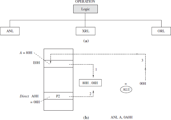
Figure 4.15 (a) Operations in the logic instructions and (b) three-step implementation of ANLA, A0H The operations are at addresses E0H and 08H.
Table 4.9 ANL, ORL and XRL instructions in 8051
a n is 0 or 1 or … or 6 or 7 for a register in the register bank defined by RS0 and RS1 of PSW SFR.
b Direct is the byte specifying the address from where the data byte is to be used in arithmetic operation. The address should be valid (existing SFR) in the SFR area or should be between 00H and 7FH RAM.
c i = 0 or 1, the byte to be moved from the address pointed by the contents of Ri. Prefix implies a pointer register. R0 or R1 is a pointer register in a bank. The bank is defined by the bits RS0 and RS1 in PSW.
d Data means the data8 immediate operand of 8 bits used in arithmetic operation.
Example 4.41
Let A = FFH. AND and A the bits at SBUF using an ALU instruction.
We can AND A and the SBUF by the AND operation of A with SBUF using ANL A, direct instruction in row 2 of Table 4.9 as SBUF has a direct address 99H. The instruction will be as follows:
(i) When A = FFH then the instruction to AND A and SBUF is as follows: ANL A,99H (Table 4.9). This is equivalent to ANL A, SBUF.
Example 4.42
Set the bits 7 and 6 at SCON without affecting other bits.
First, set the bits 7 and 6 and reset all the remaining bits in A by MOV A, #data (Table 4.1) and then perform the OR operation of A with SCON. The instructions are:
(i) ORL SCON, #C0H. All bit except the 6th and 7th = 0s.
Example 4.43
How can we start timers 0 and 1 at the same instance?
Refer Table 3.11; Timers 1 and 0 start when TR1= 1 and TR0 = 0. TR1 and TR0 are TCON 6th and 4th bits. TCON address is 88H. Instruction will be as follows:
(i) ORL 88H, #50H; after the instruction executes, bits at TCON are ORed with 01010000. All except the 6th and 4th bits = 0s (Table 4.1) 88H, A.
Example 4.44
How can we toggle the bits at Port 2? (Make P2 bits = 1s as 0s and 0s as 1s). Table 3.2 gives the Port 2 direct address is A0H. An XOR operation with 1 makes a bit 0 if previously 1 and makes it 1 if previously 0. Therefore, if P2 is XORed with = all 1s (= FFH) and then use of the XOR instruction for toggling bits.
(i) XRL P2, #0FFH toggles the bits at P2 at direct address A0H.
Example 4.45
Use ANL, ORL and XRL instructions for the bytes for clearing, setting and complementing the specific bits.
- TCON register bit 7 is to be cleared. TMOD bits are not addressable by the bit addresses.
Therefore the instruction is:
ANL TCON, #7FH; AND with 0111 1111b to clear bit 7 (msb)
- SCON register bit 0 is to be set. The instruction is:
SCON, #01H; OR with 0000 0001 to set bit 0 (lsb)
- A register bit 6 is to be complemented. The instruction is as follows:
XRL A, # 40H; XOR A with 0100 0000 to complement bit 6 (msb but1)
- R0 register bit 2 is to be complemented. There is no XRL instruction, which has R0 as destination The instructions are as follows:
- MOV A, R0; Move R0 into A to enable XOR operation between 2 bytes
- XRL A, #04H; XOR A with 0000 0100b to complement bit 2
- MOVR0, A; Move back changed into R0 from A.
4.11 PROGRAM-FLOW CONTROL INSTRUCTIONS
Program-flow instructions change the program flow from sequential order. The instructions for jump, call and reset instructions are called program flow instructions. They change the program counter to a value other than the one present after the increment of program counter just after an instruction fetch. A program may have the while or for loop. It may have the conditions for executing a specific section of the instructions. A program may jump to another address in case of executing a conditional instruction or while-loop or repeat loop. The program may call other routine(s) in between the instructions. The routine may return to calling routine or program at the end of the instructions. These actions warrant a change in the program-flow path. The program counter after steadily incrementing after each code of the instruction acquires a new value to start another program-flow path.
4.11.1 Delay-cycle (NOP) Instructions
The 8051 has NOP instruction. It means no operation, just spent one instruction cycle time.
a For a XTAL of frequency 12 MHz, the cycle consists of 1 us because 1 cycle has six states S1 to S6 and each state has two pulses.
Suppose a port pin connects to a driving transistor. The transistor drive the current in the speaker. We can program delays for sending 1s and 0s. The delay intervals depen on the musical note sent to the speaker. The musical notes are played successively in a song.
Example 4.46
How can we toggle the bits at Port 2 and again toggle after a delay of 10 μs? (Make the bits = 1s as 0s and 0s as 1s. Delay 10 μs. Again make 1s as 0s and 0s as 1s.)
Refer Example 4.44. Assume that XTAL oscillation frequency = 12 MHz. We introduce the delay of 10 us using 8 NOPs. Then repeat XOR operation with P2 after the NOPs. Instructions will be as follows:
(i) XRL 0A0H, #FFH (XRL with all bits = 1s) (equivalent to XRL P2, #11111111b as direct address of P2 is A0H) (ii) to NOP; NOP; NOP; NOP; NOP; NOP; NOP; NOP; (x) XRL P2, #FFH.
Eight NOPs for 10 μs because of one instruction cycle time each spent in NOP instructions and XRL P2 takes 2 cycles, there is a 10 instruction cycle time which is spent, thus there is delay of total next address 10 μs.
4.11.2 Long, Absolute and Short Jumps
The 8051 has three jump instructions—jump to any 16-bit address, jump to address within the 2 kB space and jump to the address within 128 bytes above or below the present address. These are called long, absolute and short jumps. Table 4.10 gives the jump instructions and the cycles taken for operations.
Table 4.10 Long, absolute and short jump instructions in 8051

a 16-bit address in long jump (LJMP)—Instruction Opcode bits = 8.
b Jump within the next 2 kB address space of the currently executed program (of program memory); the five highest significant bits are unchanged in the PC in absolute jump (AJMP). Instruction Opcode bits = 5.
c rel is a signed number and a signed 8-bit number has the decimal value between −128 and +127. Instruction Opcode bits = 8.
d 16-bit address is indirectly found. JMP-instruction Opcode bits are 8.
Figure 4.16 shows the operations for the—AJMP Addr11instruction. Figures 4.16 shows that 5 upper bits from PCH are the 5 msb in the 16-bit memory address. Three upper bits in the first byte of AJMP instruction are next 3 bits after 5 msb in 16-bit memory address. Eight bits in the second byte of AJMP instruction are 8 bits after 8 msb in the 16-bit memory address. It means the second byte of AJMP instruction transfers to lsb 8-bits in a new value of PC. (It also means that this byte transfers to PCL.)
Example 4.47
Jump to a program memory address after 8 kB addresses (2000H addresses) from the location of the next instruction, which is 1000H.
The jump is above 2 kB code space (Table 4.10). We can, therefore, use only the jump long. Now, 1000H + 2000H = 3000H. Therefore, the instruction is as follows: LJMP 3000H.
Example 4.48
Jump to a program memory address after 16 addresses backwards from the location of the next instruction, which is 1000H.
Jump is relative and is to less than 256 locations (Table 4.10). We can, therefore, use the jump short. Now −16 decimal = F0H. [Two’s complement number of 16d is FOH]. Therefore, instruction is as follows: (i) SJMP 0F0H.
Example 4.49
Jump to a program memory location after 16 locations backwards relative to the DPTR contents. Jump is relative and backward but using DPTR (Table 4.10). We can, therefore, use the JMP @A + DPTR. Now −16 decimal = F0H. Therefore, the instructions are as follows:
- MOV A, #0F0H
- JMP @A + DPTR
Example 4.50
Jump to a program memory address after 1000 locations from the beginning of current instruction. Jump is within the 2 kB code space (Table 4.10). We, can, therefore, use jump absolute. Since jump takes place not from the current but from the next instruction after the jump instruction and jump absolute instruction length = 2 bytes, jump has to be after 1022B. The 11 bits for 1022 decimal = 011 1111 1110. The 5-opcode bits are the lower bits opcode of AJMP is 00001 and 011 for the needed for higher bits. Therefore, the instructions will be as follows:

Figure 4.16 Operations during the jump instruction—AJMP Addr11
AJMP 0FEH; (with 1st byte = 61H and 2nd byte = FEH) (Table 4.10)
4.11.3 Conditional Short Relative Jumps
The 8051 has seven conditional jump instructions and these are given in Table 4.11. The table also gives the cycles taken during the operations of these control instructions.
Table 4.11 Conditional short relative-jump instructions in 8051

Note: rel is a signed number and a signed 8-bit number has the decimal value between −128 and +127. Instruction opcode bits = 8.
Example 4.51
If SCON.4 (serial receiver enable) = 1, then jump to a program memory location which is 32 locations back-wards from the location of next instruction. Next instruction is at 1040H. Reset carry also.
Refer Table 3.16. SCON.4 bit address = 9CH. Jump is relative and is within 256 locations. Refer Table 4.11. We can, therefore, use the conditional jump short. Now −32 decimal = E0H [Two’s complement number of 32 is E0H]. Therefore, the instruction is as follows:
(i) JBC 9CH, 0E0Hat the address 103DH. (Note: When assembling, we use 0E0H for E0H by convention).
Example 4.52
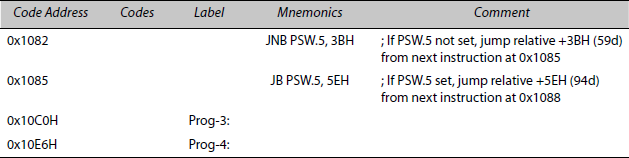
Execute program-3 instructions from memory location 0x10C0 if input at the user flag F0 = 0, else program-4 from 0x10E6. Let the present program addresses start from 1082H.
: Program Example 4.52
: Exemplary use of the JNB and PSW and F0 bits in the instructions
: Variable declaration—Boolean PSW.5 (F0 is at PSW.5)
: Org 1082H
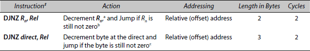
4.11.4 Decrement and Conditional Jump on Zero
The 8051 has two instructions for decrement the register and direct. There is conditional jump if the decrement does not result in all bits at register or direct address = 0s. These instructions are extremely valuable in case of the looping. There is exit from the loops after executing a certain number of loops. Table 4.12 gives the instructions. The table also gives the cycles taken for the operations of the instructions.
Table 4.12 Instruction for decrement and then jump in program loops in 8051
a n is 0 or 1 or … or 6 or 7 for a register in the register bank defined by RS0 and RS1 of PSW.
b Example is MOV R1, #FAH; DJNZ R1, −2; This means loop back 250 times and takes 500 cycles, two cycles for each DJNZ execution. 1 cycle takes 1 μs if 12MHZ XTAL is used. 2 cycles takes 2 μs. 500 cycles takes 500 μs. Total delay is 500 μs.
c Direct is the byte at the address from where the byte is to be moved. Address should be valid (existing SFR) in the SFR area or should be between 0x00 and 007F.
Note: relis a signed number and signed 8-bit number has the decimal value between −128 and +127.
Example 4.53
A wait loop (delay loop) example is NOP containing loop. Consider following instructions:
MOV RI, #FA; NOP; DJNZ RI, −3;
We use rel = −3 (equivalent to FDH) in the above instruction as DJNZ R1, Rel instruction is 2 bytes long and thus the program counter increments to +2 on executing a DJNZ instruction. Decreasing the PC by 3 brings PC back to the start of the NOP instruction before the DJNZ instruction. A wait loop sets by DJNZ RI, −3 with R1 decrementing by 1 on every looping once. Looping is till R1 continues to be not 0.
Loop will execute 250 times because R1 = 250 after MOV R1, #FA and the time taken will be 250 (1 + 2) μs when the delay loop is using DJNZ instruction as it takes 2 cycles of 2 μs and NOP takes one cycle of 1 μs. Time taken in one loop = 3 μs. Delay = 750 us within the loop.
Example 4.54
MOVR1, #FA; NOP; NOP; DJNZR1, −4; instruction will delay by 1000 ms.
We use rel = −4 (equivalent to FCH) in the above instruction as DJNZ R1, Rel instruction is 2 bytes long and thus the program counter increments to +2 on executing a DJNZ instruction. Decreasing the PC by 4 brings PC back to the start of the first NOP instruction after MOV instruction. A wait loop sets by DJNZR1, −4 with R1 decrementing by 1 on every looping once. Looping is till R1 continues to be not 0.
Loop will execute 250 times because R1 = 250 afterMOVR1, #FA and time taken will be 250 (1 + 1 + 2) μs when the delay loop is using DJNZ instruction as it takes 2 cycles of 2 μs and two NOPs within the loop takes one cycle each of 1 μs. Time taken in one loop = 4 μs. Delay = 1000 us within the loop.
Use of a Loop within a Loop
Example 4.55 demonstrates how one can use a loop within a loop.
Example 4.55
How can we toggle bits at Port 2 after a delay of 4007 μs? Make the bits which are 1s as 0s and 0s as 1s.
Assume that XTAL oscillation frequency = 12 MHz. Refer to Example 4.44 for use of XRL for complementing the port bits. Refer to Example 4.54 for the use of DJNZ for delay using 1 loop. We introduce the delay of 4000 us by using delay program, which uses a DJNZ instruction. Repeat the XOR operation with P2. Instructions will be as follows:
- MOV A, #FFH; (make all bits of A = 1s). [Cycle Time = 1μs.]
- MOVR0, 04H. Now delay 1000 μs by the next loop instruction.
- MOVR1, #FAH; NOP; NOP; DJNZ R1, −4 (instruction loop will delay by 1000 μs.
- DJNZ R0, −7 (instruction will delay four times of 1001 μs).
- XRL A, P2 (make each bit of P2 = 1 if 0, and 0 if 1). [Cycle/Time = 1 μs ]
- MOVP2, A. [Cycle/Time = 1 μs.]
Total time taken in steps (i) to (vi) = 4007 μs.
Note: Use 0 prefix before A, B, C, D, E or F first hex-digit when using hex-digits. It is a conventional usage in an assembler.
Example 4.56 shows the use of DJNZ in transferring a 32-byte block of memory from 40H to 60H by using R0 and R1 as the index registers and INC instruction.
Example 4.56
There is a 32-byte block of memory from 40H. Transfer it to the block from 60H.

4.11.5 Jump After Comparison
The 8051 has four instructions for compare and then conditional jump after comparison. These are given in Table 4.13. The table also gives the cycles taken for the operations of the program-flow control instructions.
Table 4.13 Compare and then conditional jump after comparison in 8051

Note: rel is a signed number and a signed 8-bit number has the decimal value between −128 and +127. Addressing in column 3 is for jump operation.
a C=1 if A or Rn or byte pointed by Ri is not equal to the compared source operand. The compared operand is direct or immediate byte and that is less than the source operand.
b n is 0 or 1 or … or 6 or 7 for a register in the register bank defined by RS0 and RS1 of PSW.
c Direct is the byte for the address from where the byte is to be moved. Address should be valid (existing SFR) in the SFR area or should be between 0x00 and 007F.
d Indirect 8 bit address for the internal data memory defined by contents of R.. Memory address is between 00H and 7FH. The i = 0 or 1. Therefore, R0 and R1 are used at a register bank. [Between 00H and FFH in 8052]
4.11.6 Call to a Routine and Return from Routine
The 8051 has two call instructions—call to any 16-bit address and call to address within the 2 kB. These are useful for the call long and absolute to a routine. Table 4.14 also gives the instructions and cycles taken for the operations in instructions. Figure 4.17 shows the operations in LCALL.
8051 CPU saves on a call only the PC (PCH and PCL) onto the stack. SFRs, which are expected to be changed on calling the routine must be saved by push and must be popped before the last return instruction at the routine. It shows that PCL and PCH of the next instruction in presently running program saves at the stack top in two pushes of PCL and PCH. It shows that 8 msb bits at PCH are taken from the third byte of the LCALL addr16 instruction. It shows that 8 lsb bits at PCL are taken from the second byte of the LCALL addr16 instruction.

Figure 4.18 shows the steps for operations needed on RET instruction for return from a routine. Assume that before calling this routine SP = 30H and return address 20F0H. Step 1: Pop PCH from stack top at 32H and decrement SP. Step 2: PCH gets new bits = 20H. Step 3: Pop PCL from the stack top now at 31H and decrement SP. PCL = F0H. Step 4: SP at 81H gets the bits the same as the ones before calling the routine. SP = 30H on return.
Table 4.14 Long, absolute call and return instructions in 8051

a 16-bit address in long call (LCALL)—Instruction opcode bits length = 8, 16-bit address in PCL and PCH of the next instruction saves on the stack. For saving PCH and PCL, each time (SP) increments by 1.
b Call within the 2 kB address space of the currently executed program; the 5 highest significance bits are unchanged in the PC; called Absolute Call (AJMP). Instruction opcode bits = 5.
c Return after retrieving PCL and PCH into the PC, which were previously saved onto the stack. The calling program starts on return.
Example 4.57
Call to a program memory address after 3 kB locations (after 0C00 addresses) from the address of the next instruction, which is at 1000H.
Call is above the 2kB code space (Table 4.14). We can, therefore, use only the call long. Now, 1000H + 0C00H = 1C00H. Therefore, the instruction is as follows: (i) LCALL 1C00H (Table 4.14).

Example 4.58
Call to a program memory location after 1026 kB locations from the current call instruction at 00F0H. Where will be PC on return from the called routine? What will be the bytes at stack top after the call?
Call is within the 2 kB code space (Table 4.14). We can, therefore, use call absolute. Hence, ACALL can be used. Call takes place not from the current but from the next instruction after the call instruction and call absolute instruction length = 2 bytes. Hence, call has to be after 1024 addresses from 00F2H = 0000 1111 0010b. The 11 bits for 1024 decimal are ![]() 0000 0000 and these are added with 0000 0000 1111 0010b = 0 0
0000 0000 and these are added with 0000 0000 1111 0010b = 0 0![]() 1111 0010b. Upper 5 msb are the same as the 5 msb of the program counter of current instruction.
1111 0010b. Upper 5 msb are the same as the 5 msb of the program counter of current instruction.
5-opcode bits are the lower bits opcode of ACALL, which is 1 0001 and ![]() are the higher bits in the above calculation. Therefore, the instruction for call is as follows:
are the higher bits in the above calculation. Therefore, the instruction for call is as follows:
(i) ACALL F2H (with 1st byte = ![]() 1 0001 = 91H and 2nd byte = F2H) (Table 4.14).
1 0001 = 91H and 2nd byte = F2H) (Table 4.14).
Program counter on return from the routine has to be at 00F2H. Therefore byte at the stack top should be F2H and the byte at the stack top −1 should be 00H.
4.12 INTERRUPT CONTROL FLOW (RETI INSTRUCTION)
Figure 4.19 shows the return steps from an interrupt service routine. 8051 CPU saves on an interrupt only the PC (PCH and PCL) onto the stack before start of execution of an interrupt service routine. SFRs, which are expected to be changed at the routine, must be saved by push and must be popped before the last return instruction at the routine.
The 8051 has a return from interrupt instruction as follows:
a Return after retrieving PCL and PCH into the PC, which were earlier saved onto the stack and transfer t he program control to the next priority interrupt if that is pending for the service and if that is not masked.

4.13 ASCII-RELATED APPLICATION PROGRAM
Example 4.59 shows an ASCII code conversion-related application. It uses the table of ASCII codes for the numbers between 0 and 9. It shows creating of a new array of ASCII codes. The codes rearrange as per the sequence of 10 characters which were input from a telephone dialing keypad. The example shows the use of R0, R1, R3 and R4 as the GPRs (general purpose registers). R4 is used for count. R3 is used as a base address. R0 is used as base and index pointer and R1 as the index pointer.
Example 4.59
Let the keys pressed for a telephone number be 9, 8, 9, 1, 5, 7, 0, 0, 3, 3. When the key 8 is pressed then P1 gets the input 00001000b. The corresponding array of ASCII codes is required to be 39H, 38H, 39H, 31H, 35H, 37H, 30H, 30H, 33H and 33H. Let the 10 ASCII codes (30H to 39H for digits 0 to 9) for the 10 digits be stored at a table in the internal RAM between 70H and 7AH in 8051. When the telephone number digit is input at P1, the following instructions will retrieve the appropriate ASCII code from the table and save the 10 digits sequentially in ASCII code array form between internal RAM 40H and 49H according to the dialled numbers.
| Label | Mnemonics | Comment |
|---|---|---|
Init: |
MOV R3, #70H |
; Load R3 with the starting base address of the table of ASCII codes |
|
|
; R1 points to the ASCII coded array, which is to be created |
|
MOV R1, #40H |
; Count = 10 for total number of phone digits in R4 |
|
MOV R4, #0AH |
|
MOV A, P1 |
; Load A with P1 with the digit at P1 (= R3) |
|
|
ADD A, R3 |
; Find in A address of the code by the addition of base address |
|
MOV R0, A |
; Move the address in R0 because R0 is to be used as address |
|
|
; pointer for the code |
|
MOV A, @R0 |
; ASCII code is found in A |
|
MOV @R1, A |
; Save the 10 digits sequentially in ASCII code form between 40H and 4AH. R1 has the address where the digits are put into the queue |
|
|
; Increase the pointer for the next digit |
|
INC R1 |
; Decrease R4, if not 0 then jump to Read_Digit, which is seven instruction |
|
DJNZ R4, – 9 |
bytes before the DJNZ and nine instruction bytes after the DJNZ R4, –9 |
4.14 BCD-RELATED APPLICATION PROGRAM
Examples of BCD applications are as follows:
Example 4.60
Let a BCD number be 98 at internal address 7FH. The corresponding ASCII codes are 39H and 38H. Let the 10 ASCII codes (30H to 39H for digits 0 to 9) for the 10 digits be stored at the table in internal RAM between 70H and 7AH. How can we convert BCD number at internal RAM 7FH and save 2 digits sequentially in ASCII code form between internal RAM 40H and 41H? The program instructions are as follows:
| Label | Mnemonics | Comment |
|---|---|---|
Init: |
MOV R3, #70H |
; Load R3 with the starting base address of the table of ASCII codes for 0, 1, 2, … up to 9 |
|
MOV R1, #40H |
; R1 points to the coded bytes for lower digit at lower address |
|
|
; R4 = 0FH |
|
MOV R4, #0FH |
; Load BCD number in A from Internal RAM 7FH |
|
MOV A, 7FH |
; Save A on the stack |
|
PUSH A |
; Make higher 4 bits of A = 0. Lower BCD digit is in A |
|
ANL A, R4 |
; Find in A address of the code by the addition of base address |
|
ADD A, R3 |
; Move the address in R0 because R0 is be used as address pointer for the code |
|
MOV R0, A |
; ASCII code is taken in A from the code table at 70H |
|
|
;Save the lower digit at 40H |
|
MOV A, @R0 |
; Increment R1 to point to the next address where to save the next digit |
|
MOV @R1, A |
|
|
INC R1 |
; Bring A back |
|
|
; R4 = F0H |
|
POP A |
|
|
MOV R4, #F0H |
|
PUSH A |
; Save A on the stack |
|
|
ANL A, R4 |
; Make lower 4 bits of A = 0. Upper BCD digit is in A |
|
RR |
; Rotate right four times to bring upper 4 bits into the 4 lsb |
|
RR |
|
|
RR |
|
|
RR |
; Find in A address of the code by the addition of base address |
|
ADD A, R3 |
; Move the address in R0 because R0 can be used as address; pointer for the code |
|
MOV R0, A |
; ASCII code is found in A |
|
|
;Save the higher BCD digit at 41H |
|
MOV A, @R0 |
; Bring A back |
|
MOV @R1, A |
|
|
POP A |
|
Example 4.61
Write a program to add BCD numbers 91 and 79 in R8 and R7. What is the result at R5 after the addition? What are the flags effected in ADD and DA A?
- MOVR6, #91.
- MOVR7, #50.
- MOV A, R6; add instruction is for add into the A. Therefore, first MOV R6 to A.
- ADD A, R7; add R7 into A. Effects AC, AC =0; Effect C, C = 0. 91 + 50 generate no auxiliary carry or carry. Auxiliary carry because lower BCD digits addition 0001 + 0000 do not cause auxiliary carry and higher BCD digits 1001 + 0101 cause no carry. A is now E1H. It is to be adjusted for BCD addition.
- DA A; decimal adjust by adding nothing in 1 because the lower digit does not exceed 9. [1 + 0 = 1 and internally AC =0]. Add 6 to higher digit E because the higher digit exceeds 9. Result in A = 41 and C after DAA = 1. The results is 141 if one read carry and digits of A.
- MOVR5, A; MOV result in A to R5.
The flag, which affects after DA A, is C only and it is 1.
Example 4.62
Write a program to add BCD numbers 91 and 79 in R8 and R7. What is the result at R5 after the addition? What are the flags effected in ADD and DA A?
- MOVR6, #91.
- MOVR7, #79.
- MOV A, R6; add instruction is for add into A. Therefore, first MOV R6 to A.
- ADD A, R7; add R7 into A. Effects AC, AC =0; Effect C, C = 1. [91 + 79 generate auxiliary carry as well as carry]. Auxiliary carry because lower BCD digits addition 1001 + 0001 cause auxiliary carry AC = 1 upper BCD digits 1001 + 0111 also cause carry. A is now 0A. It is to be adjusted for BCD addition.
- DA A; decimal adjust by adding 6 in A because the lower digit exceeds 9. A + 6 = 0 and new inter AC = 1. Add 6 and AC = 1 to higher digit 0 because the higher digit exceeds 9. Result is A = 70. C need not change if previous carry = 1. Read with C = 1, the result is 170.
- (MOV R5, A; MOV result in A to R5.
The flag, which affects after DA A, is C only and it is 1.
4.15 SERIAL PORT-RELATED APPLICATION PROGRAMS
Example 4.63
Set SCON for programmable baud rate 8-bit UART (asynchronous serial transfer) mode with the start bit plus 8 data bits plus an extra bit (TB8 or RB8) plus the stop bit, total 11 bits in 11T format.
Table 3.16 gave the meanings of SCON bits and the address of each bit, and Table 3.17 showed that mode 3 is for programmable baud rate 8-bit UART (asynchronous serial transfer) mode with the start bit plus 8 data bits plus an extra bit (TB8 or RB8) plus a stop bit, total 11 bits in 11T format. It showed that mode 3 in SCON sets by SM0 = 1 and SM1 = 1. SM0 and SM1 bit addresses are 9FH and 9EH (Table 3.16). Therefore, the instructions set the mode 3 for UART as follows: (i) SETB 9FH and (ii) SETB 9EH. [or SETB SMO ; SETB SMI;]
Example 4.64
Read SBUF and store in R0.
SBUF is an SFR. Hence, it needs the direct-address mode. SBUF address is 99H. Instruction MOV Rn, direct is available (Table 4.1). We can use that. Therefore, MOVR0, SBUF (equivalent to MOV R0, 99H) will be the instruction to read SBUF in R0.
Example 4.65
R0 is a pointer for the address where the SBUF is to be saved. What will be instruction(s) to save SBUF?
MOV@Ri, direct is the instruction (Table 4.1). Hence, R0 can be used as an indirect address. Instruction is MOV@R0, SBUF (equivalent to MOVR0, 99H) to read SBUF and save SBUF as per the byte pointed by R0.
Example 4.66
R2 stores a byte, which happens to be a pointer for the address where the SBUF is to be saved. What will be instruction(s) to save SBUF?
MOV@Ri, direct is the instruction present in 8051 but i should be with 0 or 1 (Table 4.1). Hence, the first R2 should be transferred to another register, and then it can be used as a pointer. R0 can be used as an indirect address. Two instructions are as follows:
MOV R0, R2 and MOV@R0, SBUF (or MOV@R0, 99H).
These read SBUF and save SBUF, as per the pointer byte at R0.
Example 4.67
Write a byte in SBUF into external data memory 0000H.
We have an instruction MOVX @Ri, A to transfer to external data memory between 0000H and 00FFH and there is no MOVX @Ri, direct instruction (Table 4.3). However, there is MOV A, SBUF instruction. Therefore, the instructions are as follows:
(i) MOV A, SBUF; (ii) MOVR0, #00H and (iii) MOVX @R0, A to write a byte in SBUF into external data memory 0000H.
Example 4.68 shows its use of a pointer in transferring a 32-byte block of characters at the memory from 40H to serial port.
Example 4.68
There is a 32-byte block of memory from 40H. Transfer it to a serial port.
| Label | Mnemonics | Comment |
|---|---|---|
Init: |
MOV R4, #20H |
; Count = 20H in R4 for total number of bytes in the block |
|
MOV R1, #40H |
; R1 points to the block of characters (bytes) |
|
|
; Instructions for programming SI interface of 8051 by writing into SCON |
Write_SBUF: |
JNB SCON.1, −3 |
; Wait by looping to write_SBUF if TI bit not set, it means previous transmission not complete |
|
CLR SCON.1 |
; Reset it to 0 to enable next interrupt (Note that there is no; Reset it to 0 to enable next interrupt (Note that there is no |
|
MOV SBUF, @R1 |
; Transmit using SBUF the byte pointed by R1 |
|
INC R1 |
; Increase R1. Now it points to next byte |
|
DJNZ R4,−10 |
; Decrease R4. Jump if not 0, to the write_SBUF. ; Next instruction after there is exit from loop. |
Next: |
|
|
Use of Stack to Save SBUF at External Data Memory
Example 4.69
Consider writing a byte in SBUF into external data memory 0000H. When the registers A and R0 are used and, therefore, the previous contents of A and R0 are lost, how will we write without losing the contents of R0 and A?
We use PUSH A (= PUSH 0E0H) and PUSH 00H instructions to save A and R0. Note that PUSH R0 is not an instruction in Table 4.4. (Assume that we are using bank 0 of registers and RS0-RS1 are both 0s at PSW. Therefore, R0 direct address is 00H.) Now, write instructions as follows:
MOV A, SBUF; MOV R0, #00H; MOVX @R0, A; to write a byte in SBUF into external data memory 0000H.
We now use POP 00H and POP 0E0H (equivalent to POP A) instructions to retrieve R0 and then A . Note that push and pop are the LIFO stack-based instructions, when pushing A was pushed first and when popping A is done last. Also, note that we are using the default value at SP. Else, we can initialize the stack pointer SP by using MOV SP, #data or equivalent instruction MOV 81H, #data because 81H is a direct address of SP.
Serial Data Transfer Using ISR
Example 4.70 shows Interrupt Service Routine for Serial Data Transfer in a certain way of writing the programs. It shows the label, mnemonic, comments and shows the registers and flags that are affected.
; Program Example 4.70
; Programmer name Raj Kamal 12072004
; 8751 at 12 MHz, External RAM 0000H-3FFFFH
; Interrupt Service Routine for Serial Data Transfer from the address pointed by R1
0x0024 = SBUF EQU 99H
0x0026 = TI EQU 99H
ORG 0023H
SUMMARY
- A program or routine is in the machine codes. The codes are at the program memory addresses. Machine codes are difficult to memorize and so the program is written in assembly language using mnemonics. A program can also be written in C.
- Postfix H is used to indicate a hexadecimal number. Postfix none is used to indicate a decimal number. Postfix b is used to indicate a binary number. Prefix # is used to indicate an immediate operand.
- An instruction consists of opcode and the operand(s). Most instructions are of 1 or 2 bytes in length in 8051. Some of them are of 3 bytes in length. The opcode in 8051 has a varying number of bits in the first byte of the instruction.
- An instruction set is a set of executable instructions unique to a specific microcontroller processor. The set is according to the design of the controller, sequencer and ALU.
- An instruction cycle is a cycle of fetch and execute, in which an instruction executes and finally the control transfers to the next instruction.
- Registers are used by the programmer to save the pointers, status and variables in a program.
- A register is accessible by fewer bits than the internal RAM.
- CPU main registers a re the program counter, stack pointer and status word.
- Program flow is controlled by the program counter changes.
- A register can be a general-purpose or a specific-purpose register.
- Register sets, banks, windows and files save the pointers, status and variables of the different code blocks or routines of a program and thus results in faster context switching when the program branches from one to another block or routine.
- Accumulator is used in one-address machines like 8051. The arithmetic and logical group instructions operate with the destination operand being the accumulator.
- Use of index and base registers, index-base registers combination and index-base relative addressing are to point a memory address for an array or data structure base or for a table or data structure element.
- An addressing mode is a way in which an operand is fetched during the execution of an instruction.
- The four addressing modes in 8051 are immediate, register, direct and indirect (index).
- Instructions in the instruction set of a processor can be classified as data transfer instructions, Boolean variable manipulation instructions, arithmetic instructions, logic instructions, program-flow control instructions and interrupt flow control instructions.
- 8051 has three type of instructions—MOV, MOVX and MOVC for data transfer.
- 8051 uses the concept of register banks, and R0 to R7 in each bank. These are addressed by only 3 bits in an opcode. The bank is specified by RS0 and RS1 bits at the PSW.
- The data byte manipulation instructions are clear, complement, rotate and swap nibbles.
- Move, clear, complement, set, AND and OR are the Boolean variable manipulation instructions, which the Boolean processor of 8051 executes.
- Arithmetic and logical instructions are ADD, ADDC, SBBB, MUL, DIV, ANL, ORL and XRL in 8051. There is no subtract without borrow instruction in 8051 instruction set. There is no zero flag in 8051 but there are powerful loop control instructions.
- Program-flow control instructions are NOP, jump, jump conditional, decrement and jump if not zero, compare and jump on not equal, call and return.
- There are two ways to call—call long or call absolute.
- There are two types of the return instructions—return from routine and return from interrupt service routine.
KEY TERMS
Absolute address: An address that 8051 uses for a jump or call within the 2 kB address space from a 16-bit address of the next instruction, which would have otherwise executed without a jump or call. AJMP and ACALL are the instructions for jump or call to absolute address. All, except the upper 5 bits of PCH and the PCL are affected on using the absolute address.
Addressing mode: A mode in which the instruction will get an operand.
AND logic operations: ANDing of a byte or bit with another means that if bits at the nth position are the 1s in both, then the resulting bit at that position is also 1, else 0.
Bit: A bit is an 8-bit address in a Boolean processing instruction, which specifies (i) a bit at bit addressable SFR or (ii) a bit, which is one among the 128 bits between the internal RAM at 0x20 and 0x2F.
Boolean processing instruction: An instruction to transfer or logically operate or set or reset a bit.
Call instruction: An LCALL or ACALL instruction in a program or routine that calls another program or routine leaving the next instruction in between. The next instruction address at the program counter PCH and PCL saves on the stack. The stack pointer increments in 8051 before each byte saved open the stack.
Clear: Process of resetting a bit or byte to 0 or all 0s.
Condition: A status reflected by a flag or accumulator or bit at a bit address.
Compare: A comparison of the bytes after a hypothetical subtraction of one form to another and find whether the first is greater or equal or less. CJNE instructions in 8051 do the comparison as well as jump to a short address.
Complement: Process of resetting or setting a bit or each bit of a byte by NOT operation. NOT operation means make 1 as 0 and 0 as 1.
Data transfer (move) instruction: An instruction to make the bits at the destined operand same as at the source operand.
Decimal adjust accumulator: An operation done after an addition operation. It re-adjusts the accumulator contents. The contents reflect the result identical to the one that would have been there had there been decimal (BCD) digits operations in the previous ADD or ADDC.
Delay: A purposeful wait by the waste of processor cycles by executing the NOP or a redundant set of instructions.
Delay loop instruction: Delay can be programmed using a register and using a loop in which the register contents decrement and the loop executes as many times as the register original contents. A delay loop uses the (i) DJNZ Rn, Rel or (ii) DJNZ direct, Rel instruction.
Decrement: Decrementing the contents by 1. Note that 00H will become 0FFH after decrementing.
Direct: An address at the second byte of instruction to specify an internal RAM direct addressable space address between 00H and 7FH or specify a valid SFR address.
Fetch: Fetching an instruction byte or operands from the external program memory or data memory.
Exchange instruction: In 8051, it means swaping the bytes or hexdigits in an acculmulator. Exchanging twice restores the original data at the exchanging entities.
Immediate: A constant used as the operand and which is the data in the instruction. The constant is the immediate succeeding byte at the instruction.
Increment: Incrementing the contents by 1. Note that FFH will become 00H after increment.
Index addressing mode: It means using a register (R0 or R1 in 8051) as an index, which points to an address from where the actual data bits are to be taken. A book index has a word, which points to the actual page in the book using that word. Similarly, an index points to the actual data address. Index addressing and indirect addressing mean the same in 8051.
Indirect addressing mode: It means a register (R0 or R1 in 8051) or a memory address that points to the address of the operand to be used in the instruction, and the instruction thus uses a pointer for the data for the operation.
Instruction: An instruction consists of the opcode and operand(s). A NOP instruction has no operands. A logic or arithmetic instruction has two operands as source operands and one destination operand plus flags as destinations. One of the source operands and destination are self-implied as the accumulator is not specified in the ALU instruction in 8051.
Instruction cycle: A cycle in which an instruction completes to enable next one to start.
Instruction decoder: A register that holds the opcode and generates the outputs for the controller and sequencer unit to implement an instruction after decoding the instruction register bits.
Instruction length: One or two or three number of bytes in an instruction. After that many bytes the next instruction is placed in the memory.
Instruction set: A unique set of instructions for a CPU, that an assembly programmer uses to write the program. A compiler uses the instructions in the set to compile a program by assembling the codes from the set.
Jump instruction: Changing the PCH and PCL contents to point to another instruction than the next instructiion and, therefore, change the program flow.
LIFO operation: LIFO stands for last in first out. Last byte is one that was saved on a stack is retrieved first. LIFO operations enable nesting of the routines. Nesting means one routine calling another before return and that calling another before return.
Long address: It means a 16-bit address defined at the two bytes in an instruction, which affects all the bits of PCH and PCL.
Loop: A subset of instructions in a program that executes repeatedly until a condition is met.
Machine code: Code at an addressed location as per the CPU (machine) design and internal architecture. It is in the binary bits format or hex-format.
Machine cycle: It consists of six clock states and twelve oscillations of the clock input XTAL frequency in 8051. An instruction takes at least one or the integer multiple of machine cycle(s).
Opcode: A code in the form of few bits or bytes of an instruction. The operations by the CPU on the operands are as per this code.
Operand: A few bits or byte(s) in an instruction, which specifies the data on which the CPU operates.
OR logic operations: ORing of a byte or bit with another means that if bits at the nth position are not 0s in both then the resulting bit at that position is also 1, else 0.
Pointer: An index or indirect register or data pointer register to point to an address for the data.
Program counter. A pointer of two bytes PCL and PCH that points to the instruction to be fetched from the program memory.
Return instruction: An RET or RETI instruction in a program or routine is to return back to the fore-ground program or routine which called or intiated the current routine on a program call or interrupt service, respectively.
Relative address: An address specified by the rel byte of the instruction. The rel specifies a two’s complement signed number, which adds or subtracts from the next instruction from 16-bit address at the PCH-PCL pair. Relative addressing can affect all the 16-bits.
Resetting: Resetting (clearing) a bit = 0.
Routine: A routine is a program (sub-program), which executes on a call during the running of foreground program or during the service for an interrupt.
Set: Setting a bit = 1.
Short relative address: An address within the −128 and +127 bytes from the next instruction address.
Stack pointer: An 8-bit pointer in 8051, which points to an internal RAM address and which increments before each push of a byte or PCH or PCL and decrements after each pop of a byte or PCL or PCH.
States: The states of the clock during machine cycles. The appropriate timing signals during the states generate within the CPU so that instruction can be fetched externally or internally and executed by the processing unit. There are six states per machine cycle in 8051.
XOR logic operations: XORing of a byte or bit with another means that if bits at the nth position are 1 only at one of them then the resulting bit at that position is also 1, else 0.
REVIEW QUESTIONS
- Why is the coding done in assembly or C language instead of writing in the machine codes directly by a programmer?
- What are the different components in an instruction?
- Why are some instructions of 1 byte, some two and some three in 8051 and why are most of the instructions 1 byte in length?
- How do you find the execution time for a set of instructions in the program?
- Compare the program, routine and interrupt service routine.
- Explain the addressing modes of 8051 instruction set.
- What are the different groups (classifications) for the instructions in 8051 instruction set?
- Describe different types of the data transfer instructions in 8051. Explain the differences between the MOV, MOVC and MOVX instructions.
- Explain all the addressing modes available to move a byte to a direct address.
- Why are the PUSH and POP important instructions when servicing the number of interrupt sources by their interrupt service routines.
- Write the reason for the SP pre-increment on a push and post-decrement on a pop in 8051. Note that default SP = 7FH.
- Explain the use of rotate instructions.
- Bit-manipulation (Boolean processing) instructions can also be implemented by the operations on the bytes. What is the advantage of having these as separate instructions? Explain in terms of an architecture feature that 128 bytes within the internal RAM are also bit addressable.
- How can the NOP instruction be useful in (a) a process control application and (b) the music-tune generation?
- Describe the differences between LJMP, AJMP and SJMP instructions.
- Conditional jump (short or relative) instructions are useful in implementing ‘while’ and ‘for’ loops in a program. Explain.
- CJNE instructions are useful in implementing the if statements and case statements in a program. Explain how.
- For executing a loop for the defined number of times, the decrement and conditional jump on zero is an extremely valuable instruction as there is no Z flag in PSW of 8051. Explain.
- Calling a routine helps in making an assembly program short as well as modular. Explain with examples.
- What are the operations when there is a return from a called routine using RET? What are the operations when there is a return from an interrupt service routine using RETI?
PRACTICE EXERCISES
- Fill the table:

- (a) Write the instructions for writing odd bits at port P2 = 1s and even bits = 0s. (b) Toggle bit-0, bit-3 and bit-7 at port P2.
- (a) Write the instructions to set all bits between 20H and 2FH = 0s. (b) Write the instructions to set all bits between 20H and 2FH = 1s.
- Write the instructions to transfer lower four bits at R0 to the SFR TCON.
- Write the instructions to place all bytes = 0s in all the four register banks.
- Write the instructions to read SBUF eight times with an interval of 0.33 ms and save the results between R0 and R7 of register bank 0.
- Write into accumulator 98H and then execute RRC three times and then add with 70H. What will the results be in A and in the flags? Assume C = 0 to start with.
- Write the instructions for a delay of 1s if bits at a port P2.0 = 1 if on comparing SBUF and R2 they are not equal and delay of 400 ms, if equal.
- Following is a sample program in assembly for executing program 1 from memory location, 00C0H if input at pin 0 of P1 is 0 else program 2 from 00E6H. Let the user program area start from 0080H.
Fill the instructions in the table for the effect of each instruction; assume that the program starting address is 0080H. Remember the user-defined flag is at bit-address 0D1H is the PSW.
; Program Flow Control using PC
; Sample program in assembly for executing program 1 from memory location, 00C0H if input at pin 0 of P1 is 0 else program 2 from 00E6H. Let user program area start from 0080H
; Raj Kamal July 04, 2009
; Runs on 8051 from the power-up start
; Variable declarations—Boolean PSW. 1 (User defined flag at PSW. 1)
; Program 1 starts from 0x0C0 and program 2 from 0x00E6H.
; Org 0

- ‘Push direct’ and ‘Pop direct’ are the only instructions available in 8051 microcontroller. Write the program for saving the 16 temporary internal RAM variables on to a stack. Use the indirect addressing by R0 and R1 of a register set.
- There are the codes in ROM with a variable data block between 1000H and 10FFH such that 1000H and 1001H have the length (lower and upper bytes) of the block as the header. Write the 8051 codes to transfer the block from program memory to the external data RAM memory.
- Write an assembly program using an assembler for transferring an internal memory data block of 32 bytes to serial port.
MULTIPLE CHOICE QUESTIONS
- In the MCU 8051 family, which one of the following options is true?
- An opcode is of 1 byte length in each instruction
- An opcode has variable number of bits in an instruction
- An opcode must have the operands also specified in each instruction
- Opcode bits cannot coexist with the bits for the program counter
-
- Routine cannot be used as an independent program
- Routine can be used as an independent program
- Routine can be used as an independent program but it affects the stack pointer by decrementing by 2
- Routine and interrupt service routine are the programs handled identically by the CPU
- There are distinct MOV instructions to transfer into an SFR.
- Three
- Four
- Five
- Six
- MOVC instructions uses as a pointer for transferring a byte of the code or constant into the accumulator.
- PC
- Ri, DPTR, A + DPTR, A +PC, Ri
- Ri + PC, DPTR, A +PC
- No DPTR
- SFR at address 83H has 20H and at 82H has FEH. INC DPTR
- All logic operations on a byte
- Place the result into A or direct and takes the same time
- Place the result into A or direct and takes the same time except for the operations on immediate data
- Place the result into A and takes the same time except for the direct and data operations
- Place the result into A or direct and takes the same time except for the direct and data operations
- If A = 05H and B = 64H, then after MUL AB the SFRs at F0H and E0H
- Do not change
- Equal 01 H and F4H
- Equal F4H and 01H
- None of these equal F4H
- OV flag affects in
- Multiply and divide
- Addition, subtract, multiply and divide
- Addition and subtraction
- Addition, subtraction and multiply operations
- AC flag affects in
- Addition, subtraction, multiply and divide
- Multiply and divide
- Addition and subtraction
- Addition, subtraction and multiply operations
- A bit address using an instruction can change a bit at
- Bit addressable valid SFRs or select internal RAM area
- Bit addressable valid SFRs only
- Carry and bit addressable valid SFRs and select internal RAM area
- Carry and bit addressable valid SFRs only
- The carry flag affects in
- Add, subtract, multiply and divide
- Add, subtract, increment and decrement
- Add, subtract, RRC, RLC and Boolean processing instructions
- Add, subtract, RRC, RLC, CJNE and Boolean processing instructions
- NOP instruction
- Is a jump to the next instruction within just one cycle
- Does no operation and does not change the program counter
- Stops the clock of the CPU and does not do any operations
- Increments the PC by 1, stops the clock of the CPU and does not do any operation
- If C = 1 and bit at P2.1 = 0, the ANL C, A0H execution is such that
- C can be either 1 or 0
- C = 0
- P2.1 = 1
- C and P2.1 are both 1
- There is DJNZ 18H, 0FDH instruction at the address 1000H. After the execution of this instruction, the new instruction address is
- 1000H if the accumulator is 00H after decrementing
- 1002H if R0 is 00H after decrementing
- 1003H if the accumulator is 00H after decrementing
- 1002H if R0 is not 00H after decrementing
- Consider following instructions:
MOV D0H, #00H
MOV R7, #20H
SUBB R7, #02H
MOV F0H, R7
MOV A, #21H
MUL AB
MOV R6, 0F0H
CJNE R6, #31H, 0F0H
Assume the starting address of the codes is 1000H.The last CJNE instruction address is
- 100DH
- 100EH
- 100FH
- 1010H
- In the above instructions, if R6 equals 31H and R6 is not equal, then the next instruction addresses will be
- 1011H and 1007H
- 1011H and 1201H
- 100EH and 1001H
- 100EH and10FEH, respectively
- A programmer should, wherever possible for temporary data or pointer address storage
- Use registers
- Use registers and internal memory
- Use registers and also use the stack if the register space is insufficient
- Use the stack
- Registers are used in the instructions
- For the temporary variables
- For the temporary variables or pointers
- As an internal RAM as well as SFRs
- For the temporary variables or pointers or specific purposes like an accumulator
FILL IN THE BLANKS TYPE QUESTIONS
- MOV A, R0 is an instruction of length= _____, fetched between the states S1 and _____ and executes between states _____ and _____ and takes _____ instruction cycle, and the time taken to execute is _____ μs when the oscillator frequency = _____.
- MOV A, direct means _____ and the addressing mode is _____ MOV A, @Ri means _____ and the addressing mode is _____ MOV A, #data8 means _____ and the addressing mode is _____.
- Machine codes for MOV A, @R1, MOV A, R1 and XRL A, R1 are _____.
- MOV C, 28H transfer bit from _____ at the address of the byte = _____ to _____.
- MOV DPH, 7DH will _____ and has _____ addressing mode.
- SP _____ by 1 _____ when a PUSH instruction executes. PC changes by _____ when MOVX @Ri, A executes.
- ORL C, bit is _____ operation between C and complement of _____ ADDC instruction affects _____ flags and MUL affects _____
- For subtracting in 8051, we must make C = _____ because _____.
- Let A = 51H and B = 27H. After MUL AB instruction A = _____ and B = _____, and the flag _____ changes and is _____.
- DA A after adding BCD numbers 57 and 75 will give result _____ and C = _____.
- _____ instructions change the OV flag.
- DJNZ direct, Rel _____ and Rel can be between + _____ and − _____.
- The following instructions complement _____ bits of _____ after _____ μs. (i) MOV A, #FFH; (ii) MOV R0, 03H; (iii) MOV R1, #FAH; NOP; NOP; DJNZ R1, FCH; (iv) DJNZ R0, F9H; (v) XRL A, P1 and (vi) MOV P1, A. Assume XTAL frequency = 12 MHZ.
- AJMP is used when _____ and _____ affect the SP.
- LCALL is used when _____ and _____ affect the SP.
- The last instruction in a routine is _____.
- The last instruction in an interrupt service routine is _____
- Fill the following table for the effect of each instruction; assume that the program starting address is 0100H. Summarize the action by the program.

- Fill the following table for the effect of each instruction; assume that the program starting address is 0200H. Remember 0D0H is the SFR PSW and 0F0H is the B-register address.
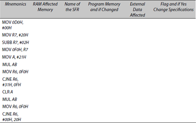
- Fill the codes and mnemonics. Let us assume that a program uses the stack pointer register to save 8 variables in the register bank 3 again after arranging in reverse order these variables at register bank 3 in R0, R1, … , R6 and R7. (For example, R7 becomes R0.) Let the user program area start from 0080H.
8051 initializes the SP = 07H by default at start up. Therefore, the SP is not specifically initialized in the following program. This is because the variables used in the program are in internal RAM from 18H to 1FH (bank3), and n the total number of pushes minus the number of pops does not exceed 8 at any stage of the program. Therefore, SP first increments on each push and reaches maximum up to 0FH only. Hence, the RAM used by the stack top and stack bottom is only between 08H and 0FH. The stack overflow does not affect the array of 8 variables used here in the program.
; Program Exercise
; Program for LIFO operations to reverse the 8 variables arrangement in a register set ; Program application is in rearranging the ascending order data into descending order data ; Program for showing uses of the stack pointer register to save 8 variables in the register ; bank 3
; again after arranging in reverse order these variables at register bank 3 in R0, R1, … , R6 and R7.
; (For example, R7 becomes R0.)
; Raj Kamal July 17, 2009
; Runs on 8051 from the Power up start. User program area starts from 0080H.
; Variable declarations—Register bank 3 R0, R1, R2, R3, R4, R5, R6 and R7
; ISR_VECTADDR area for the ISRs starts from 0x0003 (Refer Table 3.20)
; org 0x0080
