
Chapter 4. Single Supply Op Amp Design Techniques
Ron Mancini
4.1. Single Supply versus Dual Supply
The previous chapter assumed that all op amps were powered from dual or split supplies, and this is not the case in today's world of portable, battery powered equipment. When op amps are powered from dual supplies (see Figure 4.1), the supplies are normally equal in magnitude, opposing in polarity, and the center tap of the supplies is connected to ground. Any input sources connected to ground are automatically referenced to the center of the supply voltage, so the output voltage is automatically referenced to ground.
 |
| Figure 4.1 Split supply op amp circuit. |
Single supply systems do not have the convenient ground reference of dual supply systems, therefore biasing must be employed to ensure that the output voltage swings between the correct voltages. Input sources connected to ground are actually connected to a supply rail in single supply systems. This is analogous to connecting a dual supply input to the minus power rail. This requirement for biasing the op amp inputs to achieve the desired output voltage swing complicates single supply designs.
When the signal source is not referenced to ground (see Figure 4.2), the voltage difference between ground and the reference voltage is amplified along with the signal. Unless the reference voltage was inserted as a bias voltage, and such is not the case when the input signal is connected to ground, the reference voltage must be stripped from the signal so that the op amp can provide maximum dynamic range.
 |
| Figure 4.2 Split supply op amp circuit with reference voltage input. |
An input bias voltage is used to eliminate the reference voltage when it must not appear in the output voltage (see Figure 4.3). The voltage, VREF, is in both input circuits; hence it is named a common mode voltage. Voltage feedback op amps reject common mode voltages because their input circuit is constructed with a differential amplifier (chosen because it has natural common mode voltage rejection capabilities).
 |
| Figure 4.3 Split supply op amp circuit with common mode voltage. |
When signal sources are referenced to ground, single supply op amp circuits exhibit a large input common mode voltage. Figure 4.4 shows a single supply op amp circuit that has its input voltage referenced to ground. The input voltage is not referenced to the midpoint of the supplies, as in a split supply application, rather it is referenced to the lower power supply rail. This circuit does not operate when the input voltage is positive, because the output voltage would have to go to a negative voltage, hard to do with a positive supply. It operates marginally with small negative input voltages, because most op amps do not function well when the inputs are connected to the supply rails.
 |
| Figure 4.4 Single supply op amp circuit. |
The constant requirement to account for inputs connected to ground or different reference voltages makes it difficult to design single supply op amp circuits. Unless otherwise specified, all op amp circuits discussed in this chapter are single supply circuits. The single supply may be wired with the negative or positive lead connected to ground, but as long as the supply polarity is correct, the wiring does not affect circuit operation.
Use of a single supply limits the polarity of the output voltage. When the supply voltage VCC = 10 V, the output voltage is limited to the range 0 ≤ VOUT ≤ 10. This limitation precludes negative output voltages when the circuit has a positive supply voltage, but it does not preclude negative input voltages when the circuit has a positive supply voltage. As long as the voltage on the op amp input leads does not become negative, the circuit can handle negative input voltages.
Beware of working with negative (positive) input voltages when the op amp is powered from a positive (negative) supply because op amp inputs are highly susceptible to reverse voltage breakdown. Also, ensure that all possible startup conditions do not reverse bias the op amp inputs when the input and supply voltage are of opposite polarity.
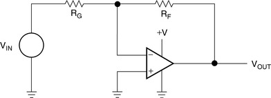
4.2. Circuit Analysis
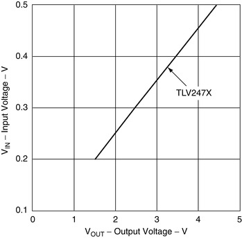
The complexities of single supply op amp design are illustrated with the following example. Note that the biasing requirement complicates the analysis by presenting several nonrealizable conditions. It is best to wade through this material to gain an understanding of the problem, especially since a cookbook solution is given later in this chapter. The previous chapter assumed that the op amps were ideal, and this chapter starts to deal with op amp deficiencies. The input and output voltage swings of many op amps are limited, as shown in Figure 4.7, but if one designs with the selected rail to rail op amps, the input/output swing problems are minimized. The inverting circuit shown in Figure 4.5 is analyzed first.
 |
| Figure 4.5 Inverting op amp. |
Equation (4.1) is written with the aid of superposition and simplified algebraically to acquire Equation (4.2):
(4.1)
(4.2)
As long as the load resistor, RL, has a large value, it does not enter into the circuit calculations, but it can introduce some second order effects, such as limiting the output voltage swings. Equation (4.3) is obtained by setting VREF equal to VIN, and there is no output voltage from the circuit regardless of the input voltage. The author unintentionally designed a few of these circuits before he created an orderly method of op amp circuit design. Actually, a real circuit has a small output voltage equal to the lower transistor saturation voltage, which is about 150 mV for a TLC07X.
(4.3)
When VREF = 0, VOUT = –VIN(RF/RG), there are two possible solutions to Equation (4.2). First, when VIN is any positive voltage, VOUT should be negative voltage. The circuit cannot achieve a negative voltage with a positive supply, so the output saturates at the lower power supply rail. Second, when VIN is any negative voltage, the output spans the normal range according to Equation (4.5):
(4.4)
(4.5)
When VREF equals the supply voltage, VCC, we obtain Equation (4.6). In Equation (4.6), when VIN is negative, VOUT should exceed VCC; that is impossible, so the output saturates. When VIN is positive, the circuit acts as an inverting amplifier.
(4.6)
The transfer curve for the circuit shown in Figure 4.6 (VCC = 5 V, RG = RF = 100 kΩ, RL = 10 kΩ) is shown in Figure 4.7.
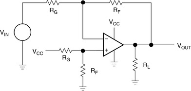 |
| Figure 4.6 Inverting op amp with VCC bias. |
 |
| Figure 4.7 Transfer curve for an inverting op amp with VCC bias. |
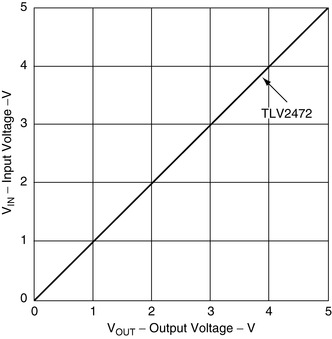
Four op amps were tested in the circuit configuration shown in Figure 4.6. Three of the old generation op amps (LM358, TL07X, and TLC272) had output voltage spans of 2.3 V to 3.75 V. This performance does not justify the ideal op amp assumption made in the previous chapter unless the output voltage swing is severely limited. Limited output or input voltage swing is one of the worst deficiencies a single supply op amp can have, because the limited voltage swing limits the circuit's dynamic range. Also, the limited voltage swing frequently results in distortion of large signals. The fourth op amp tested was the newer TLV247X, which was designed for rail to rail operation in single supply circuits. The TLV247X plotted a perfect curve (results limited by the instrumentation), and it amazed the author with a textbook performance that justifies the use of ideal assumptions. Some of the older op amps must limit their transfer equation as shown in Equation (4.7):
(4.7)
The noninverting op amp circuit is shown in Figure 4.8. Equation (4.8) is written with the aid of superposition and simplified algebraically to acquire Equation (4.9):

(4.8)
(4.9)
 |
| Figure 4.8 Noninverting op amp. |
When VREF = 0,  , two circuit solutions are possible. First, when VIN is a negative voltage, VOUT must be a negative voltage. The circuit cannot achieve a negative output voltage with a positive supply, so the output saturates at the lower power supply rail. Second, when VIN is a positive voltage, the output spans the normal range, as shown by Equation (4.11):

(4.10)
(4.11)
The noninverting op amp circuit is shown in Figure 4.8 with VCC = 5 V, RG = RF = 100 kΩ, and RL = 10 kΩ. The transfer curve for this circuit is shown in Figure 4.9; a TLV247X serves as the op amp.
 |
| Figure 4.9 Transfer curve for a noninverting op amp. |
There are many possible variations of inverting and noninverting circuits. At this point, many designers analyze these variations, hoping to stumble on the one that solves the circuit problem. Rather than analyze each circuit, it is better to learn how to employ simultaneous equations to render specified data into equation form. When the form of the desired equation is known, a circuit that fits the equation is chosen to solve the problem. The resulting equation must be a straight line, therefore only four solutions are possible.
4.3. Simultaneous Equations
Taking an orderly path to developing a circuit that works the first time starts here: Follow these steps until the equation of the op amp is determined. Use the specifications given for the circuit coupled with simultaneous equations to determine what form the op amp equation must have. Go to the section that illustrates that equation form (called a case), solve the equation to determine the resistor values, and you have a working solution.
A linear op amp transfer function is limited to the equation of a straight line:
(4.12)
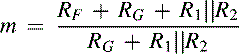
The equation of a straight line has four possible solutions, depending on the sign of m, the slope, and b, the intercept; therefore simultaneous equations yield solutions in four forms. Four circuits must be developed, one for each form of the equation of a straight line. The four equations, cases, or forms of a straight line are given in (4.13)(4.14)(4.15) and (4.16), where electronic terminology has been substituted for math terminology:


(4.13)
(4.14)
(4.15)
(4.16)
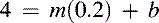
Given a set of two data points for VOUT and VIN, simultaneous equations are solved to determine m and b for the equation that satisfies the given data. The signs of m and b determine the type of circuit required to implement the solution. The given data are derived from the specifications; that is, a sensor output signal ranging from 0.1 V to 0.2 V must be interfaced into an analog to digital converter that has an input voltage range of 1 V to 4 V. These data points (VOUT = 1 V at VIN = 0.1 V, VOUT = 4 V at VIN = 0.2 V) are inserted into Equation (4.13), as shown in (4.17) and (4.18), to obtain m and b for the specifications: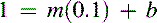
(4.17)
(4.18)
After algebraic manipulation of Equation (4.17), substitute (4.17)(4.18)(4.19) and (4.20) to obtain (Equation 4.21):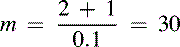
(4.21)
Note: Although Equation (4.13) was the starting point, the form of Equation (4.22) is identical to the format of Equation (4.14). The specifications or given data determine the signs of m and b; and starting with Equation (4.13), the final equation form is discovered after m and b are calculated. The next step required to complete the problem solution is to develop a circuit that has m = 30 and b = −2. Circuits were developed for (4.13)(4.14)(4.15) and (4.16) and they are given under the headings Case 1 through Case 4, respectively. Different circuits yield the same equations, but these circuits were selected because they require no negative references.
4.3.1. Case 1. VOUT = mVIN + b
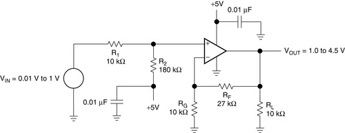
The circuit configuration that yields a solution for Case 1 is shown in Figure 4.10. The figure includes two 0.01 μF capacitors. These capacitors, called decoupling capacitors, are included to reduce noise and provide increased noise immunity. Sometimes two 0.01 μF capacitors serve this purpose, sometimes more extensive filtering is needed, and sometimes one capacitor serves this purpose. Special attention must be paid to the regulation and noise content of VCC when VCC is used as a reference, because some portion of the noise content of VCC is multiplied by the circuit gain.
 |
| Figure 4.10 Schematic for Case 1, VOUT = +mVIN + b. |
The circuit equation is written using the voltage divider rule and superposition: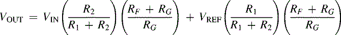
(4.23)
The equation of a straight line (Case 1) is repeated in Equation (4.24) so comparisons can be made between it and Equation (4.23):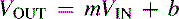
(4.24)


For example, the circuit specifications are VOUT = 1 V at VIN = 0.01 V, VOUT = 4.5 V at VIN = 1 V, RL = 10 k, 5% resistor tolerances, and VCC = 5 V. No reference voltage is available, so VCC is used for the reference input, and VREF = 5 V. A reference voltage source is left out of the design as a space and cost saving measure, and it sacrifices noise performance, accuracy, and stability performance. Cost is an important specification, but the VCC supply must be specified well enough to do the job. Each step in the subsequent design procedure is included in this analysis to ease learning and increase boredom. Many steps are skipped when subsequent cases are analyzed.
The data are substituted into simultaneous equations:

(4.27)
(4.28)
Equation (4.27) is multiplied by 100, (4.29) and (4.28) is subtracted from Equation (4.29) to obtain Equation (4.30):
(4.29)
(4.30)
The slope of the transfer function, m, is obtained by substituting b into Equation (4.27):
(4.31)
Now that b and m are calculated, the resistor values can be calculated. (4.25) and (4.26) are solved for the quantity (RF + RG)/RG, then they are set equal in Equation (4.32), yielding Equation (4.33):

(4.32)
(4.33)
Resistors of 5% tolerance are specified for this design, so we choose R1 = 10 kΩ, and that sets the value of R2 = 183.16 kΩ. The closest 5% resistor value to 183.16 kΩ is 180 kΩ; therefore select R1 = 10 kΩ and R2 = 180 kΩ. Being forced to yield to reality by choosing standard resistor values means that there is an error in the circuit transfer function, because m and b are not exactly the same as calculated. The real world constantly forces compromises into circuit design, but the good circuit designer accepts the challenge and throws money or brains at the challenge. Resistor values closer to the calculated values could be selected by using 1% or 0.5% resistors, but that selection increases cost and violates the design specification. The cost increase is hard to justify except in precision circuits. Using 10 cent resistors with a 10 cent op amp usually is false economy.

The resulting circuit equation is
(4.36)
The gain setting resistor, RG, is selected as 10 kΩ, and 27 kΩ, the closest 5% standard value is selected for the feedback resistor, RF. Again, a slight error is involved with standard resistor values. This circuit must have an output voltage swing from 1 V to 4.5 V. The older op amps cannot be used in this circuit, because they lack dynamic range, so the TLV247X family of op amps is selected. The data shown in Figure 4.7 confirm the op amp selection because there is little error. The circuit with the selected component values is shown in Figure 4.11. The circuit was built with the specified components, and the transfer curve is shown in Figure 4.12.
 |
| Figure 4.11 Case 1 example circuit. |
 |
| Figure 4.12 Case 1 example circuit measured transfer curve. |
The transfer curve shown is a straight line, which means that the circuit is linear. The VOUT intercept is about 0.98 V rather than 1 V as specified, and this is excellent performance, considering that the components were selected randomly from bins of resistors. Different sets of components would have slightly different slopes because of the resistor tolerances. The TLV247X has input bias currents and input offset voltages, but the effect of these errors is hard to measure on the scale of the output voltage. The output voltage measured 4.53 V when the input voltage was 1 V. Considering the low and high input voltage errors, it is safe to conclude that the resistor tolerances have skewed the gain slightly, but this is still excellent performance for 5% components. Often lab data similar to that shown here is more accurate than the 5% resistor tolerance, but do not fall into the trap of expecting this performance, because you will be disappointed if you do.
The resistors were selected in the kilo-ohm range arbitrarily. The gain and offset specifications determine the resistor ratios, but supply current, frequency response, and op amp drive capability determine their absolute values. The resistor value selection in this design is high because modern op amps do not have input current offset problems and they yield reasonable frequency response. If higher frequency response is demanded, the resistor values must decrease, and resistor value decreases reduce input current errors, while supply current increases. When the resistor values get low enough, it becomes hard for another circuit, or possibly the op amp, to drive the resistors.
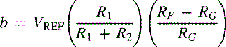
4.3.2. Case 2. VOUT = +mVIN − b
The circuit shown in Figure 4.13 yields a solution for Case 2. The circuit equation is obtained by taking the Thevenin equivalent circuit looking into the junction of R1 and R2. After the R1, R2 circuit is replaced with the Thevenin equivalent circuit, the gain is calculated with the ideal gain equation, Equation (4.37):
(4.37)
 |
| Figure 4.13 Schematic for Case 2, VOUT = +mVIN − b. |
The specifications for an example design are VOUT = 1.5 V at VIN = 0.2 V, VOUT = 4.5 V at VIN = 0.5 V, VREF = VCC = 5 V, RL = 10 kΩ, and 5% resistor tolerances. The simultaneous equations follow:

(4.40)
(4.41)
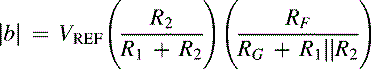
From these equations, we find that b = −0.5 and m = 10. Making the assumption that R1‖R2 ≪ RG simplifies the calculations of the resistor values:

(4.42)
(4.43)
Let RG = 20 kΩ and RF = 180 kΩ:

(4.44)
(4.45)
Select R2 = 0.82 kΩ and R1 = 72.98 kΩ. Since 72.98 kΩ is not a standard 5% resistor value, R1 is selected as 75 kΩ. The difference between the selected and calculated value of R1 has about a 3% effect on b, and this error shows up in the transfer function as an intercept rather than a slope error. The parallel resistance of R1 and R2 is approximately 0.82 kΩ, and this is much less than RG, which is 20 kΩ, thus the earlier assumption that RG ≫ R1‖R2 is justified. R2 could have been selected as a smaller value, but the smaller values yielded poor standard 5% values for R1. The final circuit is shown in Figure 4.14 and the measured transfer curve for this circuit is shown in Figure 4.15.
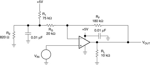 |
| Figure 4.14 Case 2 example circuit. |
 |
| Figure 4.15 Case 2 example circuit measured transfer curve. |
The TLV247X was used to build the test circuit because of its wide dynamic range. The transfer curve plots very close to the theoretical curve; the direct result of using a high performance op amp.
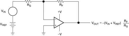
4.3.3. Case 3. VOUT = −mVIN + b
The circuit shown in Figure 4.16 yields the transfer function desired for Case 3.
 |
| Figure 4.16 Schematic for Case 3, VOUT = −mVIN + b. |
The circuit equation is obtained with superposition: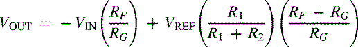
(4.46)

The design specifications for an example circuit are VOUT = 1 V at VIN = −0.1 V, VOUT = 6 V at VIN = −1 V, VREF = VCC = 10 V, RL = 100 Ω, and 5% resistor tolerances. The supply voltage available for this circuit is 10 V, and this exceeds the maximum allowable supply voltage for the TLV247X. Also, this circuit must drive a back terminated cable that looks like two 50 Ω resistors connected in series, so the op amp must be able to drive 6/100 = 60 mA. The stringent op amp selection criteria limits the choice to relatively new op amps if ideal op amp equations are going to be used. The TLC07X has excellent single supply input performance coupled with high output current drive capability, so it is selected for this circuit. The simultaneous equations, (4.49) and (4.50), follow: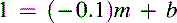

(4.49)
(4.50)
From these equations, we find that b = 0.444 and m = −5.6: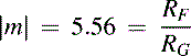
(4.51)
(4.52)
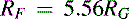
Let RG = 10 kΩ and RF = 56.6 kΩ, which is not a standard 5% value, hence RF is selected as 56 kΩ:

(4.53)
(4.54)
The final equation for the example follows:
(4.55)
Select R1 = 2 kΩ and R2 = 295.28 kΩ. Since 295.28 kΩ is not a standard 5% resistor value, R1 is selected as 300 kΩ. The difference between the selected and calculated values of R1 has a nearly insignificant effect on b. The final circuit is shown in Figure 4.17 and the measured transfer curve for this circuit is shown in Figure 4.18.
 |
| Figure 4.17 Case 3 example circuit. |
 |
| Figure 4.18 Case 3 example circuit measured transfer curve. |
As long as the circuit works normally, there are no problems handling the negative voltage input to the circuit, because the inverting lead of the TLC07X is at a positive voltage. The positive op amp input lead is at a voltage of approximately 65 mV, and normal op amp operation keeps the inverting op amp input lead at the same voltage because of the assumption that the error voltage is zero. When VCC is powered down while there is a negative voltage on the input circuit, most of the negative voltage appears on the inverting op amp input lead.
The most prudent solution is to connect the diode, D1, with its cathode on the inverting op amp input lead and its anode at ground. If a negative voltage gets on the inverting op amp input lead, it is clamped to ground by the diode. Select the diode type as germanium or Schottky so the voltage drop across the diode is about 200 mV; this small voltage does not harm most op amp inputs. As a further precaution, RG can be split into two resistors with the diode inserted at the junction of the two resistors. This places a current limiting resistor between the diode and the inverting op amp input lead.
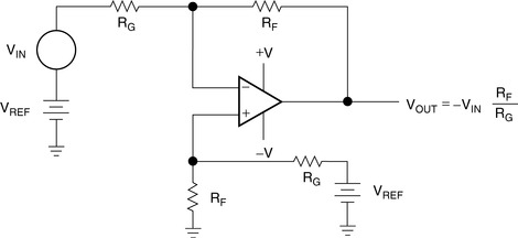
4.3.4. Case 4. VOUT = −mVIN − b
The circuit shown in Figure 4.19 yields a solution for Case 4. The circuit equation is obtained by using superposition to calculate the response to each input. The individual responses to VIN and VREF are added to obtain Equation (4.56):
(4.56)
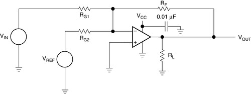 |
| Figure 4.19 Schematic for Case 4, VOUT = −mVIN − b. |


The design specifications for an example circuit are VOUT = 1 V at VIN = −0.1 V, VOUT = 5 V at VIN = −0.3 V, VREF = VCC = 5 V, RL = 10 kΩ, and 5% resistor tolerances. The simultaneous (4.59) and (4.60) follow:
(4.59)
(4.60)
From these equations, we find that b = −1 and m = −20. Setting the magnitude of m equal to Equation (4.57) yields Equation (4.61):

(4.61)
(4.62)
Let RG1 = 1 kΩ and RF = 20 kΩ:

(4.63)
(4.64)
The final equation for this example is
(4.65)
The final circuit is shown in Figure 4.20 and the measured transfer curve for this circuit is shown in Figure 4.21.
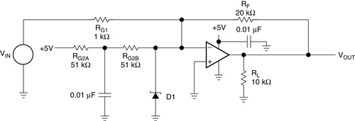 |
| Figure 4.20 Case 4 example circuit. |
 |
| Figure 4.21 Case 4 example circuit measured transfer curve. |
The TLV247X was used to build the test circuit because of its wide dynamic range. The transfer curve plots very close to the theoretical curve, and this results from using a high performance op amp.
As long as the circuit works normally, there are no problems handling the negative voltage input to the circuit because the inverting lead of the TLV247X is at a positive voltage. The positive op amp input lead is grounded, and normal op amp operation keeps the inverting op amp input lead at ground because of the assumption that the error voltage is zero when VCC is powered down while there is a negative voltage on the inverting op amp input lead.
The most prudent solution is to connect the diode D1 with its cathode on the inverting op amp input lead and its anode at ground. If a negative voltage gets on the inverting op amp input lead, it is clamped to ground by the diode. Select the diode type as germanium or Schottky, so the voltage drop across the diode is about 200 mV; this small voltage does not harm most op amp inputs. RG2 is split into two resistors (RG2A = RG2B = 51 kΩ) with a capacitor inserted at the junction of the two resistors. This places a power supply filter in series with VCC.
4.4. Summary
Single supply op amp design is more complicated than split supply op amp design, but with a logical design approach, excellent results are achieved. Single supply design used to be considered technically limiting, because older op amps had limited capability. The new op amps, such as the TLC247X, TLC07X, and TLC08X, have excellent single supply parameters; therefore when used in the correct applications, these op amps yield rail to rail performance equal to their split supply counterparts.
Single supply op amp design usually involves some form of biasing, and this requires more thought, so single supply op amp design needs discipline and a procedure. The recommended procedure for single supply op amp design is
• Substitute the specification data into simultaneous equations to obtain m and b (the slope and intercept of a straight line).
• Let m and b determine the form of the circuit.
• Choose the circuit configuration that fits the form.
• Using the circuit equations for the circuit configuration selected, calculate the resistor values.
• Build the circuit, take data, and verify performance.
• Test the circuit for nonstandard operating conditions (circuit power off while interface power is on, over- or underrange inputs, etc.).
• Add protection components as required.
• Retest.
When this procedure is followed, good results follow. As single supply circuit designers expand their horizon, new challenges require new solutions. Remember, the only equation a linear op amp can produce is the equation of a straight line. That equation has only four forms. The new challenges may consist of multiple inputs, common mode voltage rejection, or something different, but this method can be expanded to meet these challenges.
..................Content has been hidden....................
You can't read the all page of ebook, please click here login for view all page.