
Chapter 9. Current Feedback Op Amp Analysis
Ron Mancini
9.1. Introduction
Current feedback amplifiers (CFA) do not have the traditional differential amplifier input structure, therefore they sacrifice the parameter matching inherent to that structure. The CFA circuit configuration prevents them from obtaining the precision of voltage feedback amplifiers (VFA), but the circuit configuration that sacrifices precision results in increased bandwidth and slew rate. The higher bandwidth is relatively independent of closed loop gain, so the constant gain/bandwidth restriction applied to VFAs is removed for CFAs. The slew rate of CFAs is much improved from their counterpart VFAs, because their structure enables the output stage to supply slewing current until the output reaches its final value. In general, VFAs are used for precision and general purpose applications, while CFAs are restricted to high frequency applications, above 100 MHz.
Although CFAs lack the precision of their VFA counterparts, they are precise enough to be DC coupled in video applications, where dynamic range requirements are not severe. CFAs, unlike previous generation high frequency amplifiers, have eliminated the AC coupling requirement; they are usually DC coupled while they operate in the gigahertz range. CFAs have much faster slew rates than VFAs, so they have faster rise and fall times and less intermodulation distortion.
9.2. CFA Model
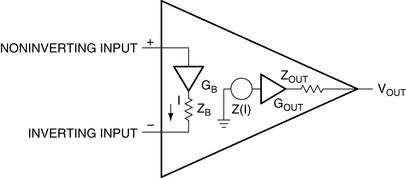
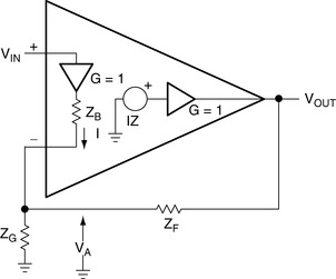
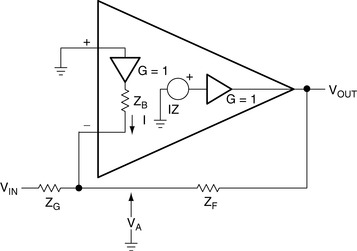
The CFA model is shown in Figure 9.1. The noninverting input of a CFA connects to the input of the input buffer, so it has very high impedance, similar to that of a bipolar transistor noninverting VFA input. The inverting input connects to the input buffer's output, so the inverting input impedance is equivalent to a buffer's output impedance, which is very low. ZB models the input buffer's output impedance, and it is usually less than 50 Ω. The input buffer gain, GB, is as close to 1 as IC design methods can achieve, and it is small enough to neglect in the calculations.
 |
| Figure 9.1 Current feedback amplifier model. |
The output buffer provides low output impedance for the amplifier. Again, the output buffer gain, GOUT, is very close to 1, so it is neglected in the analysis. The output impedance of the output buffer is ignored during the calculations. This parameter may influence the circuit performance when driving very low impedance or capacitive loads, but this is usually not the case. The input buffer's output impedance can't be ignored because it affects stability at high frequencies.
The current controlled current source, Z, is a transimpedance. The transimpedance in a CFA serves the same function as gain in a VFA: It is the parameter that makes the performance of the op amp dependent only on the passive parameter values. Usually the transimpedance is very high, in the megaohm range, so the CFA gains accuracy by closing a feedback loop in the same manner as the VFA.
9.3. Development of the Stability Equation
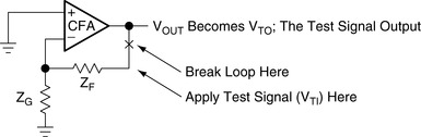
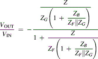
The stability equation is developed with the aid of Figure 9.2 Remember, stability is independent of the input and depends solely on the loop gain, Aβ. Breaking the loop at point X, inserting a test signal, VTI, and calculating the return signal, VTO, develops the stability equation.
 |
| Figure 9.2 Stability analysis circuit. |
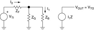
The circuit used for stability calculations is shown in Figure 9.3, where the model of Figure 9.1 is substituted for the CFA symbol. The input and output buffer gain and the output buffer output impedance have been deleted from the circuit to simplify calculations. This approximation is valid for almost all applications.
 |
| Figure 9.3 Stability analysis circuit. |
The transfer equation is given in Equation (9.1) and Kirchhoff's law is used to write (9.2) and (9.3):

(9.1)
(9.2)
(9.3)
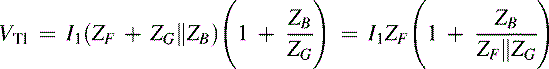
Dividing Equation (9.1) by Equation (9.4) yields Equation (9.5) and this is the open loop transfer equation. This equation is commonly known as the loop gain.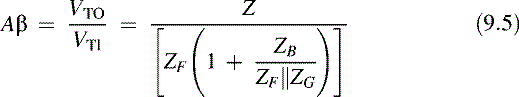
(9.5)
9.4. The Noninverting CFA
The closed loop gain equation for the noninverting CFA is developed with the aid of Figure 9.4, where external gain setting resistors have been added to the circuit. The buffers are shown in Figure 9.4, but because their gains equal 1 and they are included within the feedback loop, the buffer gain does not enter into the calculations.
 |
| Figure 9.4 Noninverting CFA. |
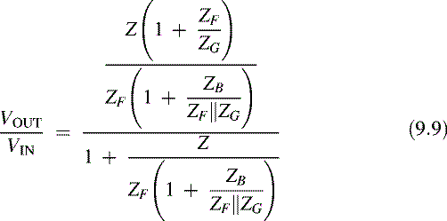
Equation (9.6) is the transfer equation, Equation (9.7) is the current equation at the inverting node, and Equation (9.8) is the input loop equation. These equations are combined to yield the closed loop gain equation, Equation (9.9).

(9.6)
(9.7)
(9.8)
(9.9)
When the input buffer output impedance, ZB, approaches zero, Equation (9.9) reduces to Equation (9.10):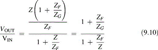
(9.10)
When the transimpedance, Z, is very high, the term ZF/Z in Equation (9.10) approaches zero, and Equation (9.10) reduces to Equation (9.11), the ideal closed loop gain equation for the CFA. The ideal closed loop gain equations for the CFA and VFA are identical, and the degree to which they depart from ideal depends on the validity of the assumptions. The VFA has one assumption, that the direct gain is very high, while the CFA has two assumptions, that the transimpedance is very high and the input buffer output impedance is very low. As would be expected, two assumptions are much harder to meet than one, so the CFA departs from the ideal more than the VFA.
(9.11)
9.5. The Inverting CFA
The inverting CFA configuration (Figure 9.5) is seldom used, because the inverting input impedance is very low (ZB‖ZF + ZG). When ZG is made dominant by selecting it as a high resistance value, it overrides the effect of ZB. ZF must also be selected as a high value to achieve at least unity gain, and high values for ZF result in poor bandwidth performance, as we see in the next section. If ZG is selected as a low value, the frequency sensitive ZB causes the gain to increase as frequency increases. These limitations restrict inverting applications of the inverting CFA.
 |
| Figure 9.5 Inverting CFA. |
The current equation for the input node is written as Equation (9.12). Equation (9.13) defines the dummy variable VA, and Equation (9.14) is the transfer equation for the CFA. These equations are combined and simplified, leading to Equation (9.15), which is the closed loop gain equation for the inverting CFA.

(9.12)
(9.13)
(9.14)
(9.15)

When Z is very large, Equation (9.16) becomes Equation (9.17), which is the ideal closed loop gain equation for the inverting CFA:
(9.17)
The ideal closed loop gain equation for the inverting VFA and CFA op amps are identical. Both configurations have lower input impedance than the noninverting configuration, but the VFA has one assumption while the CFA has two assumptions. Again, as was the case with the noninverting counterparts, the CFA is less ideal than the VFA because of the two assumptions. The zero ZB assumption always breaks down in bipolar junction transistors, as is shown later. The CFA is almost never used in the differential amplifier configuration because of the CFA's gross input impedance mismatch.
9.6. Stability Analysis
The stability equation is repeated as (Equation 9.18):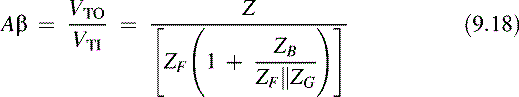
(9.18)
Comparing (9.9)(9.15)(9.16)(9.17) and (9.18) reveals that the inverting and noninverting CFA op amps have identical stability equations. This is the expected result because stability of any feedback circuit is a function of the loop gain, and the input signals have no effect on stability. The two op amp parameters affecting stability are the transimpedance, Z, and the input buffer's output impedance, ZB. The external components affecting stability are ZG and ZF. The designer controls the external impedance, although stray capacitance that is a part of the external impedance sometimes seems to be uncontrollable. Stray capacitance is the primary cause of ringing and overshooting in CFAs. Z and ZB are CFA op amp parameters that can't be controlled by the circuit designer, who has to live with them.
Prior to determining stability with a Bode plot, we take the log of Equation (9.18) and plot the logs, (9.19) and (9.20), in Figure 9.6: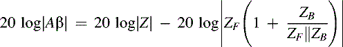
(9.19)
(9.20)
 |
| Figure 9.6 Bode plot of stability equation. |
This enables the designer to add and subtract components of the stability equation graphically.
The transimpedance has two poles, and the plot shows that the op amp is unstable without the addition of external components, because 20 log|Z| crosses the 0 dB axis after the phase shift is 180°. ZF, ZB, and ZG reduce the loop gain 61.1 dB, so the circuit is stable because it has a 60° phase margin. ZF is the component that stabilizes the circuit. The parallel combination of ZF and ZG contribute little to the phase margin, because ZB is very small, so ZB and ZG have little effect on stability.
The manufacturer determines the optimum value of RF during the characterization of the IC. Referring to Figure 9.6, we see that, when RF exceeds the optimum value recommended by the IC manufacturer, stability increases. The increased stability has a price, called decreased bandwidth. Conversely, when RF is less than the optimum value recommended by the IC manufacturer, stability decreases, and the circuit response to step inputs is overshooting or possibly ringing. Sometimes the overshoot associated with less than optimum RF is tolerated because the bandwidth increases as RF decreases. The peaked response associated with less than optimum values of RF can be used to compensate for cable droop caused by cable capacitance.
When ZB = 0 Ω and ZF = RF, the loop gain equation is Aβ = Z/RF. Under these conditions, Z and RF determine stability, and a value of RF can always be found to stabilize the circuit. The transimpedance and feedback resistor have a major impact on stability, and the input buffer's output impedance has a minor effect on stability. Since ZB increases with an increase in frequency, it tends to increase stability at higher frequencies. Equation (9.18) is rewritten as Equation (9.24), but it has been manipulated so that the ideal closed loop gain is readily apparent:
(9.24)
The closed loop ideal gain equation (inverting and noninverting) shows up in the denominator of Equation (9.24), so the closed loop gain influences the stability of the op amp. When ZB approaches zero, the closed loop gain term also approaches zero, and the op amp becomes independent of the ideal closed loop gain. Under these conditions RF determines stability, and the bandwidth is independent of the closed loop gain. Many people claim that the CFA bandwidth is independent of the gain, and that claim's validity depends on the ratio ZB/ZF being very low.
ZB is important enough to warrant further investigation, so the equation for ZB follows: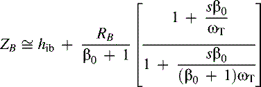
(9.25)
At low frequencies hib = 50 Ω and RB/(β0 + 1) = 25, so ZB = 75 Ω. ZB varies in accordance with Equation (9.25) at high frequencies. Also, the transistor parameters in Equation (9.25) vary with transistor type; they are different for NPN and PNP transistors. Because ZB depends on the output transistors used, and this is a function of the quadrant the output signal is in, ZB has an extremely wide variation. ZB is a small factor in the equation, but it adds a lot of variability to the current feedback op amp.
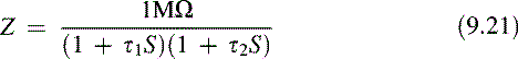
9.7. Selection of the Feedback Resistor
The feedback resistor determines stability, and it affects closed loop bandwidth, so it must be selected very carefully. Most CFA IC manufacturers employ applications and product engineers who spend a great deal of time and effort selecting RF. They measure each noninverting gain with several feedback resistors to gather data. Then they pick a compromise value of RF that yields stable operation with acceptable peaking, and that value of RF is recommended on the data sheet for that specific gain. This procedure is repeated for several gains in anticipation of the various gains customer applications require (often G = 1, 2, or 5). When the value of RF or the gain is changed from the values recommended on the data sheet, bandwidth and/or stability is affected.
A circuit designer who must select a different RF value from that recommended on the data sheet gets into stability or low bandwidth problems. Lowering RF decreases stability, and increasing RF decreases bandwidth. What happens when the designer needs to operate at a gain not specified on the data sheet? The designer must select a new value of RF for the new gain, but there is no guarantee that new value of RF is an optimum value. One solution to the RF selection problem is to assume that the loop gain, Aβ, is a linear function. Then, the assumption can be made that (Aβ)1 for a gain of 1 equals (Aβ)N for a gain of N, and that this is a linear relationship between stability and gain. (9.26) and (9.27) are based on the linearity assumption: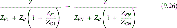
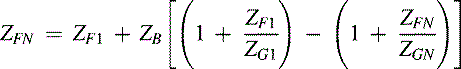
(9.26)
(9.27)
Equation (9.27) leads one to believe that a new value ZF can easily be chosen for each new gain. This is not the case in the real world; the assumptions don't hold up well enough to rely on them. When changing to a new gain not specified on the data sheet, Equation (9.27), at best, supplies a starting point for RF, but it must be tested to determine the final value of RF.
When the RF value recommended on the data sheet can't be used, an alternate method of selecting a starting value for RF is to use graphical techniques. The graph shown in Figure 9.7 is a plot of the typical 300 MHz CFA data given in Table 9.1.
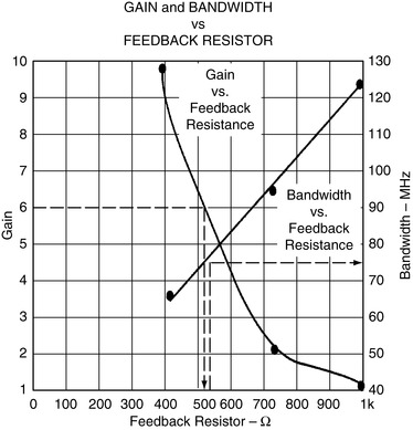 |
| Figure 9.7 Plot of CFA RF, gain, and bandwidth. |
| Gain (ACL) | RF (Ω) | Bandwidth (MHz) |
|---|---|---|
| +1 | 1000 | 125 |
| +2 | 681 | 95 |
| +10 | 383 | 65 |
Enter the graph at the new gain, say ACL = 6, and move horizontally until you reach the intersection of the gain versus feedback resistance curve. Then, drop vertically to the resistance axis and read the new value of RF (500 Ω in this example). Enter the graph at the new value of RF and travel vertically until you intersect the bandwidth versus feedback resistance curve. Now, move to the bandwidth axis to read the new bandwidth (75 MHz in this example). As a starting point, you should expect to get approximately 75 MHz bandwidth with a gain of 6 and RF = 500 Ω. Although this technique yields more reliable solutions than Equation (9.27), op amp peculiarities, circuit board stray capacitances, and wiring make extensive testing mandatory. The circuit must be tested for performance and stability at each new operating point.
9.8. Stability and Input Capacitance
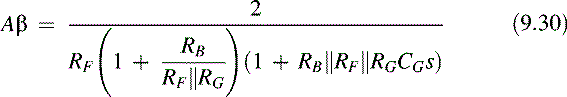
When the designer lets the circuit board introduce stray capacitance on the inverting input node to ground, it causes the impedance ZG to become reactive. The new impedance, ZG, is given in (9.28) and (9.29) is the stability equation that describes the situation: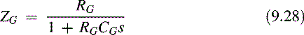

(9.28)
(9.29)
(9.30)
Equation (9.29) is the stability equation when ZG consists of a resistor in parallel with stray capacitance between the inverting input node and ground. The stray capacitance, CG, is a fixed value because it depends on the circuit layout. The pole created by the stray capacitance depends on RB because it dominates RF and RG. RB fluctuates with manufacturing tolerances, so the RBCG pole placement is subject to IC manufacturing tolerances. As the RBCG combination becomes larger, the pole moves toward the zero frequency axis, lowering the circuit stability. Eventually it interacts with the pole contained in Z, 1/T2, and instability results.
The effects of stray capacitance on CFA closed loop performance are shown in Figure 9.8.
 |
| Figure 9.8 Effects of stray capacitance on CFAs. |
Note that the introduction of CG causes more than 3 dB peaking in the CFA frequency response plot, and it increases the bandwidth about 18 MHz. Two picofarads are not a lot of capacitance, because a sloppy layout can easily add 4 pF or more to the circuit.
9.9. Stability and Feedback Capacitance
When a stray capacitor is formed across the feedback resistor, the feedback impedance is given by Equation (9.31). Equation (9.32) gives the loop gain when a feedback capacitor has been added to the circuit.

(9.31)
(9.32)
This loop gain transfer function contains a pole and zero, therefore, depending on the pole/zero placement, oscillation can result. The Bode plot for this case is shown in Figure 9.9. The original and composite curves cross the 0 dB axis with a slope of –40 dB/decade, so either curve can indicate instability. The composite curve crosses the 0 dB axis at a higher frequency than the original curve, hence the stray capacitance has added more phase shift to the system. The composite curve is surely less stable than the original curve. Adding capacitance to the inverting input node or across the feedback resistor usually results in instability. RB largely influences the location of the pole introduced by CF, so here is another case where stray capacitance leads to instability.
 |
| Figure 9.9 Bode plot with CF. |
Figure 9.8 shows that CF = 2 pF adds about 4 dB of peaking to the frequency response plot. The bandwidth increases about 10 MHz because of the peaking. CF and CG are the major causes of overshooting, ringing, and oscillation in CFAs; and the circuit board layout must be carefully done to eliminate these stray capacitances.
9.10. Compensation of CF and CG
When both CF and CG are present in the circuit, they may be adjusted to cancel out each other. The stability equation for a circuit with CF and CG is Equation (9.33):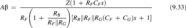
(9.33)
If the zero and pole in Equation (9.33) are made to cancel each other, the only poles remaining are in Z. Setting the pole and zero in Equation (9.33) equal yields Equation (9.34) after some algebraic manipulation: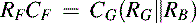
(9.34)
RB dominates the parallel combination of RB and RG, so Equation (9.34) is reduced to Equation (9.35):
(9.35)
RB is an IC parameter, so it depends on the IC process. RB it is an important IC parameter, but it is not important enough to be monitored as a control variable during the manufacturing process. RB has widely spread, unspecified parameters; so depending on RB for compensation is risky. Rather, the prudent design engineer assures that the circuit will be stable for any reasonable value of RB and the resulting frequency response peaking is acceptable.
9.11. Summary
Constant gain/bandwidth is not a limiting criterion for the CFA, so the feedback resistor is adjusted for maximum performance. Stability depends on the feedback resistor: As RF is decreased, stability is decreased; and when RF goes to zero, the circuit becomes unstable. As RF is increased stability increases, but the bandwidth decreases.
The inverting input impedance is very high, but the noninverting input impedance is very low. This situation precludes CFAs from operation in the differential amplifier configuration. Stray capacitance on the inverting input node or across the feedback resistor always leads to peaking, usually to ringing, and sometimes to oscillations. A prudent circuit designer scans the PC board layout for stray capacitances and eliminates them. Breadboarding and lab testing are a must with CFAs. The CFA performance can be improved immeasurably with a good layout, good decoupling capacitors, and low inductance components.
..................Content has been hidden....................
You can't read the all page of ebook, please click here login for view all page.