
Chapter 2. Review of Circuit Theory
Ron Mancini
2.1. Introduction
Although this book minimizes math, some algebra is germane to the understanding of analog electronics. Math and physics are presented here in the manner in which they are used later, so no practice exercises are given. For example, after the voltage divider rule is explained, it is used several times in the development of other concepts, and this usage constitutes practice.
Circuits are a mix of passive and active components. The components are arranged in a manner that enables them to perform some desired function. The resulting arrangement of components is called a circuit or sometimes a circuit configuration. The art portion of analog design is developing the circuit configuration. Many published circuit configurations are available for almost any circuit task; therefore, circuit designers need not be artists.
When the design has progressed to the point that a circuit exists, equations must be written to predict and analyze circuit performance. Textbooks are filled with rigorous methods for equation writing, and this review of circuit theory does not supplant those textbooks. But, a few equations are used so often that they should be memorized, and these equations are considered here.
A circuit can be analyzed in almost as many ways as there are electronic engineers, and if the equations are written correctly, all methods yield the same answer. There are some simple ways to analyze the circuit without completing unnecessary calculations, and these methods are illustrated here.
2.2. Laws of Physics
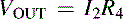
Ohm's law is stated as V = IR, and it is fundamental to all electronics. Ohm's law can be applied to a single component, to any group of components, or to a complete circuit. When the current flowing through any portion of a circuit is known, the voltage dropped across that portion of the circuit is obtained by multiplying the current times the resistance (Equation 2.1):
(2.1)
In Figure 2.1, Ohm's law is applied to the total circuit. The current (I) flows through the total resistance (R), and the voltage (V) is dropped across R.
 |
| Figure 2.1 Ohm's law applied to the total circuit. |
In Figure 2.2, Ohm's law is applied to a single component. The current (IR) flows through the resistor (R) and the voltage (VR) is dropped across R. Note: The same formula is used to calculate the voltage drop across R even though it is only a part of the circuit.
 |
| Figure 2.2 Ohm's law applied to a component. |
Kirchhoff's voltage law states that the sum of the voltage drops in a series circuit equals the sum of the voltage sources. Otherwise, the source (or sources) voltage must be dropped across the passive components. When taking sums keep in mind that the sum is an algebraic quantity. Kirchhoff's voltage law is illustrated in Figure 2.3 and (2.2) and (2.3):

(2.2)
(2.3)
 |
| Figure 2.3 Kirchhoff's voltage law. |
Kirchhoff's current law states that the sum of the currents entering a junction equals the sum of the currents leaving a junction. It makes no difference if a current flows from a current source, through a component, or through a wire, because all currents are treated identically. Kirchhoff's current law is illustrated in Figure 2.4 and (2.4) and (2.5):
(2.4)
(2.5)
 |
| Figure 2.4 Kirchhoff's current law. |
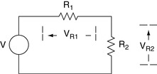
2.3. Voltage Divider Rule
When the output of a circuit is not loaded, the voltage divider rule can be used to calculate the circuit's output voltage. Assume that the same current flows through all circuit elements (Figure 2.5). Equation (2.6) is written using Ohm's law as V = I (R1 + R2). Equation (2.7) is written as Ohm's law across the output resistor.

(2.6)
(2.7)
 |
| Figure 2.5 Voltage divider rule. |

A simple way to remember the voltage divider rule is that the output resistor is divided by the total circuit resistance. This fraction is multiplied by the input voltage to obtain the output voltage. Remember that the voltage divider rule always assumes that the output resistor is not loaded; the equation is not valid when the output resistor is loaded by a parallel component. Fortunately, most circuits following a voltage divider are input circuits, and input circuits are usually high resistance circuits. When a fixed load is in parallel with the output resistor, the equivalent parallel value comprising the output resistor and loading resistor can be used in the voltage divider calculations with no error. Many people ignore the load resistor if it is 10 times greater than the output resistor value, but this will lead to a 10% error.
2.4. Current Divider Rule
When the output of a circuit is not loaded, the current divider rule can be used to calculate the current flow in the output branch circuit (R2). The currents I1 and I2 in Figure 2.6 are assumed to be flowing in the branch circuits. Equation (2.9) is written with the aid of Kirchhoff's current law. The circuit voltage is written in Equation (2.10) with the aid of Ohm's law. Combining (2.9) and (2.10) yields Equation (2.11).


(2.9)
(2.10)
(2.11)
 |
| Figure 2.6 Current divider rule. |

The total circuit current divides into two parts, and the resistance (R1) divided by the total resistance determines how much current flows through R2. An easy method of remembering the current divider rule is to remember the voltage divider rule. Then, modify the voltage divider rule such that the opposite resistor is divided by the total resistance and the fraction is multiplied by the input current to get the branch current.
2.5. Thevenin's Theorem
At times, it is advantageous to isolate a part of the circuit to simplify the analysis of the isolated part of the circuit rather than write loop or node equations for the complete circuit and solve them simultaneously. Thevenin's theorem enables us to isolate the part of the circuit we are interested in. We then replace the remaining circuit with a simple series equivalent circuit, thus Thevenin's theorem simplifies the analysis.
Two theorems do similar functions. The Thevenin theorem, just described, is the first, and the second is called Norton's theorem. Thevenin's theorem is used when the input source is a voltage source, and Norton's theorem is used when the input source is a current source. Norton's theorem is rarely used, so its explanation is left for the reader to dig out of a textbook if it is ever required.
The rules for Thevenin's theorem start with the component or part of the circuit being replaced. Referring to Figure 2.7 look back into the terminals (left from C and R3 toward point X–X in the figure) of the circuit being replaced. Calculate the no load voltage (VTH) as seen from these terminals (use the voltage divider rule).
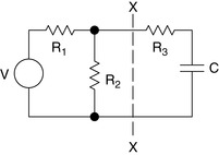 |
| Figure 2.7 Original circuit. |
Look into the terminals of the circuit being replaced, short independent voltage sources, and calculate the impedance between these terminals. The final step is to substitute the Thevenin equivalent circuit for the part you wanted to replace, as shown in Figure 2.8.
 |
| Figure 2.8 Thevenin's equivalent circuit for Figure 2.7. |
The Thevenin equivalent circuit is a simple series circuit, thus further calculations are simplified. The simplification of circuit calculations is often sufficient reason to use Thevenin's theorem, because it eliminates the need for solving several simultaneous equations. The detailed information about what happens in the circuit that was replaced is not available when using Thevenin's theorem, but that is no consequence because you had no interest in it.
As an example of Thevenin's theorem, let's calculate the output voltage (VOUT) shown in Figure 2.9(a). The first step is to stand on the terminals X–Y with your back to the output circuit and calculate the open circuit voltage seen (VTH). This is a perfect opportunity to use the voltage divider rule to obtain Equation (2.13):
(2.13)
 |
| Figure 2.9 Example of Thevenin's equivalent circuit. |
Still standing on the terminals X–Y, step 2 is to calculate the impedance seen looking into these terminals (short the voltage sources). The Thevenin impedance is the parallel impedance of R1 and R2, as calculated in Equation (2.14). Now, get off the terminals X–Y before you damage them with your big feet. Step 3 replaces the circuit to the left of X–Y with the Thevenin equivalent circuit VTH and RTH.
(2.14)
(Note: Two parallel vertical bars (‖) are used to indicate parallel components.)
The final step is to calculate the output voltage. Note that the voltage divider rule is used again. Equation (2.15) describes the output voltage, and it comes out naturally in the form of a series of voltage dividers, which makes sense. That's another advantage of the voltage divider rule: The answers normally come out in a recognizable form rather than a jumble of coefficients and parameters.
(2.15)
The circuit analysis is done the hard way in Figure 2.10, so you can see the advantage of using Thevenin's theorem. Two loop currents, I1 and I2, are assigned to the circuit. Then, the loop (2.16) and (2.17) are written:

(2.16)
(2.17)
 |
| Figure 2.10 Analysis done the hard way. |
Equation (2.17) is rewritten as Equation (2.18) and substituted into Equation (2.16) to obtain Equation (2.19):

(2.18)
(2.19)
The terms are rearranged in Equation (2.20). Ohm's law is used to write Equation (2.21) and the final substitutions are made in Equation (2.22).

(2.20)
(2.21)
(2.22)
This is a lot of extra work for no gain. Also, the answer is not in a usable form because the voltage dividers are not recognizable. Therefore, more algebra is required to get the answer into usable form.
2.6. Superposition
Superposition is a theorem that can be applied to any linear circuit. Essentially, when there are independent sources, the voltages and currents resulting from each source can be calculated separately, and the results are added algebraically. This simplifies the calculations, because it eliminates the need to write a series of loop or node equations. An example is shown in Figure 2.11.
 |
| Figure 2.11 Superposition example. |
When V1 is grounded, V2 forms a voltage divider with R3 and the parallel combination of R2 and R1. The output voltage for this circuit (VOUT2) is calculated with the aid of the voltage divider Equation (2.23). The circuit is shown in Figure 2.12. The voltage divider rule yields the answer quickly.
(2.23)
 |
| Figure 2.12 When V1 is grounded. |
Likewise, when V2 is grounded (Figure 2.13), V1 forms a voltage divider with R1 and the parallel combination of R3 and R2, and the voltage divider theorem is applied again to calculate VOUT, Equation (2.24):
(2.24)
 |
| Figure 2.13 When V2 is grounded. |
After the calculations for each source are made, the components are added to obtain the final solution, Equation (2.25):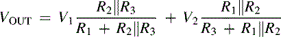
(2.25)
The reader should analyze this circuit with loop or node equations to gain an appreciation for superposition. Again, the superposition results come out as a simple arrangement that is easy to understand. One looks at the final equation and it is obvious that, if the sources are equal and opposite polarity and R1 = R3, then the output voltage is zero. Conclusions such as this are hard to make after the results of a loop or node analysis unless considerable effort is made to manipulate the final equation into symmetrical form.
2.7. Calculation of a Saturated Transistor Circuit
The circuit specifications are these: When VIN = 12 V, VOUT < 0.4 V at ISINK < 10 mA, and VIN < 0.05 V, VOUT > 10 V at IOUT = 1 mA. The circuit diagram is as shown in Figure 2.14.
 |
| Figure 2.14 Saturated transistor circuit. |
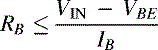
The collector resistor must be sized, Equation (2.26), when the transistor is off, because it has to be small enough to allow the output current to flow through it without dropping more than 2 V to meet the specification for a 10 V output:
(2.26)
When the transistor is off, 1 mA can be drawn out of the collector resistor without pulling the collector or output voltage to less than 10 V, Equation (2.27). When the transistor is on, the base resistor must be sized, Equation (2.28), to enable the input signal to drive enough base current into the transistor to saturate it. The transistor beta is 50.
(2.27)
(2.28)

When the transistor goes on, it sinks the load current, and it still goes into saturation. These calculations neglect some minor details, but they are in the 98% accuracy range.
2.8. Transistor Amplifier
The amplifier is an analog circuit (Figure 2.15), and the calculations, plus the points that must be considered during the design, are more complicated than for a saturated circuit. This extra complication leads people to say that analog design is harder than digital design (the saturated transistor is digital, i.e., on or off). Analog design is harder than digital design because the designer must account for all states in analog, whereas only two states must be accounted for in digital. The specifications for the amplifier are an AC voltage gain of 4 and a peak to peak signal swing of 4 V.
 |
| Figure 2.15 Transistor amplifier. |
IC is selected as 10 mA because the transistor has a current gain (β) of 100 at that point. The collector voltage is arbitrarily set at 8 V; when the collector voltage swings positive 2 V (from 8 V to 10 V), enough voltage still is dropped across RC to keep the transistor on. Set the collector/emitter voltage at 4 V; when the collector voltage swings negative 2 V (from 8 V to 6 V), the transistor still has 2 V across it, so it stays linear. This sets the emitter voltage (VE) at 4 V.

(2.30)
(2.31)
Use Thevenin's equivalent circuit to calculate R1 and R2, as shown in Figure 2.16:

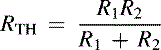
(2.32)
(2.33)
(2.34)
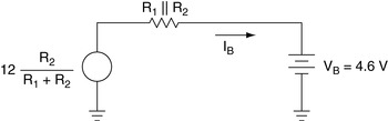 |
| Figure 2.16 Thevenin equivalent of the base circuit. |
We want the base voltage to be 4.6 V because the emitter voltage is then 4 V. Assume a voltage drop of 0.4 V across RTH, so Equation (2.35) can be written. The drop across RTH may not be exactly 0.4 V because of beta variations, but a few hundred millivolts does not matter in this design. Now, calculate the ratio of R1 and R2 using the voltage divider rule (the load current has been accounted for).


(2.35)
(2.36)
(2.37)
R1 is almost equal to R2, thus selecting R1 as twice the Thevenin resistance yields approximately 4 k, as shown in Equation (2.35). Hence, R1 = 11.2 k and R2 = 8 k. The AC gain is approximately RC/RE1 because CE shorts out RE2 at high frequencies, so we can write Equation (2.38):

(2.38)
(2.39)
The capacitor selection depends on the frequency response required for the amplifier, but 10 μF for CIN and 1000 μF for CE suffice for a starting point.
..................Content has been hidden....................
You can't read the all page of ebook, please click here login for view all page.