
Chapter 6. Characteristics of Formal Equivalency Verification
6.1 RTL Combinational Model Equivalency
A critical SoC project checkpoint at multiple phases of the development schedule is to prove functional equivalency between the RTL and gate netlist implementation model throughout the SoC model hierarchy. An RTL logic synthesis flow is expected to remain equivalent through the various stages of logic reduction, factoring, repowering, technology library mapping, and clock/ test insertion algorithms. Yet for gate netlists that are manually captured or, especially, for ECOs applied directly to the netlist, model equivalency between RTL and netlist must be proven. Functional validation testbenches applied to both RTL and netlist is a possible approach to evaluating equivalency, although such an approach is not exhaustive. EDA vendors offer a toolset to formally prove (combinational) logical equivalency between two models: RTL-to-RTL, RTL-to-gate, or gate-to-gate netlists).
The equivalency methodology utilizes the concept of a logic cone, as illustrated in Figure 6.1.

Figure 6.1 An endpoint signal for a logic equivalency test (or a path timing test) is driven by a set of inputs that define a logic cone.
The endpoint of a logic cone, or equivalency testpoint, is a state element output or primary output of the model. The logic cone inputs are the comprehensive set of fan-in signals to the testpoint, traversed back through combinational logic to state element outputs and model primary inputs. The equivalency flow begins by constructing the logic cones in each of the two models through identifying the testpoints in the model and tracing backward to construct the logic network, stopping at the cone inputs. Once a correspondence is established between all test points in the two models (as described in the next section), algorithms are applied to compare the logic cone functionality.
Note that combinational logic equivalency is based on the register-transfer level (RTL) paradigm. State elements are explicitly defined in the HDL model description (and no combinational feedback loops are present). This enables the direct identification of testpoints and a logic cone traversal algorithm that results in a directed acyclic graph (DAG) with precise levelization.
6.2 State Mapping for Equivalency
As mentioned in the previous section, once the sets of logic cones are constructed for the two models, the next step in the equivalency flow is assigning correspondence between each testpoint in one model to a testpoint in the other. This state mapping step is heuristic in nature, employing a number of algorithms to investigate the two models (e.g., common testpoint signal names, cones that share the same input signal list). Note that state mapping is iterative: Confirming that two cones have the same inputs for testpoint correspondence requires prior correspondence of the fan-in signal list. To expedite state mapping, it is recommended to maintain RTL-to-gate testpoint signal name correlation wherever possible and use common primary input/output port names between the two models. EDA tools also accept a user input file, in which designers can provide recommendations for state correspondence to guide the mapping algorithms.
The user input file to the equivalency flow also identifies instances in the RTL and netlist hierarchies that are black boxes, not part of the logic cones. As illustrated in Figure 6.2, the pins of a black box introduce additional cones for analysis. This method would be applied to exclude arrays and any mixed-signal IP. It would also be used in support of a hierarchical equivalency methodology, in which child nodes in the two parent models have already been proven equivalent.
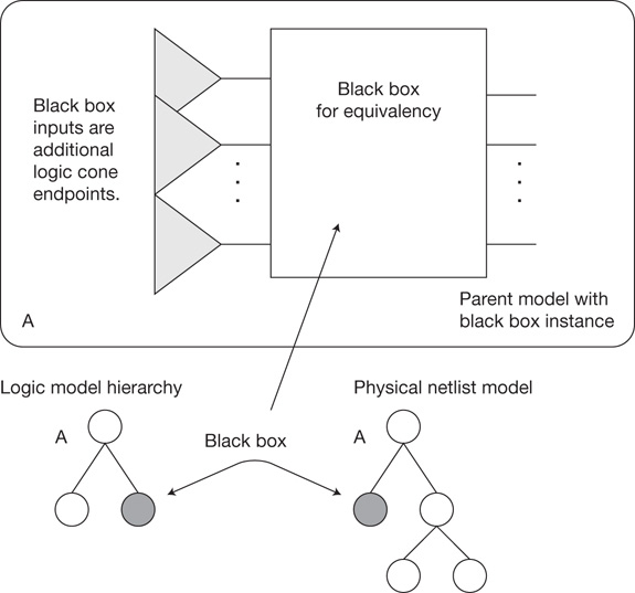
Figure 6.2 A black box is defined in both models for instances that have been previously verified for equivalency. The input pins of the black box are added to the set of endpoint tests. The output pins of the black box serve as additional logic cone inputs.
The normal situation is that a 1:1 state mapping correspondence is established between the two models. A special case arises if the implementation model has made a parallel copy of the testpoint, as depicted in Figure 6.3. The EDA tool would need to support a 1:n state mapping and equivalency proof.
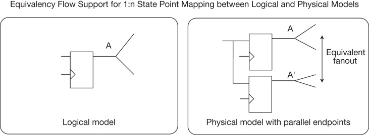
Figure 6.3 Parallel copies of an endpoint (in the physical model) require a 1:n mapping description to be provided to the equivalency flow.
Note also that there will be connections in the gate netlist that are not present in the RTL model; for example, the result of scan test logic insertion will alter the logic cone inputs with signals such as “scan_enable”. In addition to a user input description with state mapping guidance to the equivalency flow, a set of logic signals and their Boolean values to apply during equivalency will be needed to disable logic not pertinent to the equivalency comparison. (Section 5.7 discusses the focus on scan validation at the netlist level and the difficulties in representing the physical scan implementation back to the RTL model.)
One additional difference that may arise during state mapping is a logic inversion between the RTL and gate models, as illustrated in Figure 6.4.
The EDA tool may support recognition of the two cones in Figure 6.4 as inverse equivalent and propagate the logic inversion property for the cones where the testpoint is in the fan-in list.

Figure 6.4 An inverse equivalent endpoint in the two models could be accepted by the EDA tool, which will propagate the inversion property as the input to other logic cones.
6.3 Combinational Logic Cone Analysis
In general, the equivalence-proving algorithms make no prior assumptions on any similarities between internal logic cone signals in the two models. Also, the execution runtime increases with the input size of the cone. As a result, the formal proof may be subject to a “time limit exceeded” for a very large cone, a setting provided to the EDA tool by the equivalency flow. The EDA tool may also include a number of heuristic algorithms to look for potential additional (combinational) correspondence points within the two cones to reduce the effective size. Equivalence checking of different versions of RTL-to-RTL or gate-to-gate netlist models leverages this internal correspondence and is thus relatively straightforward. RTL-to-gate equivalency is more difficult to prove for large cones, although the adoption of RTL logic signal names within the gate netlist when feasible is certainly beneficial.
6.3.1 Equivalency Debug
The results of the equivalency flow fall into several categories:
Incomplete logic cone endpoint mapping (If the initial testpoint correspondence step in the flow is not completed, additional user input to provide mapping recommendations will be required.)
Cone too large, timeout during comparison (Again, additional input guidance to suggest [internal] cone signal correspondence between the two models will be needed.)
Cones equivalent
Cones provably different
If there is a provable difference between the cones of the two models, the EDA tool provides additional information to assist with further investigation. At a minimum, one or more vectors applied at the inputs to the cones are generated, highlighting the different calculated testpoint values. Additional tool debug features may present visual representations of the logic in the two cones, with the evaluated results from an applied vector annotated to signals within each cone. A key diagnostic feature would be to identify logic present in the “overlapping cones” of failing testpoints, as depicted in Figure 6.5.

Figure 6.5 A debug aid for an equivalency error is to identify overlapping logic in failing cones, reducing the network size within which to search for a logical difference.
Assuming that one model is “golden,” the overlapping logic in failing cones in the other model is a likely source of the logic discrepancy. In general, the diagnosis of the root cause of RTL-to-gate equivalency mismatches is difficult, especially for large cones.
6.4 Use of Model Input Assertions for Equivalency
The previous sections in this chapter highlight some of the user input information that can help accelerate the equivalency flow. Another special case relates to the additional use of logic assertions. Figure 6.6 illustrates a simple example in which an assertion between netlist input signals is required to establish correspondence and evaluate equivalence.

Figure 6.6 To support equivalency verification of models with different pinouts, assertions may be provided to the flow. The figure illustrates that the netlist model for a block uses both polarities of a primary input port. These assertions need to be independently proven.
For completeness, any model assertions used in the equivalency flow need to be (formally) proven separately, such as with an EDA property prover tool.
6.5 Sequential Model Equivalency
Section 4.1 described the use of behavioral logic synthesis when the SoC model incorporates sequential process statements with inferred signal states. A key factor in the adoption of sequential synthesis is the corresponding availability of sequential logic equivalency checking tools from EDA vendors. These tools utilize methods that are related to model prover algorithms, as they must represent the behavior of a model over some number of clock cycles.
The general problem of sequential equivalence is illustrated in Figure 6.7.

Figure 6.7 General methodology for demonstrating sequential equivalence for two general logic networks. (Note that a common initial state between the two models is assumed.)
Some facets to sequential logic equivalence are significantly more complex than combinational equivalence. Figure 6.8 illustrates how logic is moved across state testpoints as part of sequential path timing optimization.

Figure 6.8 As part of sequential timing optimization, logic may be moved across state points. Sequential equivalency verification is significantly more complex than a combinational logic cone proof.
Another example of a complex sequential optimization addresses power reduction using sequential clock gating, as illustrated in Figure 6.9.
The finite state machine implementations in the behavioral HDL and sequential synthesis output models may differ significantly, as with the sequential power gating topology in Figure 6.9. An algorithmic approach to sequential equivalency would begin in an initial state for the combined network of the two models, as depicted in Figure 6.7. Analysis would proceed by computing the set of reachable states over multiple clock cycles. The set of reachable states grows in cycle n+1, based on the current state in cycle n plus a specific vector of inputs. The sequential equivalence algorithm ends when the reachable state set is unchanged in successive cycles.[1,2,3]If the calculated model_1 and model_2 outputs do not differ throughout the reachability analysis, sequential equivalency is demonstrated.

Figure 6.9 Example of sequential clock gating.
The general complexity of sequential equivalence is reduced when the application is to verify a behavioral model to the corresponding RTL model generated by behavioral synthesis. The task of transitively checking the equivalence of a gate netlist logic ECO to updated RTL (using combinational equivalence) and ultimately back to an updated behavioral model is more involved.
6.6 Functional and Test-Mode Equivalence Verification
Section 6.4 briefly discusses the user inputs to the functional equivalence flow, including Boolean assignments to exclude netlist logic and signal connectivity that is not part of the HDL model. The typical application of these input assertions is to exclude test logic, which would commonly be inserted during the logic synthesis flow. Another area to exclude would be any netlist-level functionality associated with power gating control that is inserted during synthesis using the power format input file description. A unique area where significant logic is likely to be added to the netlist that may not be present in the HDL is the on-chip e-fuse array controller. (The fuses are programmed during production test to insert redundant SRAM resources for manufacturing defects detected on the die, after executing memory BIST pattern sequences.) In all cases of input assertions applied to modify the netlist (or HDL) model for equivalence, the methodology team needs to identify the validation strategy to evaluate the functionality of the excluded logic. Assuming that the constraints are primarily associated with the netlist model, a suite of gate-level simulation testcases is required.
The platform for simulating the netlist model, combined with the expected testcase workload, requires estimating the EDA tool licenses and compute resources to be allocated. Fortunately, the frequency of running gate-level simulation tests is typically low. The expectation is that test and power gating logic insertion algorithms will be error free, and MBIST repair-focused testcases need only be run infrequently. For any simulations used to augment functional equivalency verification, special attention needs to be given to the coverage criteria. As the netlist model is used, the EDA tools that analyze RTL-based line/expression/path coverage would not apply; manually developed coverage analysis is needed.
6.7 Array Equivalence Verification
Section 5.5 introduces symbolic simulation technology, which is typically used in conjunction with reduction of a transistor-level netlist to a logic model, and the reduction of (bus) signals to symbol representations. Symbols are propagated through the model during testcase execution. The complexity of simulation results increases with each successive clock cycle, which limits the general applicability of this technology. One area to which symbolic simulation is well-suited is the evaluation of memory array behavior in both an RTL model and a reduced transistor netlist.
A special class of equivalence verification compares the behavior of an RTL IP model to the device netlist used for physical implementation. For simple IP cells, such as the elements of a standard cell library, demonstrating model equivalence is relatively straightforward, using one of the following methods:
Exhaustive testcase simulation of the RTL logic and transistor switch simulation models
Reduction of channel-connected regions (CCRs) to an equivalent logic model for input to equivalency verification
(Simple) symbolic simulation testcases
Figure 6.10 illustrates these equivalency options for a logic cell.

Figure 6.10 Illustration of switch-level simulation, channel-connected region (CCR) identification and model generation, and symbolic simulation for a logic cell.
The demonstration of the equivalency of the RTL and netlist models for an SRAM array IP offering strictly uses symbolic simulation. A set of testcases is written for each array operation and applied to the RTL and device netlist models. As the number of clock cycles required to complete an array operation is typically few, the complexity of the symbolic simulation results (and the model output comparisons) is manageable.
EDA vendors offer specific products for array equivalence verification, embedding a symbolic simulator into a framework for testcase development, simulation results visualization, and discrepancy debugging (see Figure 6.11).

Figure 6.11 Illustration of symbolic simulation requirements for an SRAM array. Unique topology identification algorithms are required to manage the (large) CCR topologies for dotted bitcells. Timed signals generated internally to the array result in complex simulation symbols.
To help ensure the success of this approach, the EDA vendor makes recommendations on the functionality to include/exclude from the array. The hierarchical boundary for array equivalence should exclude random logic, if at all possible, which would quickly add to the internal simulation symbol complexity. The array internal model may include registered input/output data values; although the clock cycle depth in testcases will be longer in this case, the complexity of the simulated results does not increase substantially, as the symbolic data value is not altered. Array circuits often include transistor size ratios that enable “strong” active devices to overwrite “weak” devices (e.g., weak bit line pullup devices versus the active devices driving bit lines in the array bitcell). The EDA vendor also enables the designer to define how device size ratios should be modeled as part of the initial transistor array netlist reduction.
6.8 Summary
The SoC methodology team must present a comprehensive strategy for demonstrating the equivalence of the (tapeout) netlist to the HDL model used for functional validation. Manually designed IP requires equivalency to be demonstrated between the implementation schematic and the corresponding HDL model released as part of the IP library. By definition, the output of synthesis flows should be logically equivalent to the HDL. A critical collaboration between the equivalency and functional validation teams is required to examine additional test and power gating logic inserted during synthesis that is not present in the HDL source. Most importantly, the insertion of late (functional or non-functional) ECOs directly to the netlist to expedite implementation, enabling minimal disruption to the existing physical design, must be reflected in the HDL model and quickly verified for equivalence.
The SoC project management team needs to decide when equivalency is required to be demonstrated during the validation and physical design schedule. It is a prerequisite for hard IP promotion to higher levels of physical integration, as well as a tapeout checklist gating item. Additional equivalency milestones may be appropriate, especially during the physical ECO implementation phase. Section 3.1 describes the development of the logical and physical model hierarchies. Correspondence points between these hierarchical models are valid candidates to submit to the equivalency flow. Full-chip equivalence can be demonstrated by equivalence of hierarchy correspondence points, which can then be black boxes when analyzing equivalence at parent nodes.
Finally, the SoC team may also seek to develop specific expertise for debugging equivalency discrepancies. Finding the root cause of logic cone differences between netlist and RTL is not easy. The skills required include detailed knowledge of RTL coding semantics, IP libraries, and synthesis flow algorithms. (Debugging symbolic simulation discrepancies between two models is an additional skill.) The documentation policies used by the SoC project to describe changes in successive revision releases of RTL model versions and (especially) the application of ECOs certainly help pinpoint where differences could have arisen. Nevertheless, the SoC design team may want to develop expertise in the equivalency flow and allocate design engineering resource to assist the validation team during the phases of the project schedule focused on model equivalence verification.
References
[1] Kuehlmann, A., and van Eijk, C., “Combinational and Sequential Equivalence Checking,– Chapter 13 of Logic Synthesis and Verification, S. Hassoun and T. Sasao, Editors, Kluwer Academic, 2001.
[2] Ravi., K. and Somenzi, F., “High-Density Reachability Analysis,– Proceedings of the IEEE International Conference on Computer-Aided Design (ICCAD), 1995, p. 154–158.
[3] van Eijk, C., “Sequential Equivalence Checking Based on Structural Similarities, “IEEE Transactions on Computer Aided Design of Integrated Circuits and Systems, Volume 19, Issue 7, July 2000, pp. 814–819.
Further Research
Array Equivalence
Hard IP memory arrays may include internal data/address registers. Describe techniques for verifying the equivalence of the scan chains through these registers between the HDL and schematic models for the array.
Equivalence Verification with Array Repair
Section 19.3 describes how redundant rows and/or columns incorporated into a memory array may be multiplexed into the array to replace defective bitcells after die production testing. Commonly, on-die fuses are (permanently) programmed after testing to alter the array configuration. This chapter briefly describes (good) array HDL-to-schematic equivalence verification using symbolic simulation. However, methodologies for verifying the full model of redundant array topologies with fuse array programmability are currently rather ad hoc.
Research and propose methods for improving the verification robustness of the full memory array and fuse array model (with shifting of fuse values to array multiplexers).
Data Structures for Equivalence Verification
EDA research has pursued techniques for efficient representation of combinational logic networks for equivalence verification. Many EDA tools use data structures based on the concept of a binary decision diagram (BDD).
Describe the BDD data structure and the advantages/disadvantages of this logic representation for equivalence verification.