
Chapter 14. Power Rail Voltage Drop Analysis
14.1 Introduction to Power Rail Voltage Drop Analysis
The power analysis flow described in Chapter 13, “Power Analysis,” provides power dissipation data used for thermal modeling of the die/package combination and for confirmation of the overall SoC power specification. The power analysis flow also provides localized power dissipation data for hot spot identification. A related analysis flow utilizes switching activity and cell characterization power supply current waveforms to calculate the voltage drop on the VDD power and ground (P/G) distribution rails.
Power rail voltage drop analysis involves applying cell current data to an extracted model for the P/G distribution network (PDN). A resistive P/G mesh model is used for a static I*R voltage drop estimate, while a more elaborate RC extracted model for the PDN is required for a dynamic voltage drop calculation. The RC network for the P/G grids would be merged with the RLCM model for the connections from die pads (through bumps or bond wires) to package pins. The self- and mutual inductances of the top metal redistribution wires from pads to the SoC internal P/G grids may be significant and would also be part of the composite die/package RLCM model.
14.1.1 Conservative Versus Aggressive P/G Grid Design
IP library cells and macros are characterized using an assumed limit on the supply and ground voltage drop from the package pins to the cell/macro location. The power rail analysis flow is used to confirm that these assumptions have not been exceeded.
The design of the cell layout image for the IP library includes the track allocation for the power and ground rails for the block-level and global grids. If the image design is conservative, the impedance of the P/G distribution should be low enough to satisfy the voltage drop limits when any SoC design incorporating this IP is submitted to the power rail analysis flow, regardless of cell placement or switching activity. In other words, the P/G image needs to be sufficiently robust so that the rail analysis should never result in a voltage drop margin error.
A more aggressive SoC project may opt to free up some of the allocated P/G rails to make more tracks available for signal routes if the voltage drop limits can be met with a reduced grid. During SoC global and block floorplanning, a physical integration engineer may opt to populate the P/G grids more sparsely than called for in the original image design. The lower-level metal rails connecting directly to cells and macros would be unaltered, but the intermediate and upper-level grids could be reduced from the IP design recommendation if the switching activity allowed.
As with the power analysis flow in Chapter 13, the SoC methodology needs to support block-level power rail voltage drop analysis for early insight into any P/G issues, especially if any modifications to the recommended image grid design (or decoupling capacitance insertion guidelines) have been pursued.
14.1.2 ASIC Direct Release
The origins of the semi-custom application-specific IC (ASIC) design methodology began with the availability of IP logic library cells placed and routed on a die with a pervasive cell image throughout and with fixed local and global P/G grids. Both standard-cell and gate-array cell library layouts were developed to align with this image. (Standard-cell and gate-array cell design styles are introduced in Section 1.1.) I/O receiver and driver cells also had a fixed placement image, connected to separate VDDIO and GNDIO rails. With this image, ASIC part numbers were offered in a range of logic gate capacities, with corresponding recommendations on cell utilization and decoupling capacitance densities.
The primary image design consideration was that all ASIC designs were expected to have satisfied the P/G voltage drop margins assumed during library cell characterization, regardless of the local cell logic type and drive-strength selections or switching activity factors. The goal was to facilitate the direct release of a placed and routed database to fabrication, without any modifications required to the P/G distribution.
Conservative design assumptions were made when designing the ASIC power and ground rails. For example, as illustrated in Figure 14.1, a high concentration of high-drive-strength cells were placed in a single row; the maximum current in the rail would be the sum of the (saturated) device current in each cell. This local model would be replicated throughout the ASIC die when analyzing the fixed P/G grids. (The figure illustrates cells placed back-to-back in adjacent rows, sharing VDD and GND rails.)

Figure 14.1 Example of a “conservative” ASIC P/G image design assumption, suitable for direct release. It is similar to Figure 10.25 but with cell rows populated with high-drive-strength cells.
With this image released to all customers, the subsequent ASIC designs were essentially assured to be free of power rail voltage drop margin fails. ASIC direct release was facilitated at the expense of metal resources conservatively allocated to the P/G grids.
With the emergence of SoC designs integrating a wide diversity of IP macros and cores, the direct-release, fixed-image design style is no longer feasible. As a result, there is an opportunity to pursue a more aggressive P/G design approach. Individual blocks may develop a unique internal P/G distribution. The trade-off for the aggressive PDN design is that the power rail voltage drop analysis flow is required to be exercised throughout the physical implementation project phase on both block and full-chip SoC physical integration releases.
14.1.3 P/G for Blocks with sleepFETs
A special methodology is required for power rail analysis of a sleepFET configuration, as depicted in Figure 13.4. The extracted network for GNDinternal and GNDglobal is separated by the sleepFET cells. The P/G network model needs to be augmented prior to power rail analysis of the active block, with effective Ron values inserted for each sleepFET device. (The turn-off and turn-on P/G currents when transitioning to/from a sleep state are outside the scope of the power rail analysis flow, as a time-dependent simulation is required to reflect the delays of the enable signal to the distributed sleepFET cells.)
14.2 Static I*R Rail Analysis
Static I*R voltage drop analysis uses DC currents injected into the resistive model. This calculation is much quicker than the dynamic rail analysis with a full RLCM model. Also, I*R static analysis can be pursued with a partial SoC physical design; the DC currents for blocks with an initial physical implementation can be merged with (coarse) estimates for the current of other blocks/channels and applied to the resistive network of the P/G grid.
Any excessive rail voltage drop from static I*R analysis is indicative of a design issue that needs to be addressed, without the addition of dynamic voltage analysis results. To fix static I*R flow failures, the P/G grid may need additional density, wider rails, and/or improved via arrays between metal layers.
The static I*R analysis flow is specifically applied to any distinct power domains created for analog mixed-signal IP. The DC current profile for the mixed-signal block would be derived from the IP power model or from detailed circuit simulation measures, if available. Ideally, the current profile model includes precise physical location granularity to be annotated to the nodes of the extracted analog P/G mesh.
14.2.1 Static I*R Matrix Solution
The algorithmic solution for the static I*R flow is represented as the nodal analysis formulation of the matrix equation:
using Kirchhoff’s current law (KCL) at each node. In the equation above, G is the (very sparse) conductance matrix between nodes of the extracted VDD (or GND) distribution network, i is the vector of DC currents injected at these nodes, and v is the node voltage vector to solve. As illustrated in Figure 14.2, the elements of the (symmetric) conductance matrix consist of diagonal entries equal to the sum of all conductances connected to node i (conductance G = 1/R), and the off-diagonal values are the negative of the conductance between nodes i and j in the extracted resistive power grid network.
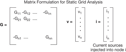
Figure 14.2 Illustration of the conductance matrix G used in the static I*R solution.
A number of approaches have been developed to solve this type of very large, very sparse matrix problem.[1]
14.3 Dynamic P/G Voltage Drop Analysis
A more accurate analysis of the P/G distribution is provided by the dynamic voltage drop flow, based on the supply current data from the cell characterization tables and the switching activity of (stressmark) patterns applied to the netlist model, as described in Section 13.2. The time-dependent current sources generate P/G rail voltage drops that combine the resistive losses and inductive impedance from the package and chip redistribution layer wires, offset by the (local) capacitance.
14.3.1 P/G Rail Capacitance
The capacitances in the dynamic RC power rail model include several contributions, as illustrated in Figure 14.3:
Distributed capacitance of the power and ground rails
Explicit decoupling capacitance cells added to the design
Device node capacitance connected to the rail
Device well capacitance to substrate

Figure 14.3 Sources of explicit and internal capacitances on the PDN (similar to Figure 10.26).
The device capacitances that may assist in providing a low-impedance path for voltage noise depend on the operating mode of the device—whether active or off. The well-to-substrate junction capacitance includes a significant series resistance due to the high sheet resistivity of both these nodes and is thus less effective in filtering rail noise.
The parasitic extraction flow directed to the P/G net names provides only the RC parasitics of the rails. The other capacitance contributors reside inside cells and need to be specifically added to the nodes of the extracted RC network as part of the rail analysis flow. Explicit decoupling capacitance cells are readily located and added to the grid electrical model. An “averaging” algorithm is needed for active and off device node capacitance elements added to the model.
Note that P/G parasitic extraction requires special features. In general, RC reduction is not applied, to enable decoupling capacitance cells to be accurately assigned to their corresponding location; this non-reduced network is also used for power rail electromigration analysis (see Chapter 15, “Electromigration[EM] Reliability Analysis”). An exception would be applied to the reduction of metal via arrays to an equivalent resistance and capacitance to reduce the extracted model dataset size, as illustrated in Figure 14.4.

Figure 14.4 Illustration of the reduction of via arrays in the P/G grids to an equivalent resistance and capacitance.
The package P/G pin RLCM electrical models are connected to the extracted RC (or RLCM) model of the global P/G grid, and the additional device and decoupling capacitances are included. Recall that the definition of the inductive impedance requires establishing the area of the current loop of which the wire segment is a constituent. The electrical definition of partial inductance allows a loop to be broken into individual segments for calculation. Once the loop current path is defined, the combination of the individual segment self-inductance and inter-segment mutual inductances allows a full electrical model to be developed.[2] The SoC design team should closely evaluate the loop model assumptions used in preparing the individual inductive elements in the RLCM network used for dynamic P/G voltage drop analysis. Note that the package (and die RDL) current loop model should include mutual inductances between VDD and GND package pins and metal traces, necessitating a combined dynamic analysis of both grids.
14.3.2 Matrix Solution
Circuit simulation of the dynamic P/G model presents extreme challenges due to the size of the extracted RC network, augmented with the addition of the decoupling and parasitic capacitances, the time-dependent current sources, and the package model. Note that the dynamic power grid analysis model is relatively constrained, consisting solely of RLCM elements, local current sources, and supply voltage sources applied at package pins; no non-linear device models are present. Rather than attempt traditional simulation, a matrix formulation and incremental timestep solution is typically pursued. The previous section briefly describes the conductance matrix used to represent the network for static I*R voltage drop analysis. Similarly, dynamic analysis can be represented by an “admittance matrix”:[3]
where G is the conductance matrix, Y is the time derivative matrix, and s is the vector of applied current sources. Whereas the solution vector in the static I*R analysis is the set of network node voltages, the vector x(t) is expanded in the admittance model to include both (time-varying) node voltages plus inductor branch currents. The dynamic analysis proceeds by solving the matrix equation at successive timesteps. Unlike traditional circuit simulation, with adaptive timestep advance algorithms, a fixed timestep interval is used for dynamic P/G analysis. A backward Euler approximation for the time derivative of the solution vector, x'(t), is used in Reference 14.3. Rather than expressing the solution at time increment (n+1) in terms of the value and the derivative at time increment n, the backward Euler method relates the solution at time tn in terms of the value and derivative at tn+1:
where h is the timestep increment, and the first term of the Taylor expansion for x is used. Figure 14.5 illustrates the backward Euler relation (for a one-dimensional curve).

Figure 14.5 Illustration of the backward Euler approach for dynamic P/G analysis timestep solutions. A simple one-dimensional curve (and a close-up of that curve between tn and tn+1) is shown.
To simplify the notation, let:
Equation 14.4 is an approximation of Equation 14.3, neglecting the O(h2) error term. Transforming the general admittance matrix equation into the backward Euler time increment format of Equation 14.4 results in:
The solution vector x(t) is solved at each successive timestep tn+1, using this matrix equation and the solution at time tn. The time-varying current sources in the power grid, s(t), are recalculated at each time increment.
The matrix analysis introduced in the previous section using KCL to solve for node voltages needs to be modified to represent the current through the inductive elements, with:
An example of the matrix formulation is given Figure 14.6 for a simple RLCM network, from Reference 14.4.

Figure 14.6 Example of inductive elements in the admittance matrix for dynamic P/G rail analysis. The G and Y matrix entries reflect the network R, L, C, and M element values connected to nodes b through e.
The inductor branch currents in the solution vector x are represented by the additional rows and columns in the conductance matrix G, with 0, 1, and −1 entries, and by the addition of a sub-matrix to the time-derivative matrix Y, with the self- and mutual inductance values.
A unique optimization to the dynamic matrix model leverages the common topology in which a series resistor is present with the inductor. The time derivative of the inductor current can be equally represented as the time derivative of the resistor voltage, allowing the inductor branch current to be optimized out of the solution vector, as depicted in Figure 14.7.

Figure 14.7 Matrix optimization for a series R and L connection.
To review, the matrices G and Y are populated with the extracted P/G grid and package model network values. The cell source current waveform data are pulled from the characterization tables, using the output load and slew measures determined from static timing analysis. The time-varying source current vector, s, represents these cell currents assigned to P/G network nodes, at the switching times recorded during the power stressmark simulations. (The power supply reference voltage inputs at package pins are also part of the current source vector.) The P/G network voltages at each time step are solved using Equation 14.5. The results of the dynamic simulation would be compared to the P/G rail margin assumptions used for library IP characterization.
14.3.3 Hierarchical Analysis with Abstracted Partition and Global Models
The dynamic power rail network model described above is still very large and is therefore unsuitable for many matrix solver algorithms. Reference 14.3 describes a method for dividing the full-chip P/G analysis into a single global and multiple partition-level models to solve. For global analysis, the partitions are abstracted with their ports attached to nodes in the global grid, as illustrated in Figure 14.8.

Figure 14.8 Illustration of global and partition-level models for dynamic I*R analysis.
The partitioning step typically utilizes the physical floorplan block hierarchy. Each partition-level P/G model is composed solely of RC elements with the annotated local cell current sources. Inductive elements are likely to be present only in the global model.
Consider the global grid model, with abstracts for the partitions. In the figure, the current into each partition model port from the global grid is denoted as ji. The vector j is of length M, where M is the number of partition ports. The goal of the dynamic rail analysis at the global level is two-fold:
Measure the time-varying node voltages for the global RLCM model, using the extracted parasitics for the PDN network merged with the package model and the partition abstracts
Calculate the current into each partition model port to subsequently perform dynamic rail analysis for each partition
Referring to the expanded view of the partition abstract in Figure 14.8, the current vector, j, is equal to the sum of the time-varying internal partition currents abstracted to the partition ports, s, plus the product of the admittance matrix for the partition times the partition port voltages:
The admittance matrix A in the partition abstract is of dimensionality M x M, and the current vector s and voltage vector v are of length M. Reference 14.3 describes an algorithm for efficiently deriving the matrix A and vector s from the internal RC network and time-varying current sources within the partition. The partition abstracts are then attached to the global grid and become part of the global matrix solution, using the formulation of Equation 14.5.
During the dynamic rail analysis of the global model, the port voltages for each partition, v(t), are recorded. These values are used to calculate the current vector, j, using Equation 14.7. With the current sources from the global grid into each partition now available, the partition abstract is replaced by the detailed PDN network, and each partition is solved individually (again using Equation 14.5) to determine the local grid voltages over time.
The admittance matrix A has a unique characteristic. An entry aij in this matrix is nonzero if there is a (direct or indirect) conducting path between the two partition ports. Given the grid-based topology of the PDN, with many potential conducting paths likely between partition ports, the matrix A is therefore dense. For improved throughput, the reference includes an algorithm to zero out small aij admittance matrix values while maintaining an error bound in the overall voltage solution.
The partitioning algorithm seeks to maximize the inclusion of P/G nodes linked only to other internal nodes, while concurrently constraining the number of ports, M. The partition abstract is effective in global analysis if the M**2 entries in matrix A are much less than the number of P/G nodes internal to the partition. As mentioned earlier, the partitioning algorithm would typically follow the SoC physical hierarchy, as the physical block design should have far fewer connections to the global P/G grids than the large size of the extracted RC parasitic PDN model within the block.
This hierarchical approach enables a project schedule for dynamic power rail analysis where early blocks in physical design could exercise the flow. The blocks would be abstracted to connect to the global grid, with (coarse) estimates for the global grid current for other, as-yet-unfinished blocks.
14.3.4 Analysis Results
The results of the dynamic P/G analysis flow identify any nodes where the calculated rail voltage drop exceeds characterization limits. Typically, the EDA tool provides a die voltage drop image that is similar to a die thermal map. The SoC methodology team is faced with a myriad of design choices, based on the location, breadth, and magnitude of the errors:
Local:
Refine the block-level P/G grid (e.g., widening rails, adding more grid segments, adding more port connections to the global grid)
Add more explicit decoupling capacitance cells
Examine the stressmark switching current profiles and assess whether changes to existing cell placements are warranted to distribute high-activity-factor, high-load cells (which may also alleviate thermal hot spot issues)
Global:
The first step in addressing dynamic rail voltage drop issues on the global grid is always to review the loop current modeling assumptions used in calculating the self- and mutual inductance (L and M) elements present in the global grid network. If the loop area and (partial) inductance calculations are valid, modifications to the global grid to address rail drop issues are required:
Refine the global P/G grid (e.g., widening rails, adding more grid segments)
Add more decoupling capacitance, which is typically done for the global grid as metal-insulator-metal (MIM) parallel plate capacitors (as an additional foundry process option)
Evaluate packaging technology options to reduce pin inductance and/or add (surface-mount technology[SMT]) capacitors to the package
Any significant physical design changes to the global grid late in the SoC project schedule can be extremely disruptive. For example, adding more segments to the P/G grid impacts global net routing track availability. The SoC project management team is likely to require that the power rail analysis flow be exercised repeatedly during the physical implementation phase, using successively improved models for block abstracts as the design progresses.
Also, note that the power rail analysis results provide insight into the current associated with each die bump or bond wire. The foundry includes maximum current limits associated with each die pad connection as part of the PDK release. A separate check in the power rail analysis flow (using the global solution data) is needed to ensure that these current limits have not been exceeded.
14.3.5 Global Power Delivery Frequency Response
An informative early analysis of the global PDN can be performed in the frequency domain, where the impedance of the (simplified) die and package global model is plotted versus frequency. Figure 14.9 illustrates a model used to represent the PDN impedance, from the voltage regulator through a PCB, a package, and a die.[4] A preliminary impedance target for the PDN is set, based on the allocated rail voltage swing from the anticipated peak current transient: Zmax = ∆Vlimit / ∆Imax.

Figure 14.9 Example of a frequency domain model for the die, package, printed circuit board, and voltage regulator power distribution network.
The SoC project management and product engineering teams undertake a preliminary impedance analysis of the overall P/G model, using estimates of the transient currents drawn by the SoC, both in functional operation and sleep state transitions.
14.3.6 SSO Analysis
An additional analysis task utilizes the global die and package model to estimate the VDDIO and GNDIO rail voltage behavior when subjected to the transient current profile of simultaneous switching output (SSO) drivers. Figure 14.10 depicts a (fraction of) the SSO circuit model, with off-chip driver and receiver cells connected to pads around the die perimeter, powered by specific I/O supply, ground pads, and rails.

Figure 14.10 Illustration of a simultaneous switching output (SSO) simulation model.
A set of (single-ended, full-swing) drivers switching in the same direction in a common time window creates a current transient that results in noise on the I/O rails. This P/G noise is propagated through quiet I/O cells. SSO analysis is required to ensure that the propagated logic level noise on SoC I/O signals does not exceed margins.
SSO analysis needs to be undertaken early in the SoC project schedule, as the results are integral to confirming the following:
The signal pad and package pin assignments
The corresponding pattern of VDDIO and GNDIO pads/bumps interspersed with the signal pads
The VDDIO and GNDIO package trace distribution
The VDDIO and GNDIO rail design through the driver and receiver cells
Unlike the conductance and admittance matrix formulation for internal power rail analysis, with only passive RLCM elements and (time-varying) current sources, SSO analysis includes the non-linear device models for the pad drivers and receivers; thus, a circuit simulation flow is required. Fortunately, the full-chip SSO model can be partitioned into relatively small circuit networks for simulation. By necessity, the density of VDDIO and GNDIO pads among the drivers must be high to keep the inductive current loop as small as possible. As a result, the switching currents are quite localized, and the full SSO model is divisible into die subsets for simulation.
A common feature of the I/O cells is adaptive control, as depicted in Figure 14.11. Over the full operating range of PVT corners, the driver current could vary widely, which would be unacceptable for applications seeking a narrow range of active output impedance.

Figure 14.11 Adaptive compensation for controlling off-chip driver output current over a range of process variation and operating conditions.
To provide driver current compensation, a separate performance-sensing macro provides signals to drivers to control the number of parallel devices currently active. The SSO analysis simulation model and testbench includes the performance-sensing macro with a shmoo across the operating corners and output data vectors to measure the SSO noise, driver impedance, and driver power. The additional load on the package pins is selected from the SoC interface signal specification.
14.4 Summary
This chapter reviews the model formulation and measurement criteria for the P/G voltage rail drop from (internal and I/O) die currents. The complexity of SoC designs, with greater IP diversity and increasing power management features, makes the design of the global and local P/G distribution extremely challenging. Static analysis, followed by dynamic voltage drop analysis, needs to be exercised repeatedly throughout the SoC project schedule. Whereas other full-chip electrical analysis issues uncovered late in the SoC project schedule are typically resolved with cell or signal route ECOs of limited scope, addressing issues reported by power rail analysis may impact the entire physical implementation, from package technology to global floorplanning to block-level routing.
Section 14.1 reviews both conservative and aggressive approaches to power distribution network design. If an aggressive distribution strategy in the SoC floorplan has been pursued, power rail analysis needs to be exercised often to (incrementally) address any voltage margin failures as additional block physical design detail is available. However, given the pervasive impact of PDN modifications, as the preparation for tapeout sign-off is approaching, the goal of SoC power rail analysis is to have no voltage drop margin fails at all.
References
[1] Sriram, M., “A Fast Approximation Technique for Power Grid Analysis,” Proceedings of the 16th IEEE Asia and South Pacific Design Automation Conference (ASP-DAC), 2011, pp. 171–175.
[2] Shepard, K., and Tian, Z., “Return-Limited Inductances: A Practical Approach to On-Chip Inductance Extraction,– IEEE Transactions on Computer-Aided Design of Integrated Circuits and Systems, Volume 19, Issue 4, April 2000, pp. 425–436.
[3] Zhao, M., Panda, R., Sapatnekar, S., and Blaauw, D., “Hierarchical Analysis of Power Distribution Networks,” IEEE Transactions on Computer-Aided Design of Integrated Circuits and Systems, Volume 21, Issue 2, February 2002, pp. 159–168.
[4] Smith, L., Anderson, R., and Roy, T., “Chip-Package Resonance in Core Power Supply Structures for a High Power Microprocessor,” Proceedings of the ASME International Electronic Packaging Technical Conference (IPACK), 2001.
Further Research
Performance-Sensing Macros and SSO
Describe the features of a performance-sensing macro, as it is integrated into a bank of off-chip drivers for simultaneous switching (and impedance matching) control.
Describe the design of the driver devices that connect to the performance-sensing macro outputs.
Current Limit Specifications for Die-to-Package Attach Metallurgy
Describe the current limit specifications for wire bond, (lead-free) solder bump, and copper pillar attach metallurgy.