
Chapter 5. Beyond Case 4
5.1. A Continuum of Applications
The previous chapter presented four cases. Other configurations, like inverting and noninverting gain with no offset, also are covered in previous chapters. While these constitute the vast majority of applications, some additional applications must be addressed. This is best shown in Table 5.1, which lists what has been covered thus far and gives section numbers, not in parentheses, for cases addressed in this chapter. For the sake of brevity, cases with a negative reference are not covered; very few negative voltage references are manufactured or utilized. Also, for the sake of brevity, the equations are not derived, as they were in Chapter 4. They all were developed, however, using the same voltage divider, superposition, and other laws covered in previous chapters.
Clearly, some work is yet to be done, particularly in the cases of attenuation. For designers to have a complete set of tools to understand every combination of gain and offset that can come across their path, they need to know more than the applications with which they are most familiar (inverting and noninverting gain and noninverting buffers). The four cases presented in Chapter 4 supplemented the familiar basic circuits, and this chapter presents the rest of the cases. Voltage references, however, are not the subject of this volume.
5.2. Noninverting Attenuator with Zero Offset
The simplest of all the new cases is that of noninverting attenuation (Figure 5.1). It is done by building on the voltage divider principle (Section 2.3) and adding a unity gain op amp buffer.
 |
| Figure 5.1 Noninverting attenuator: VOUT = mVIN, m = R2/(R1 + R2). |
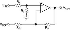
5.3. Noninverting Attenuation with Positive Offset
The case of noninverting attenuation with positive offset (Figure 5.2) is a minor variation of the noninverting attenuator, in this case, adding a second input for the reference, which is also attenuated by the voltage divider law.
 |
| Figure 5.2 Noninverting attenuation with positive offset: VOUT = mVIN + b, m = (1/R1)/(1/R1 + 1/R2 + 1/R3), b = VREF × (1/R3)/(1/R1 + 1/R2 + 1/R3). |
5.4. Noninverting Attenuation with Negative Offset
The case of noninverting attenuation with negative offset (Figure 5.3) is another slight variation of the noninverting buffer. In this case, instead of applying the reference by superposition to the noninverting input, the reference is applied to the inverting input through an inverting gain stage. The only limitation is that the gain on the reference must be equal to or greater than the stable bandwidth of the op amp.
 |
| Figure 5.3 Noninverting attenuation with negative offset: VOUT = mVIN – b, m = [R2/(R1 + R2)] × [1/(RF/RG)], b = VREF × (RF/RG). |
5.5. Inverting Attenuation with Zero Offset
This is the most often misdesigned circuit of all the cases. Many inexperienced designers create an unstable stage by attempting to extrapolate an inverting gain stage to the attenuation case by making RG greater than RF. The easiest fix for this problem is to use a voltage divider followed by a unity gain buffer, as described in Section 5.2. If inverting gain is absolutely required, then a similar solution can be implemented by adding a voltage divider to the input of an inverting gain stage.
The balance here is simple enough to understand, see Figure 5.4. RIN is split into RINA and RINB, the sum of which cannot be greater than RF. By the addition of RATTEN, the effective attenuation of the stage can be any value desired, while the gain of the stage from RINB and RF is always between a gain of 1 and 2.
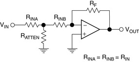 |
| Figure 5.4 Inverting attenuation with zero offset: VOUT = mVIN, m = (RF × RATTEN)/[RIN × (RIN + RATTEN)]. |
5.6. Inverting Attenuation with Positive Offset
If positive offset is needed along with inverting attenuation, a combination of the previous section and Section 5.2 can be employed (Figure 5.5). Just remember that the offset is also attenuated by the same factor as VIN.
 |
| Figure 5.5 Inverting attenuation with positive offset: VOUT = mVIN + b, m = (RF × RATTEN)/[RIN × (RIN + 2RATTEN)], b = VREF × [R2/(R1 + R2)] × [1 + RF/(RIN + RIN||RATTEN)]. |
5.7. Inverting Attenuation with Negative Offset
If negative offset is needed along with inverting attenuation, the reference can be added to the inverting input using a voltage summation method at the inverting input (Figure 5.6). Again, it is important to have a gain of more than 1 on the VREF gain channel or instability may result.
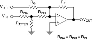 |
| Figure 5.6 Inverting unity gain with negative offset: VOUT = mVIN – b, m = (RF × RATTEN)/[RIN × (RIN + 2RATTEN)], b = VREF × RF/RG. |
5.8. Conclusion
The preceding circuits should provide a way to design just about any interface circuit the designer needs. The primary use of these gain and offset circuits, of course, is the interface between an input voltage and a data converter. The designer may also need to include filtering in their interface circuit, which is covered in later chapters.
..................Content has been hidden....................
You can't read the all page of ebook, please click here login for view all page.