
Chapter 11. Fully Differential Op Amps
11.1. Introduction
The term fully differential op amp probably brings chills to the spine of designers, with such thoughts as, “Oh no—now I have to learn something new.” What most designers don't realize is that, over 50 years ago, op amps began as fully differential components. Techniques about how to use the fully differential versions have been almost lost over the decades. Today's fully differential op amps offer performance advantages unheard of in those first units.
This chapter presents just the facts a designer needs to get started and some resources for further design assistance. We hope, after reading this chapter, a designer can approach a fully differential op amp design with confidence and excitement.
11.2. What Does Fully Differential Mean?
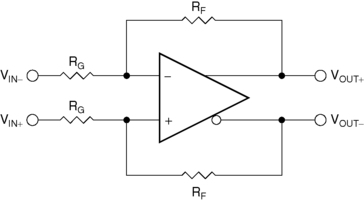
Designers should already be familiar with single ended op amps after reading the other chapters of this book. Briefly, single ended op amps (Figure 11.1) have two inputs, a positive input and negative input, which are understood to be fully differential. They have a single output, which is referenced to system ground.
| Figure 11.1 Single ended op amp schematic symbol. |
The op amp also has two power supply inputs, which are connected to bipolar power supplies (equal and opposite positive and negative potentials), or a single potential, with a positive supply and a ground connected to the power supply pins. These power supply pins are often omitted from the schematic symbol, when power supply connections are implied elsewhere on the schematic. Fully differential op amps add a second output, see Figure 11.2.
 |
| Figure 11.2 Fully differential op amp schematic symbol. |
The second output is fully differential, the two outputs are called positive output and negative output, similar terminology to the two inputs. Like the inputs, they are differential. The output voltages are equal but opposite in polarity (referenced to the common mode operating point of the circuit).
11.3. How Is the Second Output Used?
An op amp is used as a closed loop device. Most designers know how to close the loop on a single ended op amp (see Figure 11.3).
 |
| Figure 11.3 Closing the loop on a single ended op amp. |
Whether the single ended op amp is used in an inverting or a noninverting mode, the loop is closed from the output to the inverting input.
11.4. Differential Gain Stages
So, how is the loop closed on a fully differential op amp? It stands to reason, if there are two outputs, both have to be operated in closed loop form. Therefore, the equivalent way of closing the loop on a fully differential op amp is as shown in Figure 11.4.
 |
| Figure 11.4 Closing the loop on a fully differential op amp. |
Two identical feedback loops are required to close the loops for a fully differential op amp. If the loops are not matched, there can be significant second order harmonic distortion, but in some special cases, the output pathways can be different, and one such case is discussed later in this chapter.
Note that, for a fully differential op amp, each feedback loop is an inverting feedback loop. Both polarities of output are available, so terms like inverting and noninverting are meaningless. Instead, think of the single ended schematics in Figure 11.3. In both cases, the loop goes from the (noninverting) output to the inverting input, introducing a 180° phase shift. For the fully differential op amp, the top feedback loop has a 180° phase shift from the noninverting output to the inverting input, and the bottom feedback loop has a 180° phase shift from the inverting output to the noninverting input. Both feedback paths are therefore inverting. There is no “noninverting” fully differential op amp gain circuit.
The gain of the differential stage is
(11.1)
11.5. Single Ended to Differential Conversion
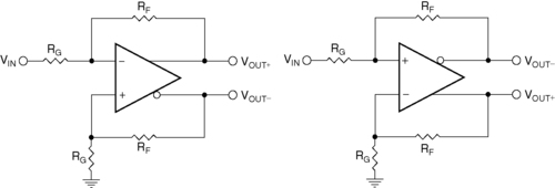
The schematic shown in Figure 11.4 is a fully differential gain circuit. Fully differential applications, however, are somewhat limited. Very often, the fully differential op amp is used to convert a single ended signal to a differential signal (Figure 11.5), perhaps to connect to the differential input of an analog to digital converter.
 |
| Figure 11.5 Single ended to differential conversion. |
The two configurations shown in Figure 11.5 are equivalent. At first glance, they look identical, but they are not. The difference is that, in the left configuration, the inverting input is used for signal and the noninverting input for reference. In the right configuration, the noninverting input is used for signal and the inverting input for reference. They are functionally equivalent—either one will work.
The gain of the single ended to differential stage is
(11.2)
The only difference between this configuration and the previous is that one side of the input voltage is referenced to ground.
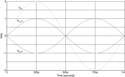
The dynamics of the gain are sometimes best described pictorially. Figure 11.6 shows the relationship among VIN, VOUT+, and VOUT− when RF = RG.
 |
| Figure 11.6 Relationship among VIN, VOUT+, and VOUT–. |
What is going on here? The amplitude of the input, VIN, is twice that of the output? The gain is correct, however, because the value of the differential gain, (VOUT+) − (VOUT−), at any point in Figure 11.6 is equal to the amplitude of VIN.
11.6. Working with Terminated Inputs
The design becomes more complicated if a single ended input signal must be terminated. This upsets the balance of the loop and changes the impedance. The design technique is anything but simple. Two equations in two variables interact, making design an interactive process. To simplify this difficult task for designers, Texas Instruments provides an online calculator on its Web site. This tool can be accessed through the Analog and Mixed-Signal Knowledgebase, by typing “fully differential component calculator” in the search text box.
The fully differential component calculator has six panes. Data entry is made primarily in the upper left pane, although the bottom middle pane contains some secondary entry fields.
The top middle pane contains the schematic for a terminated single ended to fully differential conversion. Design equations are shown in the upper right pane. The astute designer will see that the equations for RR3,R4 and Rt are interrelated through the A parameter. The tool makes a preliminary calculation to get close to the correct values, then it refines the calculation and “goal seeks” to the final value. The execution time depends on the step size used in the goal seeking calculation, and therefore selecting E96 resistor values execute much faster than Exact values. The designer should be patient, because execution times of several seconds or longer are possible, especially if gain is changed radically when Exact values is selected. The designer selects the desired gain and the impedance of the signal source (default value of 50 Ω). The designer then has the option of selecting a seed value for either R3 or R4 (but not both). If the designer attempts to select both, only the last value entered is used for calculation.
Almost without exception, the designer should initially try to select the value of R4, because it is often specified on the data sheet. The designer should experiment with R3 only if the recommended value of R4 does not yield an acceptable design (the tool has internal limits set to resistor values that make sense for real designs).
When the designer selects Calculate Values, the tool calculates resistor values in the bottom left pane and circuits simulation results in the bottom right pane. If the designer wishes, the power and input voltages can be changed in the bottom middle pane, and these affect the simulation results in the bottom right.
Note that this tool provides DC operating point only, it does not give AC simulation. Nevertheless, it saves the designer a lot of grief trying to do it using the “brute force” method.
11.7. A New Function
Texas Instruments' fully differential op amps have an additional pin, VOCM, which stands for “voltage output common mode (level).” The function of this pin can be either an input or an output, because its source is just a voltage divider off of the power supply—but it is seldom used as an output. When it is used as an output, it corresponds to the common mode voltage about which the VOUT+ and VOUT− outputs swing.
11.8. Conceptualizing the VOCM Input
Figure 11.7 and Figure 11.8 show electrical and mechanical models of VOCM, respectively.
 |
| Figure 11.7 Electrical model of VOCM. |
 |
| Figure 11.8 Mechanical model of VOCM. |
In the mechanical model, which is a more complex version of a child's teeter-totter, physically raising the VIN− arm (with a length of R1), causes the arm to pivot on fulcrum Vn, and the other side of the arm, VOUT+, to rise proportionally to the length of the arm (R2). A second fulcrum (VOCM), between the two arms, forces the end of the other arm (VOUT−) to go down by the same amount. The second arm also has a fulcrum at Vp, which causes its other side (VIN+) to move the same amount as VIN− but in the other direction (assuming lengths R1 = R3, and R2 = R4). VOCM can be used to raise and lower the average height (offset) of both VOUT+ and VOUT− equally. But, be careful! It can also exceed the mechanical limits of the model. Too low and the VOUT+ and VOUT− ends of the arms hit “ground.” Too high and the VIN− and VIN+ ends of the arms both hit “ground.” The base of the teeter-totter and its fulcrum represent the “potential” for movement or power supply.
We actually implemented this teeter-totter model with a well known set of child's building blocks, complete with a motor for excitation (Figure 11.9). The reader who has a set of these toys might consider building the model for some enjoyment, education, and a way to introduce children to the concepts of differential transmission.
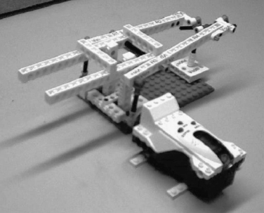 |
| Figure 11.9 A mechanical fully differential amplifier. |
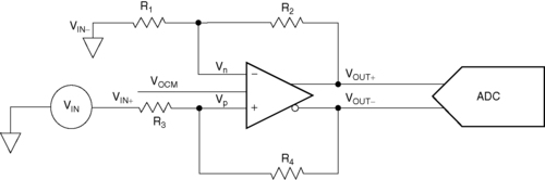
The most common use of the VOCM pin is to set the output common mode level of the fully differential op amp (Figure 11.10). This is a very useful function, because it can be used to match the common mode point of a data converter to which the fully differential amplifier is connected. High precision, high speed data converters often employ differential inputs and provide a reference output.
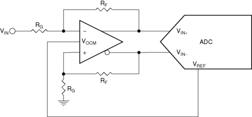 |
| Figure 11.10 Using a fully differential op amp to drive an ADC. |
The schematic of Figure 11.10 is simplified and does not show compensation, termination, or decoupling components for clarity. Nevertheless, it shows the basic concept. This is an important type of interface and is elaborated on further in a later chapter.
The remainder of this chapter presents the designer with a basic set of applications based on fully differential applications.
11.9. Instrumentation
An instrumentation amplifier can be constructed from two single ended amplifiers and a fully differential amplifier, as shown in Figure 11.11. Both polarities of the output signal are available, of course, and there is no ground dependence.
 |
| Figure 11.11 Instrumentation amplifier. |
11.10. Filter Circuits
Filtering is done to eliminate unwanted content in audio, among other things. Differential filters that do the same job to differential signals as their single ended cousins do to single ended signals can be applied.
For differential filter implementations, the components are simply mirror imaged for each feedback loop. The components in the top feedback loop are designated A, and those in the bottom feedback loop are designated B.
For clarity, decoupling components are not shown in the following schematics. Proper operation of high speed op amps requires proper decoupling techniques. That does not mean the shotgun approach of using inexpensive 0.1 μF capacitors. Decoupling component selection should be based on the frequencies that need to be rejected and the characteristics of the capacitors used at those frequencies.
11.10.1. Single Pole Filters
Single pole filters are the simplest filters to implement with single ended op amps, and the same holds true with fully differential amplifiers.
A low pass filter can be formed by placing a capacitor in the feedback loop of a gain stage, in a manner similar to single ended op amps (see Figure 11.12).
 |
| Figure 11.12 Single pole differential low pass filter. |
A high pass filter can be formed by placing a capacitor in series with an inverting gain stage as shown in Figure 11.13.
 |
| Figure 11.13 Single pole differential high pass filter. |
11.10.2. Double Pole Filters
Many double pole filter topologies incorporate positive and negative feedback and therefore have no differential implementation. Others employ only negative feedback but use the noninverting input for signal input and also have no differential implementation. This limits the number of options for designers, because both feedback paths must return to an input.
The good news, however, is that topologies are available to form differential low pass, high pass, bandpass, and notch filters. However, the designer might have to use an unfamiliar topology or more op amps than would have been required for a single ended circuit.
11.10.3. Multiple Feedback Filters
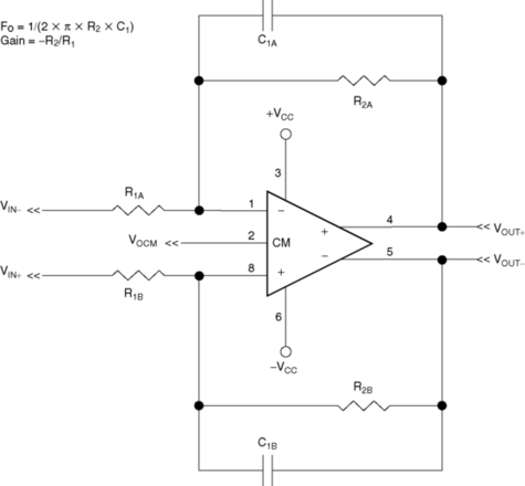
Multiple feedback (MFB) filter topology is the simplest topology that supports fully differential filters (Figure 11.14 and Figure 11.15). Unfortunately, the MFB topology is a bit hard to work with, but component ratios are shown for common unity gain filters.
 |
| Figure 11.14 Differential low pass filter. |
 |
| Figure 11.15 Differential high pass filter. |
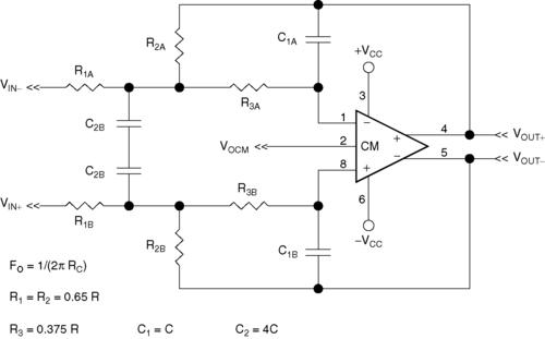
There is no reason why the feedback paths have to be identical. A bandpass filter can be formed by using nonsymmetrical feedback pathways (one low pass and one high pass). Figure 11.16 shows a bandpass filter that passes the range of human speech (300 Hz to 3 kHz). Figure 11.17 shows the response.
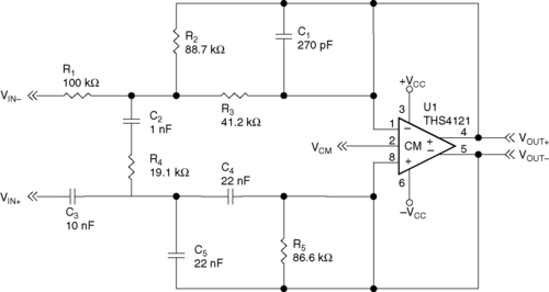 |
| Figure 11.16 Differential speech filter. |
 |
| Figure 11.17 Differential speech filter response. |
11.10.4. Biquad Filter
Biquad filter topology (Figure 11.18) is a double pole topology available in low pass, high pass, bandpass, and notch. The single ended implementation of this filter topology has three op amps, with the third op amp included only to invert the output of the previous op amp. That inversion is inherent in the fully differential op amp and therefore eliminates the third op amp, reducing the total number of op amps required to two.
 |
| Figure 11.18 Differential biquad filter. |
The high pass and notch versions of this particular biquad configuration require additional op amps, and therefore this topology is not optimum for them. Other topologies, however, can generate all four functions and can also be implemented with only two fully differential op amps.
..................Content has been hidden....................
You can't read the all page of ebook, please click here login for view all page.