
Chapter 12. Op Amp Noise Theory and Applications
Bruce Carter
12.1. Introduction
The purpose of op amp circuitry is the manipulation of the input signal in some fashion. Unfortunately, in the real world, the input signal has unwanted noise superimposed on it.
Noise is not something most designers get excited about. In fact, they probably wish the whole topic would go away. It can, however, be a fascinating study by itself. A good understanding of the underlying principles can, in some cases, be used to reduce noise in the design.
12.2. Characterization
Noise is a purely random signal, the instantaneous value or phase of the waveform cannot be predicted at any time. Noise can either be generated internally in the op amp or from its associated passive components or superimposed on the circuit by external sources. External noise is covered in another chapter and is usually the dominant effect.
12.2.1. rms versus P-P Noise
Instantaneous noise voltage amplitudes are as likely to be positive as negative. When plotted, they form a random pattern centered on zero. Since noise sources have amplitudes that vary randomly with time, they can be specified only by a probability density function. The most common probability density function is Gaussian. In a Gaussian probability function, there is a mean value of amplitude, which is most likely to occur. The probability that a noise amplitude will be higher or lower than the mean falls off in a bell shaped curve, which is symmetrical around the center (Figure 12.1).
 |
| Figure 12.1 Gaussian distribution of noise energy. |
The term σ is the standard deviation of the Gaussian distribution and the rms (root mean square) value of the noise voltage and current. The instantaneous noise amplitude is within ±1σ 68% of the time. Theoretically, the instantaneous noise amplitude can have values approaching infinity. However, the probability falls off rapidly as amplitude increases. The instantaneous noise amplitude is within ±3σ of the mean 99.7% of the time. If more or less assurance is desired, it is between ±2σ 95.4% of the time and ±3.4σ 99.94% of the time.
The term σ2 is the average mean square variation about the average value. This also means that the average mean square variation about the average value,  , is the same as the variance σ2.
Thermal noise and shot noise (see later) have Gaussian probability density functions. The other forms of noise do not.
12.2.2. Noise Floor
When all input sources are turned off and the output is properly terminated, a level of noise, called the noise floor, determines the smallest signal for which the circuit is useful. The objective for the designer is to place the signals that the circuit processes above the noise floor but below the level where the signals clip.
12.2.3. Signal to Noise Ratio
The noisiness of a signal is defined as
(12.1)
In other words, it is a ratio of signal voltage to noise voltage (hence the name signal to noise ratio).
12.2.4. Multiple Noise Sources
When there are multiple noise sources in a circuit, the total rms noise signal that results is the square root of the sum of the average mean square values of the individual sources:
(12.2)
Put another way, this is the only “break” the designer gets when dealing with noise. If the circuit contains two noise sources of equal amplitude, the total noise is not doubled (increased by 6 dB). It increases by only 3 dB. Consider a very simple case, two noise sources with amplitudes of 2 Vrms:
(12.3)
Therefore, with two equal sources of noise in a circuit, the noise is 20 × log(2.83/2) = 3.01 dB higher than if there were only one source of noise—instead of double (6 dB) as would be intuitively expected.
This relationship means that the worst noise source in the system tends to dominate the total noise. Consider a system in which one noise source is 10 Vrms and another is 1 Vrms:
(12.4)
There is hardly any effect from the 1 V noise source!
12.2.5. Noise Units
Noise is normally specified as a spectral density in rms volts or amps per root hertz,  or
or  . These are not very “user friendly” units. A frequency range is needed to relate these units to the actual noise levels that will be observed.
For example,
• A TLE2027 op amp with a noise specification of 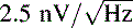 is used over an audio frequency range of 20 Hz to 20 kHz, with a gain of 40 dB. The output voltage is 0 dBV (1 V).
• To begin with, calculate the root hertz part:  .
.
• Multiply this by the noise spec, 2.5 × 141.35 = 353.38 nV, which is the equivalent input noise (EIN). The output noise equals the input noise multiplied by the gain, which is 100 (40 dB).
The signal to noise ratio can be now be calculated: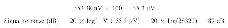
(12.5)
The TLE2027 op amp is an excellent choice for this application. Remember, though, that passive components and external noise sources can degrade performance. There is also a slight increase in noise at low frequencies, due to the 1/f effect (see later).
12.3. Types of Noise
Five types of noise are in op amps and their associated circuitry:
1 Shot noise
2 Thermal noise
3 Flicker noise
4 Burst noise
5 Avalanche noise
Some or all of these noises may be present in a design, presenting a noise spectrum unique to the system. It is not possible in most cases to separate the effects, but knowing general causes may help the designer optimize the design, minimizing noise in a particular bandwidth of interest. Proper design for low noise may involve a “balancing act” between these sources of noise and external noise sources.
12.3.1. Shot Noise
The name shot noise is short for Schottky noise, sometimes referred to as quantum noise. It is caused by random fluctuations in the motion of charge carriers in a conductor. Put another way, current flow is not a continuous effect. Current flow is electrons, charged particles that move in accordance with an applied potential. When the electrons encounter a barrier, potential energy builds until they have enough energy to cross that barrier. When they have enough potential energy, it is abruptly transformed into kinetic energy as they cross the barrier. A good analogy is stress in an earthquake fault that is suddenly released as an earthquake.
As each electron randomly crosses a potential barrier, such as a pn junction in a semiconductor, energy is stored and released as the electron encounters and then shoots across the barrier. Each electron contributes a little pop as its stored energy is released when it crosses the barrier (Figure 12.2).
 |
| Figure 12.2 Shot noise generation. |
The aggregate effect of all of the electrons shooting across the barrier is the shot noise. Amplified shot noise has been described as sounding like lead shot hitting a concrete wall.
Some characteristics of shot noise are these:
• Shot noise is always associated with current flow. It stops when the current flow stops.
• Shot noise is independent of temperature.
• Shot noise is spectrally flat or has a uniform power density, meaning that when plotted versus frequency it has a constant value.
• Shot noise is present in any conductor—not just a semiconductor. Barriers in conductors can be as simple as imperfections or impurities in the metal. The level of shot noise, however, is very small due to the enormous numbers of electrons moving in the conductor and the relative size of the potential barriers. Shot noise in semiconductors is much more pronounced.
The rms shot noise current is equal to where
where
(12.6)
q = Electron charge (1.6 × 12–19 coulombs).
IDC = Average forward DC current in amps.
IQ = Reverse saturation current in amps.
B = Bandwidth in hertz.
If the pn junction is forward biased, IO is zero, and the second term disappears. Using Ohm's law and the dynamic resistance of a junction,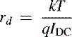
(12.7)
The rms shot noise voltage is equal to where
where
(12.8)
k = Boltzmann's constant (1.38 × 10⁻²³ joules/K).
q = Electron charge (1.6 × 12−19 coulombs).
T = Temperature in Kelvins.
IDC = Average DC current in amps.
B = Bandwidth in hertz.
For example, a junction carries a current of 1 mA at room temperature. Its noise over the audio bandwidth is Obviously, it is not much of a problem in this example.
(12.9)
Look closely at the formula for shot noise voltage. Note that the shot noise voltage is inversely proportional to the current. Stated another way, shot noise voltage decreases as average DC current increases and increases as average DC current decreases. This can be an elegant way of determining if shot noise is a dominant effect in the op amp circuit being designed. If possible, decrease the average DC current by a factor of 100 and see if the overall noise increases by a factor of 10. In the preceding example, The shot noise voltage does increase by a factor of 10, or 20 dB.
(12.10)
12.3.2. Thermal Noise
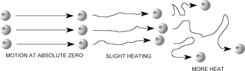
Thermal noise is sometimes referred to as Johnson noise, after its discoverer. It is generated by thermal agitation of electrons in a conductor. Simply put, as a conductor is heated, it becomes noisy. Electrons are never at rest; they are always in motion. Heat disrupts the electrons' response to an applied potential. It adds a random component to their motion (Figure 12.3). Thermal noise stops only at absolute zero.
 |
| Figure 12.3 Thermal noise. |
Like shot noise, thermal noise is spectrally flat or has a uniform power density (it is white), but thermal noise is independent of current flow.
At frequencies below 100 MHz, thermal noise can be calculated using Nyquist's relation: or
or where
where
(12.11)
(12.12)
ETH = Thermal noise voltage in volts rms.
ITH = Thermal noise current in amps rms.
k = Boltzmann's constant (1.38 × 10⁻²³).
T = Absolute temperature (in Kelvins).
R = Resistance in ohms.
B = Noise bandwidth in hertz (fMAX – fMIN).
The noise from a resistor is proportional to its resistance and temperature. It is important not to operate resistors at elevated temperatures in high gain input stages. Lowering resistance values also reduces thermal noise.
For example, the noise in a 100 kΩ resistor at 25°C (298 K) over the audio frequency range of 20 Hz to 20 kHz is
(12.13)
Decreasing the temperature would reduce the noise slightly, but scaling the resistor down to 1 kΩ (a factor of 100) would reduce the thermal noise by 20 dB. Similarly, increasing the resistor to 10 MΩ would increase the thermal noise to –84.8 dBV, a level that would affect a 16 bit audio circuit. The noise from multiple resistors adds according to the root mean square law in Section 12.2.4. Beware of large resistors used as the input resistor of an op amp gain circuit, their thermal noise is amplified by the gain in the circuit (Section 12.4). Thermal noise in resistors is often a problem in portable equipment, where resistors have been scaled up to get power consumption down.
12.3.3. Flicker Noise
Flicker noise is also called 1/f noise. Its origin is one of the oldest unsolved problems in physics. It is pervasive in nature and in many human endeavors. It is present in all active and many passive devices. It may be related to imperfections in crystalline structure of semiconductors, as better processing can reduce it.
Some characteristics of flicker noise are these: where
where
• It increases as the frequency decreases, hence the name 1/f.
• It is associated with a DC current in electronic devices.
• It has the same power content in each octave (or decade).
(12.14)
Ke and Ki are proportionality constants (volts or amps) representing En and In at 1 Hz.
fMAX and fMIN are the minimum and maximum frequencies in hertz.
Flicker noise is found in carbon composition resistors, where it is often referred to as excess noise, because it appears in addition to the thermal noise that is there. Other types of resistors also exhibit flicker noise to varying degrees, with wire wound showing the least. Since flicker noise is proportional to the DC current in the device, if the current is kept low enough, thermal noise will predominate and the type of resistor used will not change the noise in the circuit.
Reducing power consumption in an op amp circuit by scaling up resistors may reduce the 1/f noise, at the expense of increased thermal noise.
12.3.4. Burst Noise
Burst noise, also called popcorn noise, is related to imperfections in semiconductor material and heavy ion implants. It is characterized by discrete high frequency pulses. The pulse rates may vary, but the amplitudes remain constant at several times the thermal noise amplitude. Burst noise makes a popping sound at rates below 100 Hz when played through a speaker—it sounds like popcorn popping, hence the name. Low burst noise is achieved by using clean device processing and therefore is beyond the control of the designer. Modern processing techniques at Texas Instruments have all but eliminated its occurrence.
12.3.5. Avalanche Noise
Avalanche noise is created when a pn junction is operated in the reverse breakdown mode. Under the influence of a strong reverse electric field within the junction's depletion region, electrons have enough kinetic energy that, when they collide with the atoms of the crystal lattice, additional electron/hole pairs are formed (Figure 12.4). These collisions are purely random and produce random current pulses similar to shot noise but much more intense.
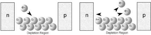 |
| Figure 12.4 Avalanche noise. |
When electrons and holes in the depletion region of a reversed biased junction acquire enough energy to cause the avalanche effect, a random series of large noise spikes is generated. The magnitude of the noise is difficult to predict due to its dependence on the materials.
Because the zener breakdown in a pn junction causes avalanche noise, it is an issue with op amp designs that include zener diodes. The best way of eliminating avalanche noise is to redesign a circuit to use no zener diodes.
12.4. Noise Colors
While the noise types are interesting, real op amp noise appears as the summation of some or all of them. The various noise types themselves are difficult to separate. Fortunately, there is an alternative way to describe noise, called color. The colors of noise come from rough analogies to light and refer to the frequency content. Many colors are used to describe noise, some of them having a relationship to the real world and some of them more attuned to the field of psychoacoustics.
White noise is in the middle of a spectrum that runs from purple to blue to white to pink and red/brown. These colors correspond to powers of the frequency to which their spectrum is proportional, as shown in Table 12.1.
An infinite number of variations lie between the colors. All inverse powers of frequency are possible, as are noises that are narrowband or appear only at one discrete frequency. Those, however, are primarily external sources of noise, so their presence is an important clue that the noise is external, not internal. There are no pure colors; at high frequencies, all of them begin to roll off and become pinkish. The op amp noise sources just described appear in the region between white noise and red/brown noise (Figure 12.5).
 |
| Figure 12.5 Noise colors. |
12.4.1. White Noise
White noise is noise in which the frequency and power spectrum is constant and independent of frequency. The signal power for a constant bandwidth (centered at frequency fO) does not change if fO is varied. Its name comes from a similarity to white light, which has equal quantities of all colors.
When plotted versus frequency, white noise is a horizontal line of constant value.
Shot and thermal (Johnson) noise sources are approximately white, although there is no such thing as pure white noise. By definition, white noise would have infinite energy at infinite frequencies. White noise always becomes pinkish at high frequencies.
Steady rainfall or radio static on an unused channel approximate a white noise characteristic.
12.4.2. Pink Noise
Pink noise is noise with a 1/f frequency and power spectrum excluding DC. It has equal energy per octave (or decade for that matter). This means that the amplitude decreases logarithmically with frequency. Pink noise is pervasive in nature—many supposedly random events show a 1/f characteristic.
Flicker noise displays a 1/f characteristic, which also means that it rolls off at 3 dB/octave.
12.4.3. Red/Brown Noise
Red noise is not universally accepted as a noise type. Many sources omit it and go straight to brown, attributing red characteristics to brown. This has more to do with aesthetics than anything else (if brown noise is the low end of the spectrum, then pink noise should be named tan). So if pink noise is pink, then the low end of the spectrum should be red. Red noise is named for a connection with red light, which is on the low end of the visible light spectrum. But then, this noise simulates Brownian motion, so perhaps it should be called Brown. Red/brown noise has a –6 dB/octave frequency response and a frequency spectrum of 1/f2 excluding DC.
Red/brown noise is found in nature. The acoustic characteristics of large bodies of water approximate red/brown noise frequency response.
Popcorn and avalanche noise approximate a red/brown characteristic, but they are more correctly defined as pink noise, where the frequency characteristic has been shifted down as far as possible in frequency.
12.5. Op Amp Noise
This section describes the noise in op amps and associated circuits.
12.5.1. The Noise Corner Frequency and Total Noise
Op amp noise is never specified as shot, thermal, or flicker, or even white or pink. Noise for audio op amps is specified with a graph of equivalent input noise versus frequency.
These graphs usually show two distinct regions:
• Lower frequencies where pink noise is the dominant effect.
• Higher frequencies where white noise is the dominant effect.
Actual measurements for the TLV2772 show that the noise has both white and pink characteristics (Figure 12.6). Therefore, the noise equations for each type of noise cannot approximate the total noise out of the TLV2772 over the entire range shown on the graph. It is necessary to break the noise into two parts—the pink part and the white part—then add those parts together to get the total op amp noise using the root mean square law of Section 12.2.4.
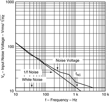 |
| Figure 12.6 TLV2772 op amp noise characteristics. |
12.5.2. The Corner Frequency
The point in the frequency spectrum where 1/f noise and white noise are equal is referred to as the noise corner frequency, fNC. Note on the graph in Figure 12.6 that the actual noise voltage is higher at fNC due to the root mean square addition of noise sources, as defined in Section 12.2.4.
The value of fNC can be determined visually from the graph in Figure 12.6. It appears a little above 1 kHz. This was done by
• Taking the white noise portion of the curve and extrapolating it down to 10 Hz as a horizontal line.
• Taking the portion of the pink noise from 10 Hz to 100 Hz and extrapolating it as a straight line.
• The point where the two intercept is fNC, the point where the white noise and pink noise are equal in amplitude. The total noise is then  white noise specification (from Section 10.2.4). This would be about
 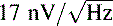 for the TLV2772.
This is good enough for most applications. As can be seen from the actual noise plot in Figure 12.6, small fluctuations make precise calculation impossible. There is a precise method, however:
• Determine the 1/f noise at the lowest possible frequency.
• Square it.
• Subtract the white noise voltage squared (subtracting noise with root mean squares is just as valid as adding).
• Multiply by the frequency. This will give the noise contribution from the 1/f noise.
• Then, divide by the white noise specification squared. The answer is fNC.
For example, the TLV2772 has a typical noise voltage of  at 10 Hz (from a 5 V plot on a data sheet).
The typical white noise specification for the TLV2772 is 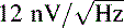 (from the data sheet) is
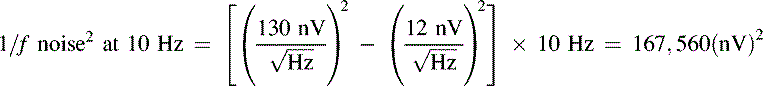
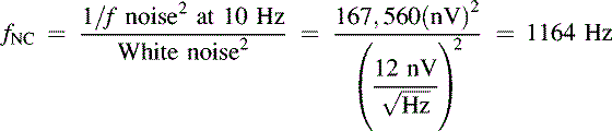
(12.15)
(12.16)
Once the corner frequency is known, the individual noise components can be added together as shown in Section 12.2.2. Continuing the preceding example for a frequency range of 10 Hz to 10 kHz,

(12.17)
(12.18)
This example presupposed that the bandwidth includes fNC. If it does not, all of the contribution is from either the 1/f noise or the white noise. Similarly, if the bandwidth is very large and extends to three decades or so above fNC, the contribution of the 1/f noise can be ignored.
12.5.3. The Op Amp Circuit Noise Model
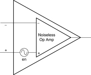
Texas Instruments measures the noise characteristics of a large sampling of devices. This information is compiled and used to determine the typical noise performance of the device. These noise specifications refer the input noise of the op amp. Some noise portions can be represented better by a voltage source and some by a current source. Input voltage noise is always represented by a voltage source in series with the noninverting input. Input current noise is always represented by current sources from both inputs to ground (Figure 12.7).
 |
| Figure 12.7 Op amp circuit noise model. |
In practice, op amp circuits are designed with low source impedance on the inverting and noninverting inputs. For low source impedances and CMOS JFET inputs, only the noise voltage is important; the current sources are insignificant in the calculations because they are swamped in the input impedances.
The equivalent circuit, therefore, reduces to that shown in Figure 12.8.
 |
| Figure 12.8 Equivalent op amp circuit noise model. |
12.5.4. Inverting Op Amp Circuit Noise
If the previous circuit is operated in an inverting gain stage, the equivalent circuit becomes that shown in Figure 12.9.
 |
| Figure 12.9 Inverting op amp circuit noise model. |
The additional voltage sources e1 through e3 represent the thermal noise contribution from the resistors. As stated in Section 12.3.2, the resistor noise can also be discounted if the values are low. Resistor noise is omitted in the examples that follow. R3 is also not usually present, unless low common mode performance is important. Deleting it and connecting the noninverting input directly to (virtual) ground makes the common mode response of the circuit worse but may improve the noise performance of some circuits. This means one less noise source to worry about. Therefore, the equivalent circuit becomes that shown in Figure 12.10.
 |
| Figure 12.10 Inverting equivalent op amp circuit noise model. |
This simplifies the gain calculation: where en = the total noise over the bandwidth of interest.
(12.19)
12.5.5. Noninverting Op Amp Circuit Noise
Taking the simplified equivalent op amp circuit from Section 12.5.2 as the base, the noise equivalent of a noninverting op amp circuit is shown in Figure 12.11.
 |
| Figure 12.11 Noninverting equivalent op amp circuit noise model. |
The gain of this circuit is
(12.20)
12.5.6. Differential Op Amp Circuit Noise Model
Taking the simplified equivalent op amp circuit from Section 12.5.2 as the base, the noise equivalent of a differential op amp circuit is shown in Figure 12.12.
 |
| Figure 12.12 Differential equivalent op amp circuit noise model. |
Assuming that R1 = R3 and R2 = R4, the gain of this circuit is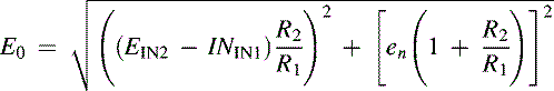
(12.21)
12.5.7. Summary
The previous examples, though trivial, illustrate that noise always adds to the overall output of the op amp circuit. Reference [1] provides a much more in-depth derivation of op amp noise in circuits, including resistive effects.
12.6. Putting It All Together
This example is provided for analysis only—actual results depend on a number of other factors. Expanding on the techniques of Section 12.2.5, a low noise op amp is needed over an audio frequency range of 20 Hz to 20 kHz, with a gain of 40 dB. The output voltage is 0 dBV (1 V). The schematic is shown in Figure 12.13.
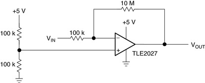 |
| Figure 12.13 Split supply op amp circuit. |
It would be nice to use a TLE2027, with a noise figure of  . The data sheet, however, reveals that this is a ±15 V part and that noise figure is specified at only ±15 V. Furthermore, the specification for VOM+ and VOM– (see Chapter 13) shows that it can swing to only within approximately 2 V of its voltage rails. If they are +5 V and ground, the op amp is close to clipping with a 1 V output signal. This illustrates a common fallacy: The designer chooses an op amp based on one parameter only, without checking others that affect the circuit. An expert analog designer must develop an attention to details or be prepared to spend a lot of time in the lab with false starts and unexpected problems.
So, the only choice is to select a different op amp. The TLC2201 is an excellent choice. It is a low noise op amp optimized for single supply operation.
The first circuit change in this example is to change the TLE2027 to a TLC2201. Visually, the corner frequency, fNC, appears to be somewhere around 20 Hz (from Section 12.5.2), the lower frequency limit of the band we are interested in. This is good: It means, for all practical purposes, the 1/f noise can be discounted. It has  noise instead of
  , and from Section 12.2.5,
• To begin with, calculate the root hertz part: 
• Multiply this by the noise spec, 8 × 141.35 = 1.131 μV, which is the equivalent input noise. The output noise equals the input noise multiplied by the gain, which is 100 (40 dB).
The signal to noise ratio can be now be calculated:
(12.22)
Pretty good, but it is 10 dB less than would have been possible with a TLE2027. If this is not acceptable (let's say for 16 bit accuracy), you are forced to generate a ±15 V supply. Suppose for now that 78.9 dB signal to noise is acceptable, and build the circuit.
When it is assembled, it oscillates. What went wrong?
To begin with, it is important to look for potential sources of external noise. The culprit is a long connection from the half supply voltage reference to the high impedance noninverting input. Added to that is a source impedance that does not effectively swamp external noise sources from entering the noninverting input. There is a big difference between simply providing a correct DC operating point and providing one that has low impedances where they are needed. Most designers know the “fix,” which is to decouple the noninverting input, as shown in Figure 12.14.
 |
| Figure 12.14 TLC2201 op amp circuit. |
Better—it stopped oscillating. Probably a nearby noise source radiating into the noninverting input was providing enough noise to put the circuit into oscillation. The capacitor lowers the input impedance of the noninverting input and stops the oscillation. Much more information on this topic is found in Chapter 23, including layout effects and component selection. For now, it is assumed that all of these have been taken into account.
The circuit is still slightly noisier than the 78.9 dB signal to noise ratio given previously, especially at lower frequencies. This is where the real work of this example begins, that of eliminating component noise.
The circuit in Figure 12.15 has four resistors. Assuming that the capacitor is noiseless (not always a good assumption), that means four noise sources. For now, only the two resistors in the voltage divider that forms the voltage reference are considered. The capacitor, however, has transformed the white noise from the resistors into pink (1/f) noise. From 12.3.2 and 12.2.5, the noise from the resistors and the amplifier itself is

(12.23)
(12.24)
 |
| Figure 12.15 Improved TLC2201 op amp circuit. |
So far, so good. The amplifier noise is swamping the resistor noise, which only adds a very slight pinkish component at low frequencies. Remember, however, that this noise voltage is multiplied by 101 through the circuit, but that was previously taken into account for the preceding 78.9 dB signal to noise calculation.
Reducing the value of the resistors to decrease their noise is an option. Changing the voltage divider resistors from 100 kΩ to 1 kΩ while leaving the 0.1 μV capacitor the same changes the corner frequency from 32 Hz to 796 Hz, right in the middle of the audio band.
Note: Resist the temptation to make the capacitor larger to move the pinkish effect below the lower limits of human hearing. The resulting circuit must charge the large capacitor up during power up and down during power down. This may cause unexpected results.
If the noise from the half supply generator is critical, the best possible solution is to use a low noise, low impedance half supply source. Remember, however, that its noise is multiplied by 101 in this application.
The effect of the 100 kΩ resistor on the inverting input is whitish and appears across the entire bandwidth of the circuit. Compared to the amplifier noise, it is still small, just like the noise from the noninverting resistors on the input. The noise contribution of resistors is discounted.
Of much more concern, however, is the 10 MΩ resistor used as the feedback resistor. The noise associated with it appears as a voltage source at the inverting input of the op amp and, therefore, is multiplied by a factor of 100 through the circuit. From Section 12.3.2, the noise of a 10 MΩ resistor is –84.8 dBV, or 57.3 μV. Adding this and the 100 kΩ resistor noise to the amplifier noise,

(12.25)
(12.26)
The noise contribution from the 10 MΩ resistor subtracts 1 dB from the signal to noise ratio. Changing the 10 MΩ resistor to 100 kΩ and the input resistor from 100 kΩ to 1 kΩ preserves the overall gain of the circuit. The redesigned circuit is shown in Figure 12.15.
For frequencies above 100 Hz, where the 1/f noise from the op amp and the reference resistors is negligible, the total noise of the circuit is

(12.27)
(12.28)
Proper selection of resistors, therefore, has yielded a signal to noise ratio close to the theoretical limit for the op amp itself. The power consumption of the circuit, however, has increased slightly, which may be unacceptable in a portable application. Remember, too, that this signal to noise ratio is only at an output level of 0 dBV, an input level of –40 dBV. If the input signal is reduced, the signal to noise ratio is reduced proportionally.
Music, in particular, almost never sustains peak levels. The average amplitude may be down 20 dB to 40 dB from the peak values. This erodes a 79 dB signal to noise ratio to 39 dB in quiet passages. If someone “cranks up the volume” during the quiet passages, the noise becomes audible. This is done automatically with automatic volume controls. The only way a designer can combat this is to increase the voltage levels through the individual stages. If the preceding audio stages connecting to this example, for instance, could be scaled to provide 10 dB more gain, the TLC2201 would be handling an output level of 3.16 V instead of 1 V, which is well within its rail to rail limit of 0 V to 4.7 V. This would increase the signal to noise gain of this circuit to 88.9 dB, almost the same as would have been possible with a TLE2027 operated off of ±15 V! But noise in the preceding stages would also increase. Combatting noise is a difficult problem, and trade-offs are always involved.
Reference
1. Texas Instruments Application Report, Noise Analysis in Operational Amplifier Circuits. (1999) ; SLVA043A.
..................Content has been hidden....................
You can't read the all page of ebook, please click here login for view all page.