
Chapter 14. Instrumentation
Sensors to A/D Converters
Ron Mancini
14.1. Introduction
The typical transducer measurement system block diagram is shown in Figure 14.1. The transducer is the electronic system's interface with the real world, and it issues data about a variable. The transducer converts the data into an electrical signal adequate for processing by the circuitry that follows the transducer. Bias and excitation circuitry does the care and feeding of the transducer, providing the offset voltages, bias currents, excitation signals, external components, and protection required for the transducer to operate properly. The output of the transducer is an electrical signal representing the measured variable.
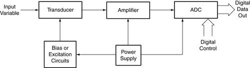 |
| Figure 14.1 Block diagram of a transducer measurement system. |
The variables that must be measured are determined by the customer's application, and the measured variable normally dictates the transducer selection. If the measured variable is temperature, then some sort of temperature sensing transducer must be employed and the range of temperatures to be measured or the accuracy of the measurement is the primary factor influencing temperature transducer selection. Note that the electrical output of the transducer is not a major concern at this point in the transducer selection. The transducer's electrical output is always a consideration, although picking the right transducer for the job is the primary goal. The correct transducer for the job can have an ohm per degree Centigrade change, microvolt per degree Centigrade change, or millivolt per degree Centigrade change. All transducers have offset voltages or currents, and they can be referenced to ground, either power supply rail, or some other voltage. The selection of the transducer is out of circuit designer's hands; therefore the circuit designer must accept what the application demands.
The A/D converter (ADC) selection is based on several system criteria, such as resolution, conversion speed, power requirements, physical size, processor compatibility, and interface structure. The ADC must have enough bits to obtain the resolution required by the accuracy specification. The formula for calculating the resolution of an ADC is given in Equation (14.1), where n is the number of significant bits contained in the ADC:
(14.1)
Some confusion exists about the word bits, because the same word is used for binary bits and significant bits. Binary bits are ones and zeros used to calculate binary numbers; for example, a converter with eight digital states has significant bits and 2n = 256 binary bits (see Figure 14.2). The voltage value of a single bit, called a least significant bit (LSB), is calculated in Equation (14.2):
(14.2)
 |
| Figure 14.2 Significant bits versus binary bits. |
FSV is the full scale voltage of the converter in volts; hence, a 14 bit converter FSV = 10 V has an LSB equal to 10/212 = 2.441406 mV/bit. In an ADC, an LSB is the maximum voltage change required to for a 1 bit output change; and in an ADC, an LSB is defined as LSB = FSV/(2n − 1).
Conversion speed is not critical in temperature measurement applications, because temperature changes occur at slow rates. Directional control in a rocket traveling at Mach 2 happens much faster than temperature changes, so conversion speed is an important factor in rocket applications. The speed of an ADC is generally thought of as the conversion time plus the time required between conversions, and conversion speed dictates the converter structure. When conversion speed is a primary specification, a flash converter is used, and flash converters require low impedance driving circuits. This is an example of a converter imposing a specification requirement, low output impedance, on the driving amplifier.
The system definition specifies the voltages available for design and the maximum available current drain. Some systems have multiple voltages available, and others are limited to a single voltage. The available voltage affects the converter selection. Size, processor compatibility, and interface structure are three more factors that must be considered when selecting the ADC. The available package that the converter comes in determines what footprint or size the converter takes on the printed circuit board. Some applications preclude large, power hungry ADCs, so these applications are limited to recursive or ∑Δ type ADCs. The converter must be compatible with the processor to preclude the addition of glue logic; so the processor dictates the ADC's structure. This defines the interface structure, sometimes the ADC structure, and the ADC timing.
Note that the amplifier designer has not been consulted during this decision process, but, in actuality, the systems engineers do talk to the amplifier designers, if only to pacify them. The selection of the ADC is out of the circuit designer's hands; so the circuit designer must accept what the application demands.
Many different transducer/ADC combinations are possible, and each combination has a different requirement. Although they may be natural enemies, any transducer may be coupled with any ADC, therefore the amplifier must make the coupling appear to be seamless. There is no reason to expect that the selected transducer's output voltage span matches the selected ADC's input voltage span, so an amplifier stage must match the transducer output voltage span to the ADC input voltage span. The amplifier stage amplifies the transducer output voltage span and shifts its DC level until the transducer output voltage span matches the ADC input voltage span. When the spans are matched, the transducer/ADC combination achieves the ultimate accuracy; any other condition sacrifices accuracy or dynamic range.
The transducer output voltage span seldom equals the ADC input voltage span. Transducer data are lost or the ADC dynamic range is not fully utilized when the spans are unequal, start at different DC voltages, or both. In Figure 14.3(A), the spans are equal (3 V), but they are offset by 1 V. This situation requires level shifting to move the sensor output voltage up by 1 V so the spans match. In Figure 14.3(B), the spans are unequal (2 V and 4 V), but no offset voltage exists. This situation requires amplification of the sensor output to match the spans. When the spans are unequal (2 V versus 3 V) and offset (1 V), as is the case in Figure 14.3(C), level shifting and amplification are required to match the spans.
 |
| Figure 14.3 Example of spans that require correction. |
The output span of the transducer must be matched to the input span of the ADC to achieve optimum performance. When the spans are mismatched, either the transducer output voltage does not fit into the ADC input span, hence losing sensor data, or the transducer output voltage does not fill the ADC input span, losing ADC accuracy. The latter situation requires an increase in ADC dynamic range (increased cost), because a higher bit converter must be used to achieve the same resolution. The best analog circuit available for matching the spans is the op amp because it level shifts and amplifies the input voltage to make the spans equal. The op amp is so versatile that it shifts the signal's DC level and amplifies the input signal simultaneously.
A similar but different problem exists in the digital to analog converter (DAC) to actuator interface. The DAC output voltage or current span must match the actuator input voltage span to achieve maximum performance. The procedure for matching the DAC output span to the actuator input span can be quite different from the procedure for matching the transducer output span to the ADC input span. Transducer outputs are usually low level signals, so care must be taken to preserve their signal to noise ratio. Actuator input signals may require significant power, so robust op amps are required to drive some actuators.
The system specifications eventually determine the transducer, ADC, and analog circuit specifications. System specifications are seen as absolute specifications; they must be met for the design to function in a satisfactory manner. Component specifications are divided into several categories; absolute maximum ratings (AMRs), guaranteed minimum/maximum specifications (VMAX or VMIN), typical specifications (V), and guaranteed but not tested (GNT) specifications.
If any of the device parameters is taken beyond the AMR, the device can be destroyed (expect destruction). The manufacturer guard bands the AMR to guarantee safety and quality, and you should guard band the AMRs, too. Typical specifications are the most appealing, but throw them out because they are meaningless in most cases. In the vast majority of cases, the typical specifications are not related to meaningful data; rather, they are marketing dreams. Never design with typical specifications unless you are in the habit of designing with meaningless data or have a good reason for believing that the typical specification is close to reality. A violation of this rule is a specification, like output voltage swing, that depends heavily on test conditions, such as the value of the load resistor. When the load resistance is much higher than that specified for the test condition, the output voltage swing is closer to the typical specification rather than the guaranteed specification. The laws of physics guarantee this truth, but the amount of extra voltage swing achieved is hard to calculate.
Guaranteed minimum/maximum specifications define the limits of a parameter. The parameter always exceeds the minimum value and it never exceeds the maximum value. The guaranteed min/max specifications are your design specifications. Guaranteed but not tested specifications are usually applied to parameters that are very expensive to test. The manufacturer either tests some other parameter related to the specification or it sample tests each lot to ensure compliance. GNT specifications are design specifications. There is a fifth specification, called guaranteed by design (GBD); and if they are not critical specifications, GBD is a useful design specification.
All specifications have conditions associated with testing. They specify ambient temperature, supply voltage, test signals, test loads, and other conditions; and they define how the measurements are made. Inspect the test conditions carefully; an op amp that specifies a 5 V output swing with a 50 Ω load is much more capable of driving a load than an op amp that specifies a 5 V output swing with a 10 kΩ load. Beware, you assume the risk of a parameter being out of specification when you use devices at conditions other than the test conditions.
An error budget is a logical and orderly method of tabulating errors, and it helps the designer keep track of the errors by error sources. Meeting the system specifications translates into minimizing errors, choosing components with acceptable errors and canceling or eliminating errors when possible. The error budget is first applied to the ADC and transducer because they are the components over which the designer has the least control. When these two error budgets are combined and subtracted from the system error allowance, the result is the error allowance for the amplifier and peripheral circuits. The designer must choose components and design wisely to stay within the error allowance, or the system specifications are not met.
Sometimes the systems specifications can't be met, and this fact is greeted with moans, name calling, and finger pointing. The error budgets are the design engineer's only defense against subjective accusations. The error budgets document the design trail, and they show where changes need to be made to do the best job possible. It is very hard to maintain an error budget, because errors must be converted to equivalent units (volts, bits, or amps) and the impact of the error term may not be calculable at that point in the design. When this situation occurs, tabulate the error terms in a table and calculate their effect later in the design process.
This chapter teaches the designer how to characterize the transducer and ADC, how to determine amplifier and design specifications through the use of error budgets, and how to complete circuit design. The equations developed in this chapter are not nearly as important as the design philosophy.
14.2. Transducer Types
This is not a treatise on transducers, but an appreciation for the many types of transducers gives a feel for the extent and complexity of the transducer characterization problem (following section). The variety of electrical output that they offer loosely groups transducers. Various types of transducer outputs are resistive, optical, AC excited, junction voltage, and magnetic; and each of these outputs must be converted to an electrical signal that can be amplified to fit the input span of an ADC. There are excellent references (such as [1]) that deal with transducer characterization, but the transducer manufacturer should be your first source of reference material.
Transducer manufacturers publish data similar to that contained in an IC data sheet, and they take the same liberties with typical specifications as the IC manufacturers. Sort through the data to determine the meaning of the various specifications, then pay special attention to the test conditions that prevailed when the data were gathered. Look for application notes that show transducer excitation, bias, or interface circuits. Search several manufacturers for similar information because nobody manages to cover every aspect of a design.
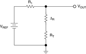
Some transducers, such as strain gauges, thermistors, RTDs, and potentiometers, sense a change in resistance (ΔR). The ΔR sensing devices are used in at least three circuit configurations: the voltage divider, current excited, and Wheatstone bridge circuits shown in Figure 14.4Figure 14.5 and Figure 14.6. The transducer resistance is RT, and the change in transducer resistance caused by a change in the measured variable is ΔR.
 |
| Figure 14.4 Voltage divider circuit for a resistive transducer. |
 |
| Figure 14.5 Current source excitation for a resistive transducer. |
 |
| Figure 14.6 Precision current source. |
The voltage divider circuit uses a stable reference voltage to convert the transducer resistance into voltage, and its output voltage is given in Equation (14.3):
(14.3)
If R1 is comparable in value to RT, the circuit has very low sensitivity because the circuit must measure a small change in resistance in the presence of a large resistance. When the bias resistor, R1, is selected as a large value, VREF and R1 act as a current source and the transducer resistance can be neglected in the calculations, yielding Equation (14.4). When R1 ≫ (RT + ΔR) Equation (14.3) reduces to Equation (14.4):
(14.4)
Equation (14.5) is the equivalent of Equation (14.4) and it is obtained by exciting the transducer with a bias current as shown in Figure 14.5. The bias current can be made very accurate by employing op amps in a current source configuration, as shown in Figure 14.6; therefore the approximation R1 ≫ (RT + ΔR) need not enter the calculations: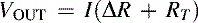
(14.5)
The Wheatstone bridge shown in Figure 14.7 is a precision device used to measure small changes in resistance. One leg of the bridge is made up of a voltage divider consisting of equal stable resistors (R1 and R2) and the reference voltage. When RX and ΔR equal zero, RTX is selected equal to RT. As the transducer resistance changes, ΔR assumes some value, and RX is switched until the bridge output voltage nulls to zero. At this point, the value of ΔR is read from the RX dial. Bridge circuits are used to convert resistive transducer values to dial readings, but some methods of using transducers in bridge circuits yield a voltage change proportional to the resistance change. The bridge circuit has a high output impedance, so op amps configured in an instrumentation configuration (both inputs are equal, high resistances) must be used to amplify the output voltage from bridge circuits.
 |
| Figure 14.7 Wheatstone bridge circuit. |
The three most popular optical transducers are the photoconductive cell, the photodiode, and the photovoltaic cell. The photoconductive cell acts like a light sensitive resistor, so one of the circuits shown in Figure 14.4Figure 14.5 and Figure 14.7 that converts resistance changes to voltage is used in photoconductive cell applications. The photodiode is a very fast diode with a small output current, and the circuit shown in Figure 14.8 is used to convert current to voltage. The photodiode is reversed biased with a constant voltage, so the photodiode terminating voltage stays constant, thus maintaining linearity. The photodiode amplifier output voltage equation is Equation (14.6):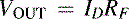
(14.6)
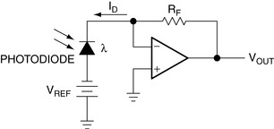 |
| Figure 14.8 Photodiode amplifier. |
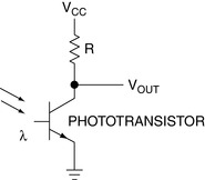
The phototransistor has a junction that is light sensitive, and the junction has a transparent cover so that it can sense ambient light. The collector base junction of the transistor is reverse biased, and normal transistor action takes place with the ambient light induced base current taking the place of the normal base current (see Figure 14.9).
 |
| Figure 14.9 Phototransistor amplifier. |
The photovoltaic or solar cell circuit is shown in Figure 14.10. The circuit zero biases the cell for minimum leakage current, and the cell's output current is a linear function of the area exposed to light. When the photovoltaic cell is properly masked and evenly flooded with light, it operates as a linear distance transducer, see Figure 14.10 and Equation (14.6).
 |
| Figure 14.10 Photovoltaic cell amplifier. |
AC excited transducers are usually used to make motion or distance sensors. In one type of AC excited transducer, a stationary winding is excited with an AC current and another winding is moved past the stationary winding, inducing a voltage in the second winding. In a well designed transducer, the induced voltage is proportional to distance, hence the output voltage is proportional to distance. Another AC excited transducer uses two plates: One plate is excited with an AC current, and the other plate is ground. An object coming near the excited plate changes the capacitance between the plates, and the result is an output voltage change.
Resolvers and synchros are position transducers that indicate position as a function of the phase angle between the exciting signal and the output signal. Resolvers and synchros normally are multiple winding devices excited from two or more sources. They indicate position very accurately, but their special circuitry requirements, cost, and weight limit them to a few applications such as airfoil control surfaces and gyros.
AC excited transducers require a rectifier circuit to make the output voltage unipolar prior to integration. Coarse transducers use a diode or diode bridge to rectify the output voltage, but diodes are not adequate for precision applications, because their forward voltage drop is temperature sensitive and poorly regulated. The diode problems are overcome through the use of feedback in the active full wave rectifier circuit shown in Figure 14.11. An integrating capacitor, C, is added to the circuit so the output voltage is a DC voltage proportional to the average voltage value of the input voltage.
 |
| Figure 14.11 Active full wave rectifier and filter. |
Semiconductor or wire junctions (thermocouples) are often used as temperature transducers because there is a linear relationship between temperature and output voltage over a restricted temperature range. Thermocouples have small voltages, varying from microvolt per degree Centigrade to millivolt per degree Centigrade, and they normally are configured with thermistors and zeroing resistors in the output circuit. Thermocouples have small output voltages and high output resistance, so a special op amp, called an instrumentation amplifier, is required for thermocouple amplification. An instrumentation amplifier has very high and equal input impedances, thus they don't load the input signal source.
Semiconductor junctions have a nominal temperature coefficient (TC) of −2 mV/°C. The TC is linear, but it varies from diode to diode because of manufacturing techniques, semiconductor materials, and bias currents. In a well controlled application, where thermal mass is insignificant, semiconductor junctions make excellent temperature transducers. The junction effect is so stable and linear that commercial temperature transducers have become available in a single IC.
Magnetic fields can be sensed by the Hall effect and special semiconductors called Hall effect sensors have been developed to sense magnetic fields. Current is passed through the semiconductor in a direction perpendicular to the magnetic field. A pair of voltage pick off leads is placed perpendicular to the direction of current flow, and the output voltage is proportional to the magnetic field strength. The manufacturing process for Hall effect transducers is a standard semiconductor manufacturing process, so Hall effect transducers are offered for sale as transistors or ICs.
14.3. Design Procedure
A step by step design procedure that results in the proper op amp selection and circuit design follows. This design procedure works best when the op amp has almost ideal performance, so the ideal op amp equations are applicable. When nonideal op amps are used, parameters like input current affect the design, and they must be accounted for in the design process. The latest generation of rail to rail op amps makes the ideal op amp assumption more valid than it ever was.
No design procedure can anticipate all possible situations; and depending on the op amp selected, procedure modifications may have to be made to account for op amp bias current, input offset voltage, or other parameters. This design procedure assumes that system requirements have determined the transducer and ADC selection and changing these selections adversely affects the project.
1 Review the system specifications to obtain specifications for noise, power, current drain, frequency response, accuracy, and other variables that might affect the design.
2 Characterize the reference voltage including initial tolerances and drift.
3 Characterize the transducer to determine its salient parameters, including output voltage swing, output impedance, DC offset voltage, output voltage drift, and power requirements. These parameters determine the op amp's required input voltage range (VIN1 to VIN2) and input impedance requirements. The offset voltage and voltage drift are tabulated as errors. At this point, it is assumed that the selected op amp's input voltage span is greater than the transducer's output voltage excursion. Design peripheral circuits if required.
4 Scrutinize the ADC's specification sheet to determine its required input voltage range, because this range eventually sets the op amp's output voltage swing requirement (VOUT1 to VOUT2). Determine the ADC's input resistance, input capacitance, resolution, accuracy, full scale range, and allowable input circuit charge time. Calculate the LSB value.
5 Create an error budget (in bits) for the transducer and ADC. Use the transducer/ADC error budget to determine the value and range of the critical op amp parameters. Select an op amp, and justify the selection by creating an error budget for the op amp circuit.
6 Scan the transducer and ADC specifications, and make a set of analog interface amplifier specifications
7 Complete the AIA circuit design.
8 Build the circuit, and test it.
14.4. Review of the System Specifications
The power supply has only one voltage available, and that voltage is 5 V ± 5% = 5 V ± 250 mV. The power supply is connected with the negative terminal at ground and the positive terminal at VCC. This is not a portable application, therefore the allowed current drain, 50 mA, is adequate for the job. No noise specifications are given, but the proposed power, ground, and signal traces are being done on high quality circuit board material with planes and good size copper. A system of this quality should experience no more than 50 mV of noise on the logic power lines and 10 mV of noise on the analog power lines.
This is a temperature measuring system that requires updates every 10 s. Clearly, ADC conversion speed or input charging rate is not cause for consideration. The low conversion speed translates into lower logic speed, and slow logic means less noise generated. The temperature transducer is located at the end of a 3 ft long cable, so expect some noise picked up by the cable to be introduced into the circuit. Fortunately, the long time between ADC conversions enable extensive filtering to reduce the cable noise.
The system accuracy required is 11 bits. The application measures several parameters, so it is multiplexed, and a TLV2544 12 bit resolution ADC has been selected. The temperature transducer is a diode, and the temperature span to be measured is −25°C to 100°C. The ambient temperature of the electronics package is held between 15°C to 35°C.
14.5. Reference Voltage Characterization
A reference voltage is required to bias the transducer and act as a reference voltage for the analog interface amplifier (AIA). Selecting a reference with a total accuracy better than the accuracy specification (11 bits) does not guarantee meeting the system accuracy specification, because other error sources exist in the design. Resistor tolerances, amplifier tolerances, and transducer tolerances all contribute to the inaccuracy, and the reference can't diminish these errors. The quandary here is a choice between an expensive reference and expensive accurate components or an adjustment to null out initial errors. This quandary boils down to which is the lesser of two evils: expensive components or the expense of an adjustment.
System engineering has decided that it wants the adjustment, so the reference need not have 11 bit accuracy. A TL431A voltage reference is chosen for the design. The output voltage specification at 25°C and 10 mA bias current is 2495 mV ± 25 mV. This reference has a temperature drift of 25 mV over 70°C, and this translates to 7.14 mV drift over a 20°C temperature range. Another drift is caused by the cathode voltage change, and this drift is 2.7 mV/V. The supply voltage regulation is 0.5 V, but much of this tolerance is consumed by the initial tolerance and wiring scheme, so the less than 0.1 V is due to regulator drift. The total drift is 7.14 mV + 0.27 mV = 7.41 mV. This yields a total drift of 0.3% maximum. The amplifier usually uses a fraction of the reference voltage, so the final AIA does not drift the full 0.3%.
14.6. Transducer Characterization
The temperature transducer is a special silicon diode characterized for temperature measurement work. When this diode is forward biased at 2.0 mA ± 0.1 mA, its forward voltage drop is 0.55 V ± 50 mV and its temperature coefficient is −2 mV/°C. The wide acceptable variation in bias current makes this an easy device to work with. The circuit for the bias calculations is shown in Figure 14.12.
 |
| Figure 14.12 Reference and transducer bias circuit. |
The current through RB1 is calculated in Equation (14.7). Remember, the reference must be biased at 10 mA and the transducer must be biased at 2 mA.
(14.7)
The value of RB1 is calculated in Equation (14.8) and the value of RB2 is calculated in Equation (14.9):
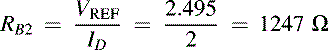
(14.8)
(14.9)
Both resistors are selected from the list of 1% decade values, therefore RB1 = 210 Ω, 1%, and RB2 = 1240 Ω, 1%. The resistor values have been established, so it is time to calculate the worst case excursions of ID, (14.10) and (14.11). The resistors are assumed to have a 2% tolerance in these calculations. The extra 1% allows for temperature changes, vibration, and life. Three percent tolerances would have been used if the electronics' ambient temperature range were larger.

(14.10)
(14.11)
The bias current extremes do not exceed the transducer bias current requirements, so the transducer meets the specifications advertised. The converter is 12 bits and the full scale voltage is assumed to be 5 V, so the value of an LSB is calculated in Equation (14.12). The nominal transducer output voltage is 550 mV at an ambient temperature of 25°C. At −25°C, the transducer output voltage is 550 mV + (−2 mV/°C)(−50°C) = 650 mV. At 125°C, the transducer output voltage is 550 mV + (−2 mV°C)(75°C) = 400 mV. These data are tabulated in Table 14.1.
(14.12)
| Transducer temperature | Transducer output voltage | Analog interface amplifier input voltage |
|---|---|---|
| −25°C | 650 mV | VIN1 = 650 mV |
| 25°C | 550 mV | 550 mV |
| 100°C | 400 mV | VIN2 = 400 mV |
The steady state (VTOS) offset voltage is ±50 mV, so transducer output voltage (VTOV) ranges from 350 mV to 700 mV. The offset voltage is stripped out by the adjustments in the AIA, so it is not of any concern here. VTOS spans 100 mV, so it is a 100 mV/1.22 mV/bit = 82 bit error unless it is adjusted out.
The output impedance of the transducer is equivalent to the resistance of a forward biased diode, Equation (14.13):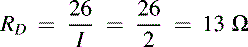
(14.13)
At this stage of the design, two parameters influence the accuracy of the measurement: the temperature coefficient of the transducer and the output impedance of the transducer. The temperature transducer has been biased correctly, so its temperature coefficient should be the advertised value of −2 mV/°C. The output impedance of the transducer forms a voltage divider with the input resistance of the AIA, but this error can't be calculated until the AIA is selected. The final transducer error contribution is that portion of the VTOS that can't be adjusted out, and this error is determined during the AIA design.
14.7. ADC Characterization
This particular ADC was selected because it has a multiplexer and it enables modes of operation. The temperature measurement is done in the single shot mode because this mode allows the user to set the charge time at the input to the converter. During charging, the ADC's input resistance is low, but after the ADC input is charged, the input resistance rises to 20 kΩ. This high input resistance does not load the AIA output circuit, so the AIA achieves full rail to rail output voltage swing.
The internal reference is used in this application, and the reference sets the input voltage span required to obtain full accuracy for the ADC. Using the internal reference, the input voltage span is 0 V to 4 V. The offset voltage (VADCOS) is ±150 mV, and the voltage drift is 40 PPM/°C. The voltage drift over the full temperature range is 40 PPM/°C(20°C) = 800 PPM. A 14 bit converter has 244 PPM/LSB, so the drift voltage error is 800/244 ≈ 4 bits error.
The ADC output is full scale (all bits 1) when the input voltage is 4 V, and it is zero (all bits 0) when the input voltage is 0 V. These data are tabulated in Table 14.2. Because the full scale output voltage has changed to 4 V, the LSB is calculated to be 4/(212) = 976.6 μV/bit.
14.8. Op Amp Selection
It is time to select the op amp, and the easiest way to do this is to list the known specifications or requirements, list a candidate op amp's specifications, and calculate the projected error that the candidate op amp yields (Table 14.3).
There should be almost no error from RIN, because the transducer output impedance is very low. The high side of the op amp's output voltage swing (4.85 V) is much higher than the ADC input voltage (4 V). The low side of the op amp's output voltage swing (0.185 V) is less than the ADC input voltage swing (0 V). The ADC input circuit is 20 kΩ, and that doesn't load the op amp output stage, so the op amp output voltage swing is very close to the ADC input voltage range. ROUT should present no problems acting as a voltage divider with the ADC input resistance. VOS and IIB create offset voltages that add to the reference offset voltage, and they have to be adjusted out as a group. The system noise overshadows the op amp noise, so the op amp noise is accepted unless later calculations prove otherwise.
14.9. Amplifier Circuit Design
Enough information exists for the AIA to be designed. The TLV247X op amp is selected because it meets all the system requirements. The first step in the design is to determine the AIA input and output voltages, and this has already been done. These voltages are taken from Table 14.1 and Table 14.2 and repeated here as Table 14.4.
| Input voltage | Output voltages | |
|---|---|---|
| VIN1 = 650 mV | VOUT1 = 0 V | First pair of data points |
| VIN2 = 400 mV | VOUT2 = 4 V | Second pair of data points |
The equation of an op amp is the equation of a straight line, as given in Equation (14.14):
(14.14)
The two pairs of data points shown in Table 14.4 are substituted in Equation (14.14), making (14.15) and (14.16):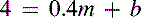

(14.15)
(14.16)
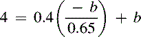
Solving Equation (14.17) yields b = 10.4, and solving Equation (14.15) yields m = −16. Substituting these values back into Equation (14.14) yields Equation (14.18) and Equation (14.18) (the final equation for the AIA) is put in electronic terminology:
(14.18)
The circuit that yields the transfer function developed in Equation (14.18) is shown in Figure 14.13.
 |
| Figure 14.13 AIA circuit. |
The equations for the AIA circuit follow: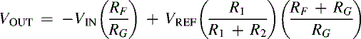

(14.19)
(14.20)
(14.21)
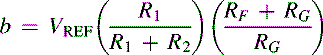
Equation (14.18) gives the value for m as 16, and using Equation (14.20) yields RF = 16RG. Select RF = 383 kΩ and RG = 23.7 kΩ, because they are standard 1% resistor values, and this yields m = 16.16. The resistors R1 and R2 are calculated with the aid of (14.22) and (14.23):

(14.22)
(14.23)
The parallel combination of R1 and R2 should equal the parallel combination of RF and RG, so that the input voltage offset caused by the op amp input current is canceled. Select R2 = 105 kΩ and R1 = 33.2 kΩ, because they are standard 1% values, then b = 10.3. The value of the parallel combination of R1, R2 (R1∥R2 = 25.22 kΩ) almost matches the value of the parallel combination of RF, RG (RF∥RG = 22.3 kΩ), and this is an adequate match for input current cancelation. The downsides of selecting large resistor values for RF are current noise amplification, increased resistor noise, smaller bandwidth because of stray capacitance, and increased offset voltage due to input current. Bandwidth clearly is not a factor in this design. The op amp input current is 100 pA, so it won't cause much offset with a 383 kΩ feedback resistor (38.3 μV). The noise current and voltage are calculated later when the error budget is made.
The gain, m, and the intercept, b, are not accurate, because the exact resistor values were not available in the 1% resistor selection chart. This is a normal situation; and in less demanding designs, the small error either does not matter or is corrected someplace else in the signal chain. That error is critical in this design, so it must eliminated. Several nondrift type errors have accumulated up to this point, and now is the time to correct all the nondrift errors with the addition of adjustments. Two adjustments are used: one adjustment controls the gain, m, and the other controls the intercept, b. The value of the adjustable resistor must be large enough to deliver an adequate adjustment range, but any value larger than that decreases the adjustment resolution.
The data that determine the adjustment range required are tabulated in Table 14.5. Drift and gain errors are calculated in volts, but drift errors are calculated in bits because they are not eliminated by adjustments. Remember, an LSB for this system is 4/4096 = 976.6 μV/bit.
The adjustment for the intercept, b, depends on R1, R2, and VREF. This adjustment has to account for the reference offset, the op amp input voltage offset, the op amp input current, and the resistor tolerances. The offset voltage inherent in the reference is given as ±25 mV. The op amp input offset voltage is 2.2 mV; usually op amp offset voltage calculations include multiplying this offset by the closed loop gain, but this isn't done because the offset voltage is adjusted out in the input circuit. The op amp input current is converted to a common mode voltage by the parallel combination of the reference resistors, so it is neglected in this calculation.
The worst case reference input voltage for the op amp, VREF(MIN), is calculated in Equation (14.24), where the resistor tolerances are assumed to be 3% and the reference voltage error is 50 mV:
(14.24)
The nominal reference voltage at the op amp input is 0.6 V, so the reference voltage has to have about 40 mV adjustment around the nominal, or a total adjustment range of 80 mV. The nominal current through the voltage divider is IDIVIDER = [2.495/(105 + 33.2)] kΩ = 0.018 mA. A 4444 kΩ resistor drops 80 mV, so the adjustable resistor (a potentiometer) must be greater than 4444 kΩ. Select the adjustable resistor, R1A, equal to 5 kΩ because this is an available potentiometer value, and the offset adjustment is ±45 mV. Half of the potentiometer value is subtracted from R1 to yield R1B, and this subtraction centers the adjustment about the nominal value of 0.6 V. R1B = 33.2 kΩ − 2.5 kΩ = 30.7 kΩ. Select R1B as 30.9 kΩ.
The adjustment for the gain employs RF and RG to ensure that the gain can always be set at the value required to ensure that the transducer output swing fills the ADC input range. The gain equation, Equation (14.18), is algebraically manipulated, worst case values are substituted for m and b, and it is presented as Equation (14.25):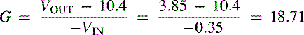
(14.25)
Doing the arithmetic in Equation (14.26) yields RF = 19.86RG. Therefore, on the high side, the gain must go from 16 to 19.86, or it must increase by 3.86. Assuming that the low side gain variation is equal and rounding off to 4 sets the gain variation from 12 to 20. When RG = 23.7 kΩ, RF varies from 284.4 kΩ to 474 kΩ. RF is divided into a potentiometer RFA = 200 kΩ and RFB = 280 kΩ, thus the nominal gain can be varied from 11.8 to 20.2 (see Figure 14.14).
There is no easy method of setting two interacting adjustments, because when the gain is changed, the offset voltage changes. They quickest method of adjustment is to connect the transducer to the circuit, adjust the offset, then adjust the gain. It takes several series of adjustments to get to the point where the both parameters are set correctly.
The impedance and noise errors are calculated prior to completing the error budget. The op amp input impedance works against the transducer output impedance to act like a voltage divider. The value of the voltage divider is calculated in Equation (14.27); and as Equation (14.27) indicates, the output resistance of the transducer is negligible compared to the input resistance of the op amp. This is not always the case!
(14.27)
The ADC input impedance works against the op amp output impedance to act like a voltage divider. The value of the voltage divider is calculated in Equation (14.28). The voltage divider action introduces about a 0.009% error into the system, and this is within 13 bit accuracy, so it can be neglected.
(14.28)
The noise specification is given in nV/(Hz0.5), and this must be converted to volts. Involved formulas are used for the conversion, but the simplest thing to do is assume the noise is wideband. If the numbers add up to a significant error, detailed calculations have to be made. The voltage noise is multiplied by the closed loop gain, therefore VNWB = VN(GMAX) = 28 nV(20) = 560 nV = 0.56 μV. The current noise is multiplied by the parallel combination of RF and RG, so INWBIN(RF∥RG) = 139 pA(22.5 kΩ) = 3.137 nV. The system noise is 10 mV, and this noise comes in through the inputs and the power supply. The power supply contribution is reduced by the power supply rejection ratio, and it is 10 mV/63 dB = 10 mV/1412 = 7.08 nV. This calculation assumes that high frequency noise is not a problem; but if this is not true, CMRR must be reduced per the data sheet CMRR versus frequency curves.
Some of the system noise propagates through the inputs and is rejected by the common mode rejection of the op amp. The op amp is not configured as a differential amplifier, so a portion of the closed loop gain multiplies some of the system noise.
The AC gain of the AIA is given in Equation (14.29):
(14.29)
All of the system noise does not get in on the inputs, rather most of the system noise is found on the power supply. The fraction of the system noise that gets into the ground system and onto the op amp inputs is very small. This fraction, α, is normally about 0.01 because the power supplies are heavily decoupled to localize the noise. Considering this, the system noise is 1.18 mV, or less than 2 LSBs.
The op amp output voltage range does not include 0 V, and the ADC output voltage low value is 0 V, so this introduces another error. The guaranteed op amp low voltage is 185 mV at a load current of 2.5 mA. The output current in this design is 185 mV/20 kΩ = 9.25 μA. This output current approximates a no load condition, hence the nominal low voltage typical specification of 70 mV is used. This leads to a 72 LSB error, by far the biggest error.
Referring to Table 14.5, note that the total error is 90 LSB. Losing 90 LSBs out of 4096 total LSBs is approximately 11.97 bits accurate, so the 11 bit specification is met. The final circuit is shown in Figure 14.14.
 |
| Figure 14.14 Final analog interface circuit. |
Note that large decoupling capacitors have been added to the power supply and reference voltage. The decoupling capacitors localize IC noise, prevent interaction between circuits, and help keep noise from propagating. Two decoupling capacitors are used, a large electrolytic for medium and low frequencies and a ceramic for high frequencies. Although this portion of the design is low frequency, the op amp has a good frequency response, and the decoupling capacitors prevent local oscillations through the power lines. If cable noise is a problem, an integrating capacitor can be put in parallel with RF to form a low pass filter.
14.10. Test
The final circuit is ready to build and test. The testing must include every possible combination of transducer input and ADC output to determine that the AIA functions in all manufacturing situations. The span of the adjustments, op amp output voltage range, and ADC input range must be checked for conformance to the design criteria. After the design has been tested for the specification limits, it should be tested for user abuse. What happens when the power supply is ramped up, turned on instantly, or something between these two limits? What happens when the inputs are subjected to overvoltage or the polarity is reversed? These are a few ideas to guide your testing.
14.11. Summary
The systems engineers select the transducer and ADC, and their selection criterion is foreordained by the application requirements. The AIA design engineer must accept the selected transducer and ADC, and it is the AIA designer's job to make these parts play together with adequate accuracy. The AIA design often includes the design of peripheral circuits, like transducer excitation circuits, and references.
The design procedure starts with an analysis of the transducer and ADC. The analysis is followed by a characterization of the transducer and reference. At this point, enough information is available to make an error budget and select candidate op amps. The op amp is selected in the next step in the procedure, and the circuit design follows.
The output voltage span of the transducer and corresponding input voltage span of the ADC are coupled as two pairs of data points that form the equation of a straight line. The data point pairs are substituted into simultaneous equations, and the equations are solved to determine the slope and intercept of a straight line (an op amp solution). The op amp circuit configuration is selected based on the sign of the slope and the intercept. Finally, the passive components used in the op amp circuit are calculated with the aid of the op amp circuit design equations.
The final circuit must be tested for conformance to the system specifications, but the prudent engineer tests beyond these specifications to determine the AIA's true limits.
Reference
1. Darold Wobschall, Circuit Design for Electronic Instrumentation. (1979) McGraw-Hill, New York.
..................Content has been hidden....................
You can't read the all page of ebook, please click here login for view all page.