
Chapter 15. Interfacing an Op Amp to an Analog to Digital Converter
15.1. Introduction
One of the most common questions asked by customers is, “Which op amp should I use with a given data converter?” The answer is enough to make a marketing engineer cringe, because it depends on the answers to many questions—way too many to be in the customer's comfort zone. Yet, the answers to these questions are not only necessary for the customer's design to be a success, they are questions that a customer must eventually answer.
It would be handy to have a table with A/D converters on one side and recommended op amps on the other. But this table will never exist—too many variables in system design affect the choice of op amp. The questions in this chapter help organize the designer's thoughts into the correct direction and define the issues. These questions are the ones that a designer should be prepared to answer, before committing to a design.
The list of questions may look daunting at the beginning, but they are divided into sections. This breaks up the system into component parts that surround the op amp and define exactly what that component needs to do. The completion of each section is a piece of the puzzle, and by the end of the process, the designer should have weeded out op amps that are unsuitable for the job.
Once the op amp has been selected, the job is not done. Some architectural considerations for the signal chain and trade-offs are associated with each one. A few of the most useful options are explored.
15.2. System Information
The overall characteristics of the system oftentimes yield valuable information. A clear understanding of the product and its function is imperative to design success:
• Exactly what is the end equipment and its application? Different systems have different requirements. For example, key concerns in a video system are completely different than those in a wireless communication system.
• In general terms, what is the function of this signal acquisition chain in the system? Where does the input signal come from and what happens to it once it is digitized?
• How many signal acquisition chains are used in the product? Channel density can influence system design in numerous ways, including space constraints, thermal requirements, and amplifier channel density per package.
• Will this signal chain be duplicated in other products? Is flexibility an advantage or can the design be narrowly focused on the task at hand?
• Is the design forced to adhere to a particular standard?
• Under what temperature conditions will the system operate; for example, −40°C to +85°C, 0°C to +70°C, +45°C to +55°C?
• Does the system have forced airflow from a fan to help with thermal dissipation?
• Is automatic gain control (AGC) functionality required? If so, is it digital or analog control? What is the gain range and so forth?
• Is a current solution unsatisfactory in some way? Why is the current solution unsatisfactory?
15.3. Power Supply Information
Power supply rails can quickly rule out amplifier solutions (Figure 15.1). This is similar to clothing shopping—the style may be desirable, but if the size doesn't fit, the style is useless. So a wise shopper finds the options in the size first, before becoming attached to a style. Similarly, an op amp with fantastic specifications at ±15 V may not operate at all from a +3.3 V power supply. Power supply information is collected first, because it simply and unequivocally narrows the choices:
• What is the power budget for the overall system? Is power a concern or is performance the ultimate goal?
• What power supply voltages are available in the design?
• Is there a preferred power supply voltage for the amplifier circuitry?
• Can an additional supply voltage be added if performance could be improved? Often, the best amplifier performance can be obtained with split supplies.
• Is a precision reference available in the system? In single supply systems, it is important to supply a virtual ground to the op amp circuitry. If the system already contains a reference, it may be possible to utilize it.
• Are there any special characteristics of the power supply? For example, is the power supply a switching power supply? Although op amps usually have excellent power supply rejection, it could be a concern in high resolution system. Any widely varying loads could also affect the op amp supply voltage.
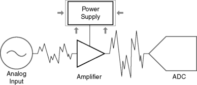 |
| Figure 15.1 Focusing on the power supply characteristics. |
15.4. Input Signal Characteristics
Understanding the input source (Figure 15.2) is key to properly designing the interface circuitry between the source and the analog to digital converter:
• What is used for the signal source to the amplifier block in front of the ADC? Is it another amplifier, a sensor, or what?
• Describe the input signal. For example, is it continuous or discontinuous (i.e., pulsed)? The signal might be a QAM signal, an NTSC signal, a nonstandard continuous wave signal, a random analog signal, or some other signal.
• Are there any unusual characteristics of the signal source? Some sources have characteristics that affect the performance of the amplifier circuit. For example, photodiodes have an associated capacitance, and the value of this capacitance plays an important role in designing the associated amplifier circuit.
• What is the output amplitude range of the source?
• Does the source produce a voltage or a current output?
• Is the signal source output single ended or differential?
• What is the output impedance of the signal source?
• Is the input signal DC referenced? If so, to what DC voltage is it referenced?
• What are the frequency characteristics of the input signal? For example, the signal might have a 10 MHz bandwidth centered around 25 MHz or it might be a signal with frequency content from DC up to 20 MHz. If low frequency isn't important, this opens the possibility of AC coupling the input signal.
• What level of rejection is required out of band? Some applications have very strict requirements for out of band rejection, while others are less strict. The filter interface between the amplifier network and the ADC is dictated by this sort of information.
• Must a known interfering frequency (such as a system clock or sample clock) be filtered out? Are other large signals expected outside of the band of interest? Oftentimes, a simple low pass filter may not have sufficient rejection of a particular interfering signal, forcing additional circuitry to produce a high Q notch filter.
• Is there a requirement for gain or phase flatness or error? This is a concern in video systems.
• Is there a matching requirement on the input impedance of the amplifier circuit? Some circuits require that the load seen is matched to a particular value for optimum performance (e.g., 50 Ω).
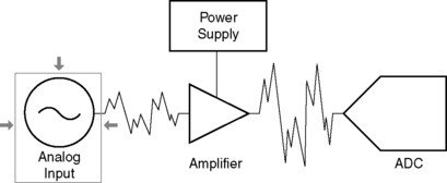 |
| Figure 15.2 Focusing on the input signal. |
15.5. Analog to Digital Converter Characteristics
Now that the power supply and input signal have been defined, it is time to focus on the device that the op amp will drive, the analog to digital converter (Figure 15.3):
• Has the analog to digital converter been selected or is it possible to change the converter if performance can be enhanced?
• What is the desired sampling rate? Often, people assume that a data converter is going to be used at its maximum level of performance, but this typically isn't the case. For example, an 80 MSps (megasample per second) converter might be given a sampling frequency of 60 MSps.
• What is the desired resolution and effective number of bits? A 14 bit converter won't effectively yield 14 bits. The true resolution probably is closer to 12 or 13.
• What is the full scale input range of the data converter? Some data converters have the option of configuring the input for different ranges.
• Will the data converter be used with single ended or differential inputs? Typically, most high performance data converters have differential inputs and require their use for optimum performance.
• Could any other options on the data converter be an advantage? Data converters have lots of options that vary from part to part. The most important feature of some ADCs is the availability of a precision reference that can be used for the op amp interface circuitry.
• Are there any compensation requirements for the input of the data converter? Normally, a small RC filter is required at the input of the data converter to compensate for its capacitive input. These components are usually specified in the converter data sheet and should be included as part of the interface. Otherwise, the op amp interface circuit may exhibit instability.
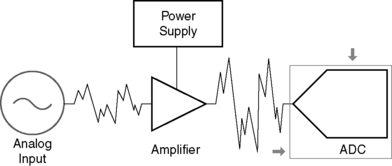 |
| Figure 15.3 Focusing on the analog to digital converter. |
15.6. Operational Amplifier Characteristics
Although this chapter is intended to aid in the selection of the correct operational amplifier (Figure 15.4), it is possible that the nature of the system already defines some op amp characteristics:
• Has the selection of operational amplifier already been made or can it be changed if performance of the system could be improved?
• Are there specific requirements for the package of the amplifiers? For example, must it be an 8 pin SOIC or as small as possible?
• Does the cost of the operational amplifier interface or the physical size of the interface circuitry dictate that as few operational amplifiers as possible be used or would it be an advantage for the circuitry to be easily modified in the future, using more operational amplifiers for the flexibility?
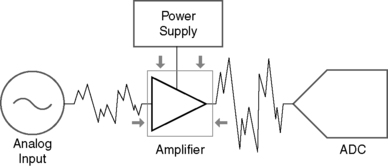 |
| Figure 15.4 Focusing on the operational amplifier. |
15.7. Architectural Decisions
The job is still not done. A decision must be made at this point: How will the signal chain (and interface) be implemented. The guidelines in this chapter are not meant to be device specific for every data converter or op amp, rather they are general cases that can be used as a basis for design. Let's get started.
In some cases, such as IF baseband, the best interface may well be no op amp at all but a simple transformer over a narrow frequency band, which has been employed successfully in many designs. As the title of this publication is Op Amps for Everyone, purely transformer interfaces are not explored at length, however a transformer may be employed in combination with op amps when gain is required.
Besides the transformer, the other decisions are
• To use single ended or fully differential op amps.
• Whether to power the interface from a single supply or split supplies (if possible).
• Whether to reference the input to ground (single ended) or make it fully differential.
• Whether the interface circuit can be AC coupled or must the operational range include DC.
• Whether the data converter can or should be referenced to ground or should it be operated in fully differential mode.
Some of the decisions may be premade, such as the selection of data converter or the power supplies (split versus single supply).
Figure 15.5 shows one of the simplest interface circuits. The CM pin of the data converter is used to set the common mode input of the fully differential op amp. The data converter compensation inputs are shown (R5/C1 and R6/C2). An input termination resistor, usually 50 Ω, is shown but may or may not be utilized. Gain of the op amp interface is set by R1 through R4, the common mode input range of the data converter includes ground, and the frequency response extends from DC to the bandwidth limit of the op amp circuit.
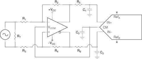 |
| Figure 15.5 Fully differential DC coupled interface. |
While this circuit is very nice, it is also not very typical of real world applications. To begin with, the op amp interface operates from split supplies, which may not be available in the system. Also, most input signals are referenced to ground, which presents its own set of challenges.
Figure 15.6 shows a more typical interface circuit. The input signal is referenced to ground, while the common mode operating point of the op amp interface is set by the data converter. The op amp interface can be run off of a single supply.
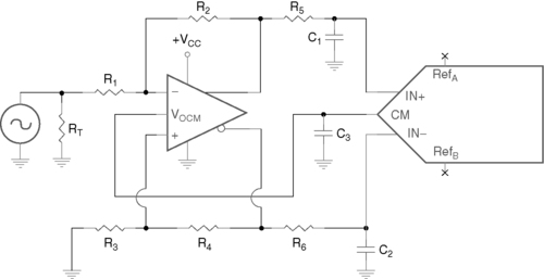 |
| Figure 15.6 Single ended to fully differential DC coupled interface. |
This configuration is covered in more detail in a later chapter, one devoted to application errors. Suffice it to say, a circuit such as this must be applied carefully.
There are several keys to the successful application of this circuit:
• The first is to be aware of the DC gain and DC operating point of the circuit. This will probably limit the AC gain severely.
• It is important to utilize an op amp that includes ground in its common mode range. Texas Instruments manufactures an op amp specifically for this configuration, the THS4500.
• If the input has to be terminated, as shown in Figure 15.6, the value of the termination resistor affects the values of the other resistors. This is covered in Section 11.6.
It is not absolutely necessary to utilize a fully differential op amp to drive a differential data converter. Figure 15.7 shows the preferred method to drive a fully differential op amp using single ended op amps. The input signal is referenced to ground, and decoupling from the op amp interface is accomplished by using a transformer. Each phase of the output signal is handled in a conventional inverting op amp stage, and the common mode point for both amplifiers is set by the data converter. Remember that, if termination is employed, it must be reflected through the transformer. For a 1:1 transformer, RT1 equals RT2.
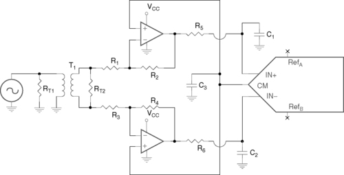 |
| Figure 15.7 Single ended to fully differential AC coupled interface. |
Figure 15.8 shows the preferred way to convert single ended signals to differential without a transformer. While this circuit looks a bit unusual, the strategy is to equalize the delay for IN+ and IN– by forcing each phase of the signal to go through both op amps before being applied to the inputs. This may not be intuitive at first glance! Each amplifier, though, is in the feedback loop for the other. Think of this as an inverting op amp circuit—gain is adjusted by changing R1 (corresponding to RG), R2 through R6 are equal values (corresponding to RF). If DC gains are taken into account, this circuit also works for DC coupled applications.
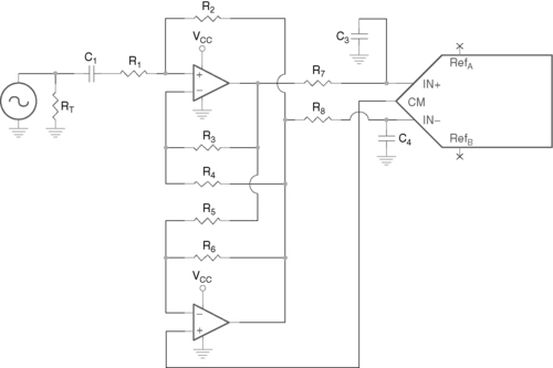 |
| Figure 15.8 Preferred single ended to fully differential AC coupled interface. |
..................Content has been hidden....................
You can't read the all page of ebook, please click here login for view all page.